


AUSTN AS8S512K32Q-55L-XT, AS8S512K32Q-55L-IT, AS8S512K32Q-55L-883C, AS8S512K32Q-45L-XT, AS8S512K32Q-45L-883C Datasheet
...
|
|
SRAM |
|
|
|
AS8S512K32 |
|
|
Austin Semiconductor, Inc. |
& AS8S512K32A |
|
512K x 32 SRAM |
|
|
|
PIN ASSIGNMENT |
|
|||||||||
SRAM MEMORY ARRAY |
|
|
|
(Top View) |
|
|
|
|
||||||
AVAILABLE AS MILITARY |
|
|
|
68 Lead CQFP (Q) |
|
|
|
|||||||
SPECIFICATIONS |
|
|
|
|
Military SMD Pinout Option |
|
||||||||
• SMD 5962-94611 (Military Pinout) |
|
|
NC A0 A1 A2 A3 A4 A5 CS3\ |
GND CS4\ |
WE1\ |
A6 A7 A8 |
A9 |
A10 |
Vcc |
|
||||
|
|
|
|
|
|
|
|
|
|
|
||||
• |
MIL-STD-883 |
|
|
|
|
9 8 7 6 5 4 3 2 1 8 7 6 5 4 3 2 1 |
|
|||||||
FEATURES |
|
|
|
I/O 0 |
1 0 |
|
6 6 6 6 6 6 6 6 |
I/O 16 |
||||||
|
|
|
|
|
|
|
|
|
6 0 |
|||||
|
|
|
I/O 1 |
1 1 |
|
|
|
|
|
|
5 9 |
I/O 17 |
||
• Operation with single 5V supply |
|
|
I/O 2 |
1 2 |
|
|
|
|
|
|
5 8 |
I/O 18 |
||
|
|
I/O 3 |
1 3 |
|
|
|
|
|
|
5 7 |
I/O 19 |
|||
• High speed: 17, 20, 25 and 35ns |
|
|
I/O 4 |
1 4 |
|
|
|
|
|
|
5 6 |
I/O 20 |
||
|
|
I/O 5 |
1 5 |
|
|
|
|
|
|
5 5 |
I/O 21 |
|||
• Built in decoupling caps for low noise |
|
|
|
|
|
|
|
|||||||
|
I/O 6 |
1 6 |
|
|
|
|
|
|
5 4 |
I/O 22 |
||||
|
|
|
|
|
|
|
|
|
|
|
|
|
|
|
• Organized as 512Kx32 , byte selectable |
|
I/O 7 |
1 7 |
|
|
|
|
|
|
5 3 |
I/O 23 |
|||
|
GND |
1 8 |
|
|
|
|
|
|
5 2 |
GND |
||||
• |
Low power CMOS |
|
|
|
I/O 8 |
1 9 |
|
|
|
|
|
|
5 1 |
I/O 24 |
|
|
|
I/O 9 |
2 0 |
|
|
|
|
|
|
5 0 |
I/O 25 |
||
• TTL Compatible Inputs and Outputs |
|
I/O 10 |
2 1 |
|
|
|
|
|
|
4 9 |
I/O 26 |
|||
|
2 2 |
|
|
|
|
|
|
|||||||
• |
Future offerings |
|
|
|
I/O 11 |
|
|
|
|
|
|
4 8 |
I/O 27 |
|
|
|
|
I/O 12 |
2 3 |
|
|
|
|
|
|
4 7 |
I/O 28 |
||
|
3.3V Power Supply |
|
|
|
I/O 13 |
2 4 |
|
|
|
|
|
|
4 6 |
I/O 29 |
|
|
|
|
I/O 14 |
2 5 |
|
|
|
|
|
|
4 5 |
I/O 30 |
|
|
15 ns Ultra High Speed |
|
|
|
I/O 15 |
2 6 |
2 8 2 9 3 0 3 1 3 2 3 3 3 4 |
3 5 3 6 |
3 7 |
3 8 3 9 4 0 |
4 1 |
4 2 |
4 4 |
I/O 31 |
|
|
|
|
2 7 |
4 3 |
|||||||||
OPTIONS |
MARKINGS |
|
Vcc A11 A12 A13 A14 A15 A16 CS1\ |
OE\ CS2\ |
A17 |
WE2\ WE3\ WE4\ |
A18 |
NC |
NC |
|
||||
|
|
68 Lead CQFP |
|
|
|
|
||||||||
• |
Operating Temperature Ranges |
|
|
|
|
|
|
|
|
|||||
|
|
Commercial Pinout Option (A) |
|
|||||||||||
|
Military (-55oC to +125oC) |
XT |
|
|
||||||||||
|
Industrial (-40oC to +85oC) |
IT |
|
|
I/O 16 |
A18 A17 CS4\ CS3\ CS2\ CS1\ NC |
Vcc NC |
NC |
OE\ WE\ A16 |
A15 |
A14 |
I/O 15 |
|
|
|
|
|
|
|
|
|
||||||||
• |
Timing |
|
|
|
I/O17 |
9 8 7 6 5 4 3 2 1 8 7 6 5 4 3 2 1 |
I/O 14 |
|||||||
|
|
|
1 0 |
|
|
|
|
|
|
6 0 |
||||
|
|
|
|
|
|
|
|
6 6 6 6 6 6 6 6 |
|
|||||
|
17ns |
|
-17 |
|
I/O18 |
1 1 |
|
|
|
|
|
|
5 9 |
I/O 13 |
|
|
|
I/O19 |
1 2 |
|
|
|
|
|
|
5 8 |
I/O 12 |
||
|
20ns |
|
-20 |
|
Vss |
1 3 |
|
|
|
|
|
|
5 7 |
Vss |
|
25ns |
|
-25 |
|
I/O20 |
1 4 |
|
|
|
|
|
|
5 6 |
I/O 11 |
|
|
|
I/O21 |
1 5 |
|
|
|
|
|
|
5 5 |
I/O 10 |
||
|
35ns |
|
-35 |
|
I/O22 |
1 6 |
|
|
|
|
|
|
5 4 |
I/O 9 |
|
|
|
I/O23 |
1 7 |
|
|
|
|
|
|
5 3 |
I/O 8 |
||
|
45ns |
|
-45 |
|
Vcc |
1 8 |
|
|
|
|
|
|
5 2 |
Vcc |
|
|
|
I/O24 |
1 9 |
|
|
|
|
|
|
5 1 |
I/O 7 |
||
|
55ns |
|
-55 |
|
|
|
|
|
|
|
||||
|
|
|
I/O25 |
2 0 |
|
|
|
|
|
|
5 0 |
I/O 6 |
||
|
|
|
|
|
I/O26 |
2 1 |
|
|
|
|
|
|
4 9 |
I/O 5 |
|
|
|
|
|
I/O27 |
2 2 |
|
|
|
|
|
|
4 8 |
I/O 4 |
• |
Package |
|
|
|
Vss |
2 3 |
|
|
|
|
|
|
4 7 |
Vss |
|
Q |
No.702 |
I/O28 |
2 4 |
|
|
|
|
|
|
4 6 |
I/O 3 |
||
|
Ceramic Quad Flatpack |
|
I/O29 |
2 5 |
|
|
|
|
|
|
4 5 |
I/O 2 |
||
|
|
|
|
|
I/O30 |
2 6 |
|
|
|
|
|
|
4 4 |
I/O 1 |
|
Pin Grid Array |
|
P |
No.904 |
7 8 9 0 1 2 3 4 5 6 7 8 9 0 1 2 3 |
|||||||||
|
|
|
2 2 2 3 3 3 3 3 3 3 3 3 3 4 4 4 4 |
|
||||||||||
• Low Power Data Retention Mode |
L |
|
|
I/O 31 |
A6 A5 A4 A3 A2 A1 A0 |
Vcc A13 A12 A11 A10 A9 A8 A7 |
I/O 0 |
|
||||||
• |
Pinout |
|
|
|
|
|
66 Lead PGA (P) |
|
|
|
||||
|
|
|
|
|
Military SMD Pinout |
|
|
|||||||
|
Military |
|
(no indicator) |
|
|
|
|
|
|
|
|
|
|
|
|
Commercial |
|
A |
|
|
|
|
|
|
|
|
|
|
|
GENERAL DESCRIPTION |
|
|
CS |
|
|
|
|
|
|
CS |
|
|||
|
|
|
|
|
|
|
|
|
|
|
||||
|
The Austin Semiconductor, Inc. AS8S512K32 and |
|
|
|
|
|
|
|
|
|
|
|||
AS8S512K32A are 16 Megabit CMOS SRAM Modules organized as |
|
|
|
|
|
|
|
|
|
|
||||
512Kx32 bits. These devices achieve high speed access, low power |
|
|
\ |
|
|
|
|
|
|
|
||||
|
|
|
|
|
|
|
|
|
|
|||||
consumption and high reliability by employing advanced CMOS |
|
|
|
|
|
|
|
|
|
|
||||
memory technology. |
|
|
|
|
|
|
|
|
|
|
|
|
|
|
|
This military temperature grade product is ideally suited for |
|
|
|
|
|
|
|
|
|
|
|||
military and space applications. |
|
|
|
|
CS |
|
|
|
|
|
|
CS |
|
|
|
For more products and information |
|
|
|
|
|
|
|
|
|
|
|||
|
please visit our web site at |
|
|
|
|
|
|
|
|
|
|
|
||
|
www.austinsemiconductor.com |
|
|
|
|
|
|
|
|
|
|
|||
|
|
|
AS8S512K32 & AS8S512K32A |
Austin Semiconductor, Inc. reserves the right to change products or specifications without notice. |
|
Rev. 3.1 12/01 |
1 |
|
|
|
|
|
|
SRAM |
|
|
|
AS8S512K32 |
|
|
Austin Semiconductor, Inc. |
& AS8S512K32A |
|
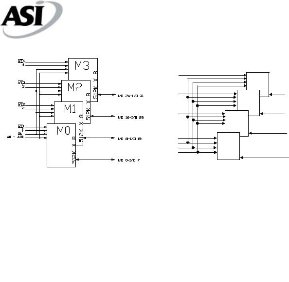
CS
CS
CS
CS
CS4\CS\4
CS3\CS\3
CS2\CS\2
CS1\CS\1
WE\
OE\ A0 - A18
|
|
M3 x8 |
||
|
|
M2 |
8 |
512K |
|
|
|
512K x |
|
M1 |
8 |
|
|
|
|
|
512K x |
|
|
M0 |
8 |
|
|
|
|
512K x |
|
|
|
 I/O 24 - I/O 31
 I/O 16 - I/O 23
 I/O 8 - I/O 15
 I/O 0 - I/O 7
MILITARY PINOUT/BLOCK DIAGRAM |
COMMERCIAL PINOUT/BLOCK DIAGRAM |
TRUTH TABLE
MODE |
OE\ |
CSE\ |
WE\ |
I/O |
POWER |
Read |
L |
L |
H |
DOUT |
ACTIVE |
Write(2) |
X |
L |
L |
DIN |
ACTIVE |
Standby |
X |
H |
X |
High Z |
STANDBY |
|
|
|
AS8S512K32 & AS8S512K32A |
Austin Semiconductor, Inc. reserves the right to change products or specifications without notice. |
|
Rev. 3.1 12/01 |
2 |
|
|
|
|

|
|
SRAM |
|
|
|
AS8S512K32 |
|
|
Austin Semiconductor, Inc. |
& AS8S512K32A |
|
ABSOLUTE MAXIMUM RATINGS*
Voltage of Vcc Supply Relative to Vss...................... |
-.5V to +7V |
Storage Temperature............................................ |
-65°C to +150°C |
Short Circuit Output Current(per I/O)................................. |
20mA |
Voltage on Any Pin Relative to Vss.................... |
-.5V to Vcc+1V |
Maximum Junction Temperature**................................... |
+150°C |
*Stresses greater than those listed under “Absolute Maximum Ratings” may cause permanent damage to the device.
This is a stress rating only and functional operation on the device at these or any other conditions above those indicated in the operational sections of this specification is not implied. Exposure to absolute maximum rating conditions for extended periods may affect reliability.
**Junction temperature depends upon package type, cycle time, loading, ambient temperature and airflow. See the Application Information section at the end of this datasheet for more information.
ELECTRICAL CHARACTERISTICS AND RECOMMENDED DC OPERATING CONDITIONS
(-55oC < TA < 125oC and -40oC to +85oC; Vcc = 5V +10%)
DESCRIPTION |
CONDITIONS |
SYMBOL |
|
MIN |
|
MAX |
UNITS |
|
NOTES |
|||||||||||
Input High (logic 1) Voltage |
|
|
|
|
VIH |
|
2.2 |
|
|
VCC+.5 |
V |
|
1 |
|||||||
Input Low (logic 1) Voltage |
|
|
|
|
VIL |
|
-0.5 |
|
|
|
0.8 |
V |
|
1,2 |
||||||
Input Leakage Current ADD,OE |
0V<VIN<VCC |
|
ILI1 |
|
-10 |
|
|
|
10 |
μA |
|
|
|
|||||||
Input Leakage Current WE, CE |
|
ILI2 |
|
-10 |
|
|
|
10 |
μA |
|
|
|
||||||||
|
|
|
|
|
|
|
|
|
|
|
||||||||||
Output Leakage Current I/O |
Output(s) Disabled |
ILO |
|
-10 |
|
|
|
10 |
μA |
|
|
|
||||||||
0V<VOUT<VCC |
|
|
|
|
|
|
|
|||||||||||||
|
|
|
|
|
|
|
|
|
|
|
|
|
|
|
|
|
|
|||
Output High Voltage |
|
IOH = 4.0mA |
|
VOH |
|
2.4 |
|
|
|
|
|
V |
|
1 |
||||||
Output Low Voltage |
|
IOL = 8.0mA |
|
VOL |
|
|
|
|
|
0.4 |
V |
|
1 |
|||||||
Supply Voltage |
|
|
|
|
|
|
VCC |
|
4.5 |
|
|
|
5.5 |
V |
|
1 |
||||
|
|
|
|
|
|
|
|
|
|
|
|
|
|
|
|
|
|
|
|
|
|
|
|
|
|
|
|
|
|
|
MAX |
|
|
|
|
|
|
|
|
|
|
DESCRIPTION |
|
CONDITIONS |
SYMBOL |
|
-17 |
|
-20 |
|
-25 |
|
-35 |
|
-45 |
-55 |
UNITS |
NOTES |
||||
Power Supply |
CS\<VIL; VCC = MAX |
|
|
|
|
|
|
|
|
|
|
|
|
|
|
|
|
|
||
f = MAX = 1/ tRC (MIN) |
Icc |
|
700 |
|
650 |
|
600 |
|
570 |
|
570 |
550 |
mA |
|
3,13 |
|||||
Current: Operating |
|
|
|
|
|
|
||||||||||||||
|
|
Outputs Open |
|
|
|
|
|
|
|
|
|
|
|
|
|
|
|
|
|
|
|
|
|
|
|
|
|
|
|
|
|
|
|
|
|
|
|
|
|
|
|
Power Supply |
CS\>VIH; VCC = MAX |
|
|
|
|
|
|
|
|
|
|
|
|
|
|
|
|
|
||
f = MAX = 1/ tRC (MIN) |
ISBT1 |
|
240 |
|
240 |
|
190 |
|
190 |
|
150 |
150 |
mA |
|
3, 13 |
|||||
Current: Standby |
|
|
|
|
|
|
||||||||||||||
|
Outputs Open |
|
|
|
|
|
|
|
|
|
|
|
|
|
|
|
|
|
||
|
|
|
|
|
|
|
|
|
|
|
|
|
|
|
|
|
|
|
||
|
|
|
|
|
|
|
|
|
|
|
|
|
|
|
|
|
|
|
|
|
|
VIN = VCC - 0.2V, or |
|
|
|
|
|
|
|
|
|
|
|
|
|
|
|
|
|
||
CMOS Standby |
|
VSS +0.2V |
ISBT2 |
|
80 |
|
80 |
|
80 |
|
80 |
|
80 |
80 |
mA |
|
|
|||
|
VCC=Max; f = 0Hz |
|
|
|
|
|
|
|
|
|
|
|
|
|
|
|
|
|
||
|
|
|
|
|
|
|
|
|
|
|
|
|
|
|
|
|
|
|
|
|
|
|
|
AS8S512K32 & AS8S512K32A |
Austin Semiconductor, Inc. reserves the right to change products or specifications without notice. |
|
Rev. 3.1 12/01 |
3 |
|
|
|
|

|
|
SRAM |
|
|
|
AS8S512K32 |
|
|
Austin Semiconductor, Inc. |
& AS8S512K32A |
|
CAPACITANCE (VIN = 0V, f = 1MHz, TA = 25oC)1
SYMBOL |
PARAMETER |
MAX |
UNITS |
CADD |
A0 - A18 Capacitance |
50 |
pF |
COE |
OE\ Capacitance |
50 |
pF |
CWE, CCS |
WE\ and CS\ Capacitance |
20 |
pF |
CIO |
I/O 0- I/O 31 Capacitance |
20 |
pF |
CWE ("A" version) |
WE\ Capacitance |
50 |
pF |
NOTE:
1. This parameter is sampled.
AC TEST CONDITIONS
Test Specifications
Input pulse levels......................................... |
VSS to 3V |
Input rise and fall times......................................... |
5ns |
Input timing reference levels............................... |
1.5V |
Output reference levels........................................ |
1.5V |
Output load.............................................. |
See Figure 1 |
|
|
|
IOL |
|
Current Source |
|
|
||
Device |
- |
+ |
Vz = 1.5V |
|
Under |
||||
|
|
|||
Test |
+ |
|
(Bipolar |
|
|
|
|
Supply) |
|
Ceff = 50pf |
|
|
|
|
Current Source |
|
IOH |
||
NOTES: |
Figure 1 |
|
Vz is programmable from -2V to + 7V. |
||
|
||
IOL and IOH programmable from 0 to 16 mA. |
|
|
Vz is typically the midpoint of VOH and VOL. |
|
|
IOL and IOH are adjusted to simulate a typical resistive load |
|
|
circuit. |
|
|
|
|
AS8S512K32 & AS8S512K32A |
Austin Semiconductor, Inc. reserves the right to change products or specifications without notice. |
|
Rev. 3.1 12/01 |
4 |
|
|
|
|
 Loading...