

AUO P460HVN01.2 Specification
P460HVN01.2 Product Specification
Rev. 0.2
Model Name: P460HVN01.2
Issue Date: 2013/04/30
()Preliminary Specifications
(****)Final Specifications
Customer Signature Date AUO Date
Approved By
_________________________________
Note
Reviewed By PM Director
Paley Fang
____________________________________
Reviewed By RD Director
Eugene CC Chen
____________________________________
Reviewed By Project Leader
MingYu Wu
____________________________________
Prepared By PM
Travis Huang
____________________________________
© Copyright AU Optronics Corp. 2013 All Rights Reserved. Page 1 / 32

P460HVN01.2 Product Specification
Rev. 0.2
Contents
Record of Revision .................................................................................................................. 3
1. General Description .......................................................................................................... 4
2. Absolute Maximum Ratings ............................................................................................. 5
3. Electrical Specification ........................................................................................................ 6
3.1.1 Electrical Characteristics ........................................................................................ 6
3.1.2 AC Characteristics ................................................................................................... 6
3.3 Signal Timing Specification ..................................................................................... 12
3.4 Signal Timing Waveforms ........................................................................................ 13
3.5 Color Input Data Reference...................................................................................... 14
3.6 Power Sequence ....................................................................................................... 15
3.7 Backlight Specification............................................................................................. 17
3.7.1 Electrical specification .................................................................................. 17
3.7.2 Input Pin Assignment ..................................................................................... 18
4. Optical Specification.......................................................................................................... 20
5. Mechanical Characteristics ............................................................................................... 23
5.1 Placement suggestions:........................................................................................... 23
Front View................................................................................................................. 24
Back View ................................................................................................................. 25
6. Reliability Test Items.......................................................................................................... 26
7. International Standard ....................................................................................................... 27
7.1 Safety ......................................................................................................................... 27
7.2 EMC ............................................................................................................................ 27
8. Packing ............................................................................................................................... 28
8-1 DEFINITION OF LABEL: ........................................................................................... 28
8-2 PACKING METHODS: ............................................................................................... 29
8-3 Pallet and Shipment Information ............................................................................. 30
9. PRECAUTIONS ................................................................................................................... 31
9-1 MOUNTING PRECAUTIONS ..................................................................................... 31
9-2 OPERATING PRECAUTIONS.................................................................................... 31
9-3 ELECTROSTATIC DISCHARGE CONTROL ............................................................. 32
9-4 PRECAUTIONS FOR STRONG LIGHT EXPOSURE ................................................ 32
9-5 STORAGE .................................................................................................................. 32
9-6 HANDLING PRECAUTIONS FOR PROTECTION FILM............................................ 32
9-7 Operating Condition in PID Application.................................................................. 32
© Copyright AU Optronics Corp. 2013 All Rights Reserved. Page 2 / 32
Record of Revision
P460HVN01.2 Product Specification
Rev. 0.2
Version
0.0 2013/02/25
0.1 2013/03/26
20 Correct Gx Gy value
17 Input power max. value correct from 142.56 to 129.5watts
0.2 2013/04/30
Date Page Description
First preliminary spec sheet release
21
Correct Note 2 and note 4.
23
Change format of Mechanical Characteristics
22 Correct figure of response time
© Copyright AU Optronics Corp. 2013 All Rights Reserved. Page 3 / 32
P460HVN01.2 Product Specification
Rev. 0.2
1. General Description
This specification applies to the 46.0 inch Color TFT-LCD Module P460HVN01.2. This LCD module has a TFT
active matrix type liquid crystal panel 1,920x1,080 pixels, and diagonal size of 46.0 inch. This module supports
1,920x1080 mode. Each pixel is divided into Red, Green and Blue sub-pixels or dots which are arranged in vertical
stripes. Gray scale or the brightness of the sub-pixel color is determined with a 10-bit gray scale signal for each
dot.
The P460HVN01.2 has been designed to apply the 10-bit 2 channel LVDS interface method. The main feature
of P460HVN01.2 would be high brightness, high contrast, wide viewing angle, high color saturation, super narrow
bezel, and direct LED backlight
* General Information
Items Specification Unit Note
Active Screen Size 46.0 Inch
Display Area 1018.08(H) x 572.67(V) mm
Outline Dimension 1023.68(H) x 578.27(V) x 37.5(D)
Driver Element a-Si TFT active matrix
Display Colors 10 bit (8bit+FRC), 1073.7M Colors
Number of Pixels 1,920x1080 Pixel
Pixel Pitch 0.53025 (H) x 0.53025(W) mm
Pixel Arrangement RGB vertical stripe
Display Operation Mode Normally Black
Display Orientation Landscape/Portrait Enable
Surface Treatment AG Haze = 11%
Note:
(1) D
: 54.2mm (Front bezel to Driver cover); D
max
: 37.5mm (Front bezel to Bezel back)
min
mm 1
© Copyright AU Optronics Corp. 2013 All Rights Reserved. Page 4 / 32
P460HVN01.2 Product Specification
2. Absolute Maximum Ratings
The followings are maximum values which, if exceeded, may cause faulty operation or damage to the unit
Item Symbol Min Max Unit Conditions
Logic/LCD Drive Voltage Vcc -0.3 14 [Volt] Note 1
Input Voltage of Signal Vin -0.3 4 [Volt] Note 1
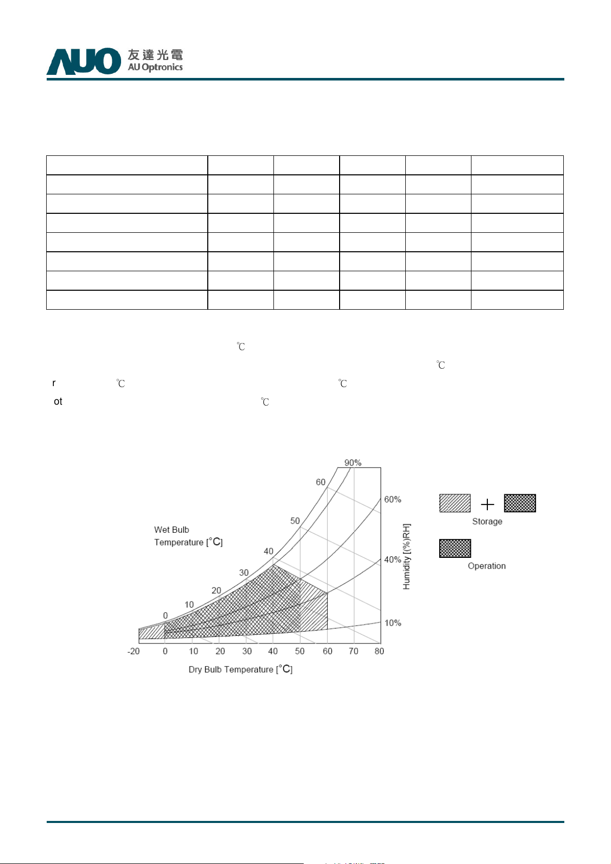
Operating Temperature TOP 0 +50 [oC] Note 2
Operating Humidity HOP 10 90 [%RH] Note 2
Storage Temperature TST -20 +60 [oC] Note 2
Storage Humidity HST 10 90 [%RH] Note 2
Panel Surface Temperature PST 65 [oC] Note 3
Note 1: Duration:50 msec.
Note 2 : Maximum Wet-Bulb should be 39 and No condensation.℃
Rev. 0.2
The relative humidity must not exceed 90% non-condensing at temperatures of 40 or less. At temperatures
greater than 40 , the wet bulb temperature must not exceed 39 .
Note 3: Surface temperature is measured at 50℃ Dry condition
℃ ℃
℃
© Copyright AU Optronics Corp. 2013 All Rights Reserved. Page 5 / 32
P460HVN01.2 Product Specification
Rev. 0.2
3. Electrical Specification
The P460HVN01.2 requires two power inputs. One is employed to power the LCD electronics and to drive the
TFT array and liquid crystal. The second is employed for LED driver.
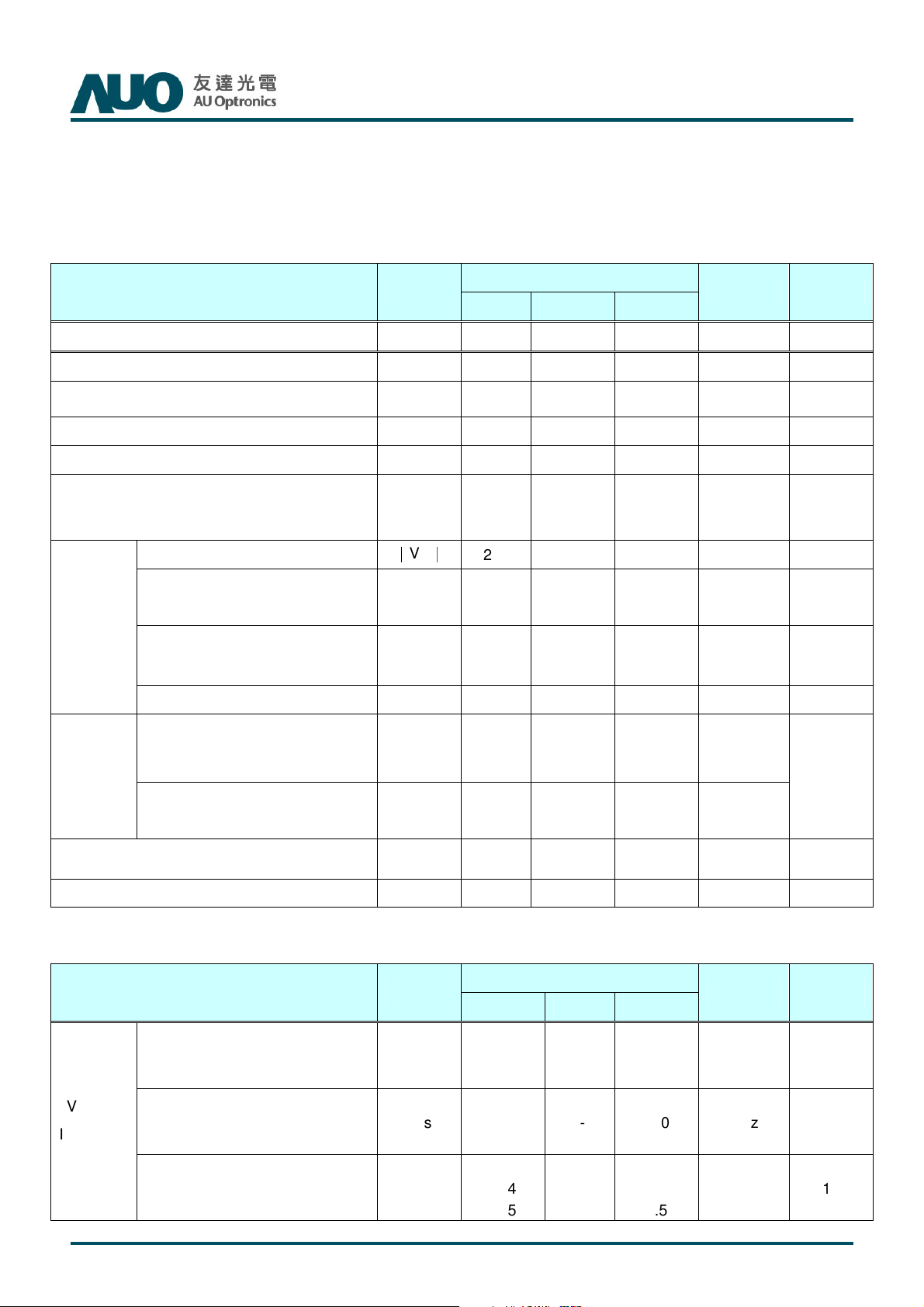
3.1.1 Electrical Characteristics
Parameter Symbol
LCD
Power Supply Input Voltage VDD 10.8 12 13.2 VDC
Power Supply Input Current IDD -- 0.9 1.08 A 1
Power Consumption PC -- 10.8 12.96 Watt 1
Inrush Current I
Permissible Ripple of Power Supply Input
Voltage
(for input power=12V)
Input Differential Voltage
Differential Input High Threshold
LVDS
Interface
Voltage
Differential Input Low Threshold
Voltage
Input Common Mode Voltage
RUSH
VRP -- -- VDD * 5%
∣
V
∣
ID
VTH +100 -- +300 mVDC 4
V
TL
V
ICM
Min. Typ. Max
- - 5.5 A 2
200 400 600 mVDC 4
-300 -- -100 mV
1.1
Value
1.25
Unit Note
mV
1.4
V
pk-pk
DC
DC
3
4
4
CMOS
Input High Threshold Voltage
Interface
Input Low Threshold Voltage
Backlight Power Consumption PBL --
Life Time(MTTF) -- 50000 -- 8
VIH
(High)
VIL
(Low)
2.7 -- 3.3 VDC
0 -- 0.6 VDC
123.1
W
3.1.2 AC Characteristics
Value
--
--
--
--
Fclk
+3%
200
0.4
0.5
Unit Note
MHz 9
KHz
ns
9
10
LVDS
Interface
Parameter Symbol
Receiver Clock : Spread
Spectrum
Modulation range
Receiver Clock : Spread
Spectrum
Modulation frequency
Receiver Data Input Margin
Fclk = 85 MHz
Fclk = 65 MHz
Fclk_ss
Fss
tRMG
Min. Typ. Max
Fclk
-3%
30
-0.4
-0.5
7
© Copyright AU Optronics Corp. 2013 All Rights Reserved. Page 6 / 32
s
µ
Note :
1. Test Condition:
(1) V
= 12.0V
DD
(2) Fv = Type Timing, 60Hz, 120Hz or Other
(3) F
= Max freq.
CLK
(4) Temperature = 25 ℃
(5) Test Pattern : White Pattern
2. Measurement condition : Rising time = 400us
90%
P460HVN01.2 Product Specification
Rev. 0.2
VVVV
DD
DD
DDDD
GND
GND
GNDGND
10%
400
400
400400
3. Test Condition:
(1) The measure point of V
is in LCM side after connecting the System Board and LCM.
RP
(2) Under Max. Input current spec. condition.
4. V
= 1.25V
ICM
L V D S -
V
IC M
L V D S +
G N D
|VID|
V
T H
|VID|
V
T L
0 V
|VID|
5. Do not attach a conducting tape to lamp connecting wire. If the lamp wire attach to conducting tape,
TFT-LCD Module have a low luminance and the inverter has abnormal action because leakage current
occurs between lamp wire and conducting tape.
6. The relative humidity must not exceed 80% non-condensing at temperatures of 40 or less. At
temperatures greater than 40 , the wet bulb temperature must not exceed 39 . When operate at low
℃ ℃
temperatures, the brightness of LED will drop and the life time of LED will be reduced.
7. The measure points of V
and V
IH
are in LCM side after connecting the System Board and LCM.
IL
© Copyright AU Optronics Corp. 2013 All Rights Reserved. Page 7 / 32
℃
P460HVN01.2 Product Specification
8. The lifetime (MTTF) is defined as the time which luminance of the LED is 50% compared to its original
value. [Operating condition: Continuous operating at Ta = 25±2℃, for single lamp/LED only.]
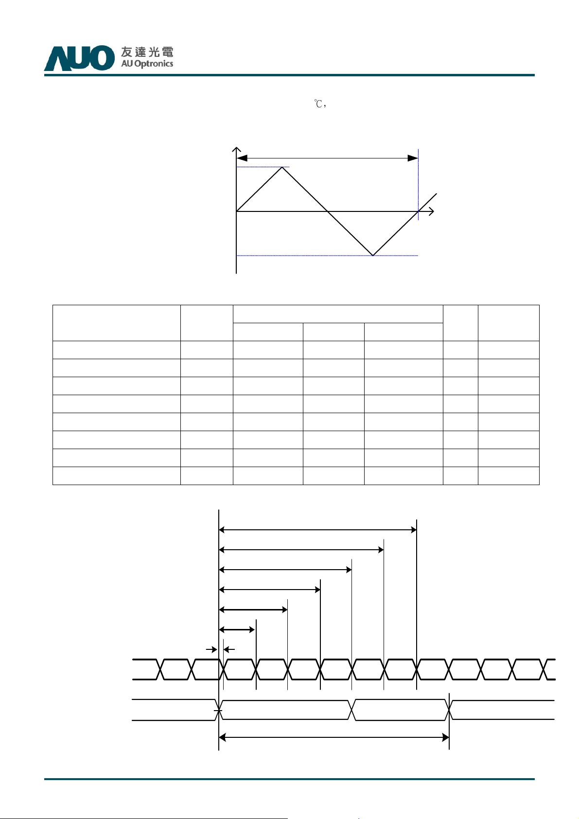
9. LVDS Receiver Clock SSCG (Spread spectrum clock generator) is defined as below figures
1111////FFFF
SS
SS
SSSS
Fclk
Fclk____ss
FclkFclk
ss((((max
ssss
Fclk
Fclk
FclkFclk
Fclk
Fclk____ss
FclkFclk
ss((((min
ssss
max))))
maxmax
min))))
minmin
10. Receiver Data Input Margin
Rev. 0.2
Parameter Symbol
Min Type Max
Input Clock Frequency Fclk Fclk (min) -- Fclk (max) MHz
Input Data Position0 tRIP1 -|tRMG| 0 |tRMG| ns
Input Data Position1 tRIP0 T/7-|tRMG| T/7 T/7+|tRMG| ns
Input Data Position2 tRIP6 2T/7-|tRMG|
Input Data Position3 tRIP5 3T/7-|tRMG|
Input Data Position4 tRIP4 4T/7-|tRMG|
Input Data Position5 tRIP3 5T/7-|tRMG|
Input Data Position6 tRIP2 6T/7-|tRMG|
Rating
Unit
2T/7 2T/7+|tRMG| ns
3T/7 3T/7+|tRMG| ns
4T/7 4T/7+|tRMG| ns
5T/7 5T/7+|tRMG| ns
6T/7 6T/7+|tRMG| ns
tRIP2
tRIP3
tRIP4
tRIP5
Note
T=1/Fclk
tRIP6
tRIP0
tRIP1
LVDS-Rx
Input Data
Rx1 Rx0 Rx6 Rx5 Rx4 Rx3 Rx2 Rx1 Rx0 Rx6Rx2Rx3
LVDS-Rx
VVVV
=
= 0000VVVV
= =
diff
diff
Input Clock
diff diff
1/Fclk=T
© Copyright AU Optronics Corp. 2013 All Rights Reserved. Page 8 / 32
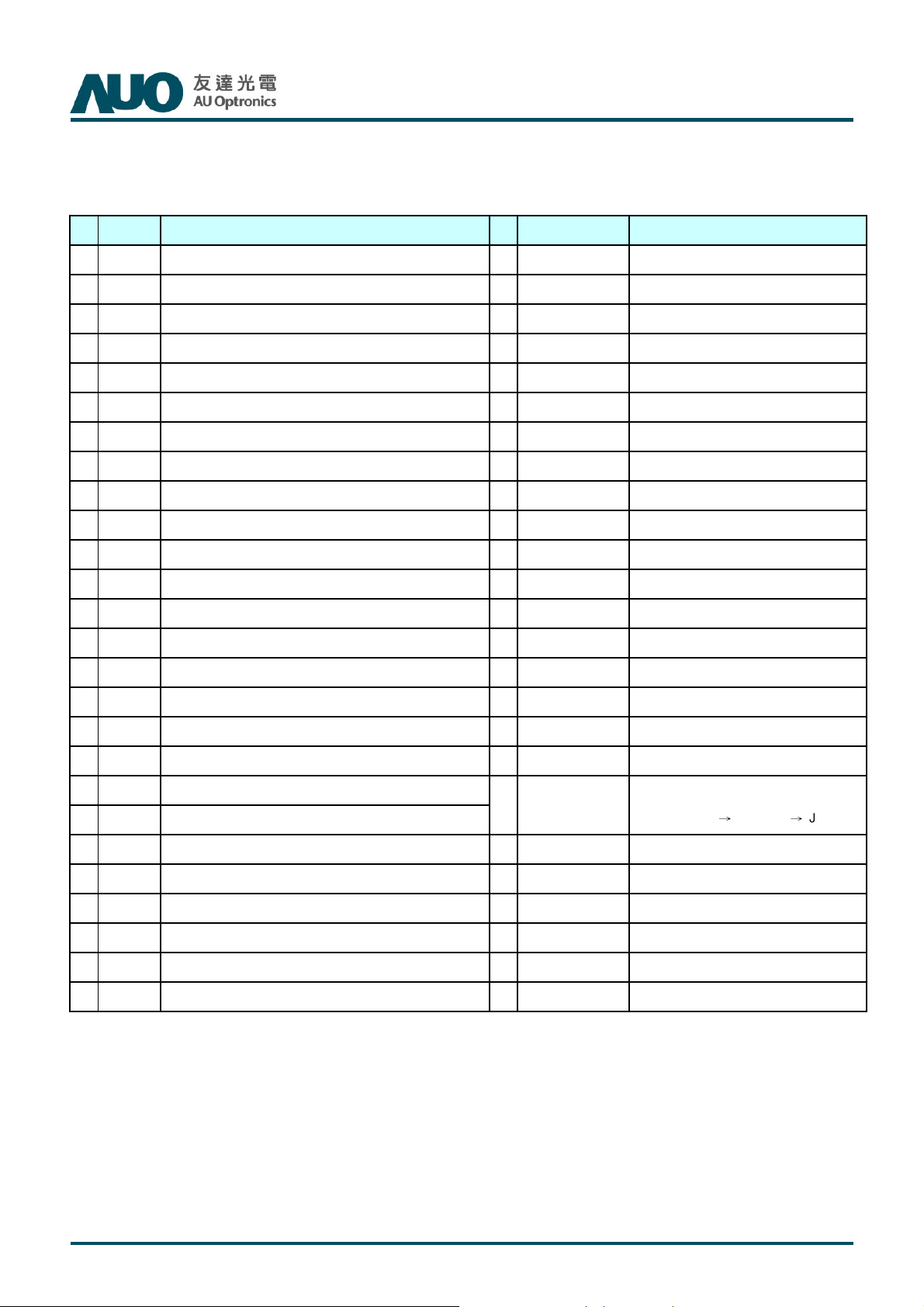
3.2 Interface Connections
LCD connector : FI-RE51S-HF (Manufactured by JAE);
Mating connector: FI-RE51HL (Manufactured by JAE)
P460HVN01.2 Product Specification
Rev. 0.2
PIN Symbol
1 VCC 12V Power Supply 27
2 VCC 12V Power Supply 28
3 VCC 12V Power Supply 29
4 VCC 12V Power Supply 30
5 VCC 12V Power Supply 31
6 GND GND 32
7 GND GND 33
8 GND GND 34
9 GND GND 35
10 RXON0
11 RXOP0
12 RXON1
13 RXOP1
14 RXON2
15 RXOP2
LVDS Odd pixel data input pair 0(-) 36
LVDS Odd pixel data input pair 0(+) 37
LVDS Odd pixel data input pair 1(-) 38
LVDS Odd pixel data input pair 1(+) 39
LVDS Odd pixel data input pair 2(-) 40
LVDS Odd pixel data input pair 2(+) 41
Description PIN
Symbol Description
RXEN1 LVDS Even pixel data input pair 1(-)
RXEP1 LVDS Even pixel data input pair 1(+)
RXEN2 LVDS Even pixel data input pair 2(-)
RXEP2 LVDS Even pixel data input pair 2(+)
GND GND
RXENCLK LVDS Even pixel clock input pair(-)
RXEPCLK LVDS Even pixel clock input pair(+)
GND GND
RXEN3 LVDS Even pixel data input pair 3(-)
RXEP3 LVDS Even pixel data input pair 3(+)
RXEN4 LVDS Even pixel data input pair 4(-)
RXEP4 LVDS Even pixel data input pair 4(+)
GND GND
NC No connected
Reserved AUO Internal Use Only
16 GND GND 42
17 RXONCLK
18 RXOPCLK
19 GND GND
20 RXON3
21 RXOP3
22 RXON4
23 RXOP4
24 GND GND 49
25 RXEN0
26 RXEP0
LVDS Odd pixel clock input pair(-) 43
LVDS Odd pixel clock input pair(+) 44
LVDS Odd pixel data input pair 3(-)
LVDS Odd pixel data input pair 3(+) 46
LVDS Odd pixel data input pair 4(-) 47
LVDS Odd pixel data input pair 4(+) 48
LVDS Even pixel data input pair 0(-) 50
LVDS Even pixel data input pair 0(+) 51
45
NC No connected
NC No connected
NC No connected
Select LVDS data order:
LVDSORD
High or NC → NS, Low → JEIDA
NC No connected
NC No connected
NC No connected
Reserved AUO Internal Use Only
Reserved AUO Internal Use Only
Reserved AUO Internal Use Only
Note 1: All GND (ground) pins should be connected together and should also be connected to the LCD’s
metal frame.
Note 2: All VDD (power input) pins should be connected together.
Note 3: All NC (no connection) pins should be open without voltage input.
© Copyright AU Optronics Corp. 2013 All Rights Reserved. Page 9 / 32
P460HVN01.2 Product Specification
Rev. 0.2
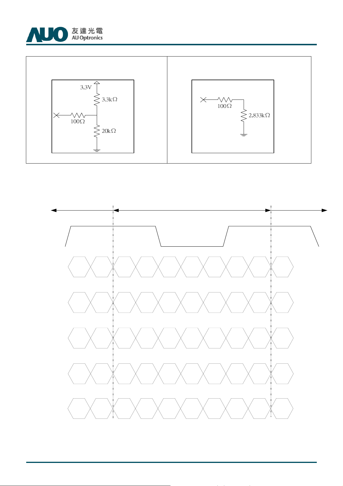
Note * : Open/High(3.3V)
LVDS Option = High/OpenNS
Previous C ycle Current Cycle Next Cycle
Previous C ycle Current Cycle Next Cycle
Previous C ycle Current Cycle Next Cycle Previous C ycle Current Cycle Next Cycle
Note ** : Open/Low(GND)
Clock
Clock
ClockClock
CHx
CHx____0000++++
CHxCH x
CHx
CHx____0000----
CHxCH x
CHx
CHx____1111++++
CHxCH x
CHx
CHx____1111----
CHxCH x
CHx
CHx____2222++++
CHxCH x
CHx
CHx____2222----
CHxCH x
CHx
CHx____3333++++
CHxCH x
CHx
CHx____3333----
CHxCH x
CHx
CHx____4444++++
CHxCH x
CHx
CHx____4444----
CHxCH x
DEBBBB2222BBBB3333 BBBB4444BBBB5555NA
DEDE
NARRRR6666RRRR7777 GGGG6666GGGG7777BBBB6666 RRRR7777
NANA
NARRRR8888RRRR9999 GGGG8888GGGG9999BBBB8888 RRRR9999
NANA
NA DE
NANA
NA BBBB3333
NANA
RRRR0000RRRR5555 GGGG0000GGGG0000RRRR0000RRRR1111 RRRR2222RRRR3333RRRR4444 RRRR1111
GGGG1111BBBB0000 BBBB1111BBBB1111GGGG1111GGGG2222 GGGG3333GGGG4444GGGG5555 GGGG2222
BBBB2222NA
RRRR6666BBBB7777 NA
RRRR8888BBBB9999 NA
DEDE
DEDE
NANA
NANA
NANA
NANA
Note: x = 1, 2, 3, 4…
© Copyright AU Optronics Corp. 2013 All Rights Reserved. Page 10 / 32
 Loading...