

Page 1

AC4830xC-C VoPP
Voice over Packet Processor
Data Book
Revision 1.0
Catalog Number LTRT-00060
US: AudioCodes Inc, 2841 Junction Ave, Suite 114, San Jose, CA 95134.
International: AudioCodes Ltd, 4 HaHoresh Rd, PO Box 14, Yehud 56470, Israel.
Tel: 408-577-0488 –- Fax: 408-577-0492
Tel: +972-3-539 4000 –- Fax: +972-3-539 4061
Technical Support: support@audiocodes.com
Page 2

Page 3

AC4830xC-C Data Book General
About this Data Book
Purpose and Scope
This Data Book describes the hardware and timing characteristics, applications and use
of the AC4830xC-C VoPP, Voice over Packet Processors, from AudioCodes Ltd. It is
designed for reading by any regular User without specialist skills but familiar with the
applications, products and services of AudioCodes Ltd.
Structure of this Manual
The Data Book has the following sections, which will help you to find the information
you need:
For Information on: Look at Chapter:
Release Notes, Notices and Warranty
Contents, Figures and Tables
Overview and Features
The Interfaces of the AC4830xC-C
Specification of the AC4830xC-C.
Applications, Evaluation System and Testing
PCM Highway Interface
Full Index of the Data Book
General
Contents
1. Introduction
2. Functional Interfaces
3. Chip Data and Timing
4. Application Notes
5. PCM Highway Interface
Index
Abbreviations and Terminology
Each abbreviation, unless widely used, is spelled out in full when first used, and only
Industry standard terms are used throughout this manual. The $ symbol indicates
hexadecimal notation.
Data Book Revision 1.0 - Release Note
This Data Book describes the latest Hardware and timing specifications for the
AC4830xC-C. The Software specifications are described in “AC4830xC-C Designer’s
Manual”, Catalog Number LTRT-00066.
Acknowledgements
NetFax® and NetCoder® are registered by AudioCodes Ltd.
AudioCodes acknowledges that various products referred to in this manual are subject
to copyright and/or trademark by their respective registered holders.
1
Revision 1.0
March 2000
Page 4

AudioCodes Ltd.
Notice
This Data Book describes the AC4830xC-C VoPP (Voice over Packet Processors) from
AudioCodes Ltd.
Information contained in this document is believed to be accurate and reliable at the time of
printing. However, due to ongoing product improvements and revisions, AudioCodes Ltd.
cannot guarantee accuracy of printed material after the Date Published nor can it accept
responsibility for errors or omissions.
For
Technical Support
e-mail: support@audiocodes.com
please contact:
In the US, fax 408-577-0492
In other countries, fax +972-3-539-4041
© Copyright 2000 AudioCodes Ltd.
This document is subject to change without notice.
Date Published: Mar-22-2000 Date Printed: Mar-22-2000
General Warranty.
AudioCodes Ltd. (hereinafter "AudioCodes") warrants that its Products (hereinafter "Products") shall
conform to Aud ioCodes’ published specificat ions for a peri od of one (1) year. The foregoing warrant y
does not apply to any Products which have been subject to misuse, neglect, accident, or modification or
which have been alt ered and ar e not capable of being tested by AudioCodes under its normal test
conditions. AudioCodes’ sole obligati on to the Purchaser (hereinaft er "Buyer") hereunder for Products
failing to meet the aforesaid warranty shall be, at AudioCodes' discretion, to replace the non-conforming
Products or issue t he Buyer credit for the purchase price of the non-conforming Products, where wi thin
the warrant y period: 1) AudioCodes has received written notice of any nonconformity; and 2) After
AudioCodes' writ ten authorization to do so the Buyer has returned the non-conformi ng Products to
AudioCodes, freight prepaid; and 3) AudioCodes has determined that the Products are non-conforming
and that such nonconformity is not a result of the Buyer’s conduct . No Products may be used in a life
support application. AudioCodes warrants that the Products sold hereund er shall at the t ime of shipmen t
be free and clear of liens and encumbrances. This warranty extends to t he Buyer only and may be invoked
by the Buyer for its customers. AudioCodes shall not accept warranty returns directly from the Buyer’s
customers or users of the Buyer’s products or devices. This warranty is in lieu of all othe r warranti es
whether express, impl ied or statutory i ncluding implie d warrant ies of merchantability or fitness for
particular purpose. AudioCodes shall not be l iabl e for damages due to delays in deliveries or use. In no
event shall AudioCodes be liable for any incidental or consequential damages due to breach of this
warranty or f or any infringement action initiated by a t hird part y. The Buyer’s sole remedy for any brea ch
shall be limited to the remedies set forth herein and shall not exceed the sale price for the Products.
AC4830xC-C VoPP
2
Catalog Number: LTRT-00060
Page 5

AC4830xC-C Data Book Contents
Table of Contents
1
Introduction 7
1.1 Overview.....................................................................................................................7
1.2 Features.......................................................................................................................8
2
Functional Description 11
2.1 Overview...................................................................................................................11
2.2 Interfaces...................................................................................................................13
2.2.1 Voice Interface................................................................................................14
2.2.2 PCM Clock Generator..................................................................................... 15
2.2.2.1 Examples of External Crystal Use:........................................................ 16
2.2.3 Host Port Interface ..........................................................................................17
2.2.4 Memory, I/O and CAS Interface......................................................................19
2.2.5 Channel Associated Signaling Port..................................................................21
2.2.6 Test Access Port.............................................................................................. 23
2.3 HPI on-chip Memory Map .........................................................................................24
2.4 Pin Description .......................................................................................................... 25
2.4.1 Signals and Pin-out 144-pin TQFP package ..................................................... 25
3
Chip Data and Timing 31
3.1 General Specifications ............................................................................................... 31
3.2 Electrical Characteristics and Operating Conditions....................................................32
3.2.1 Absolute Maximum Ratings over Specified Temp. Range................................32
3.2.2 Electrical Characteristics.................................................................................34
3.3 Timing Characteristics ............................................................................................... 35
3.3.1 Memory and I/O Interface Timing...................................................................35
3.3.1.1 Memory Read....................................................................................... 35
3.3.1.2 Memory Write......................................................................................37
3.3.1.3 General I/O Read Timing .....................................................................38
3.3.1.4 I/O Write Timing.................................................................................. 39
3.3.2 PCM Port Timing when External Codec Used .................................................40
3.3.2.1 PCM Port Receive Timing (using Codec) .............................................40
3.3.2.2 PCM Port Transmit Timing (using Codec) ............................................ 41
3.3.3 PCM Port Timing with Clock from PCM Framer............................................. 43
3.3.3.1 PCM Port Receive Timing (using PCM Framer) ................................... 43
3.3.3.2 PCM Port Transmit Timing (using PCM Framer) ....................................44
3.3.4 Host Port Interface Timing..............................................................................45
3.3.4.1 Host Port Interface Switching Characteristics........................................45
3.3.4.2 Host Port Interface Timing Requirements .............................................46
3.3.5 Reset Timing ..................................................................................................50
3.3.6 External Crystal Option................................................................................... 51
3.4 Packaging Specifications............................................................................................52
4
Applications 53
Revision 1.0
3
March 2000
Page 6

AudioCodes Ltd.
4.1 Interface Application Using PCM Framer/Codec ........................................................53
54
4.2 Interface Application Using Codec .............................................................................55
5
PCM Highway Interface 57
5.1 E1 PCM Highway......................................................................................................57
Index....... 59
AC4830xC-C VoPP
4
Catalog Number: LTRT-00060
Page 7

AC4830xC-C Data Book Contents
.
IST OF FIGURES
L
Figure 1-1: AC4830xC-C Chip.................................................................................................................... 7
Figure 2-1: AC4830xC-C Application Diagram for Each Channel ..............................................................12
Figure 2-2: AC4830xC-C Interface Diagram..............................................................................................13
Figure 2-3: AC4830xC-C Voice and Signaling Interface ............................................................................14
Figure 2-4: PLLMUL Register Contents.................................................................................................... 15
Figure 2-5: AC4830xC-C Host Port Interface (HPI) Signals ....................................................................... 17
Figure 2-6: AC4830xC-C Memory & I/O Interface Signals ........................................................................ 19
Figure 2-7: AC4830xC-C CAS Port Interface ............................................................................................ 21
Figure 2-8: E&M AB Signaling................................................................................................................. 21
Figure 2-9: AC4830xC-C Test Access Port Interface.................................................................................. 23
Figure 2-10: AC4830xC-C HPI Memory Map............................................................................................ 24
Figure 3-1: Memory Read Timing ............................................................................................................. 36
Figure 3-2: Memory Write Timing............................................................................................................. 37
Figure 3-3: I/O Read Timing ..................................................................................................................... 38
Figure 3-4: I/O Write Timing .................................................................................................................... 39
Figure 3-5: PCM Port Receive Timing Requirements (using Codec)........................................................... 41
Figure 3-6: PCM Port Transmit Timing Requirements (using Codec).......................................................... 42
Figure 3-7: PCM Port Receive Timing (using PCM Framer)....................................................................... 43
Figure 3-8: PCM Port Transmit Timing (using PCM Framer) ..................................................................... 44
Figure 3-9: Read/Write Access Without HRDY or HAS-............................................................................ 47
Figure 3-10: Read/Write Access Using HAS- Without HRDY.................................................................... 48
Figure 3-11: Read/Write Access with HRDY............................................................................................. 49
Figure 3-12: HRDY Signal when HCS- is Always Low.............................................................................. 50
Figure 3-13: Reset Timing......................................................................................................................... 51
Figure 3-14: Internal Clock Option............................................................................................................ 51
Figure 3-15: TQFP Packaging Specifications............................................................................................. 52
Figure 4-1: Typical Interface Application (Framer/Codec).......................................................................... 54
Figure 4-2: Typical Interface Application (Codec)...................................................................................... 56
Figure 5-1: E1 Timing............................................................................................................................... 57
Revision 1.0
5
March 2000
Page 8

AudioCodes Ltd.
List of Tables
Table 1-1: Available Features ..................................................................................................................... 9
Table 2-1: External Crystal Examples.........................................................................................................16
Table 2-2: HPI On-chip DPR Registers ......................................................................................................25
Table 2-3: AC4830xC-C Signals and Pin-out TQFP Package (continues on 6 pages) ...................................25
Table 3-1: General Specifications (continues on 2 pages)............................................................................31
Table 3-2: Characteristics over Recommended Operating Conditions..........................................................33
Table 3-3: Electrical Characteristics...........................................................................................................34
Table 3-4: Memory Read Timing Requirements .........................................................................................35
Table 3-5: Memory Write Timing Requirements.........................................................................................37
Table 3-6: I/O Read Timing Parameters .....................................................................................................38
Table 3-7: I/O Write Timing Parameters.....................................................................................................39
Table 3-8: PCM Port Receive Timing Requirements (using Codec).............................................................40
Table 3-9: PCM Port Transmit Switching Characteristics (using Codec)......................................................41
Table 3-10: PCM Port Transmit Timing Requirements (using Codec) .........................................................41
Table 3-11: PCM Port Receive Timing (using PCM Framer).......................................................................43
Table 3-12: PCM Port Transmit Switching Characteristics (using PCM Framer)..........................................44
Table 3-13: PCM Port Transmit Timing (using PCM Framer).....................................................................44
Table 3-14: Host Port Interface Switching Characteristics...........................................................................45
Table 3-15: Host Port Interface Timing Requirements.................................................................................46
Table 3-16: Timing Parameters for Reset....................................................................................................50
Table 3-17: TQFP Thermal Resistance Characteristics................................................................................52
AC4830xC-C VoPP
6
Catalog Number: LTRT-00060
Page 9

AC4830xC-C Data Book Chapter 1. Introduction
1 INTRODUCTION
1.1 Overview
The AC4830xC-C Voice over Packet Processors are state-of-the-art systems on a single
chip. They provide configurable, low-bit-rate voice compression and fax relay functions
for one or two independent voice and fax channels.
There are currently two members of the AC4830xC-C family:
• AC48302C-C - dual channels for client applications
• AC48301C-C - single channel for client applications.
Figure 1-1: AC4830xC-C Chip
Revision 1.0
ADVANTAGES
• Low cost
• Independent channel operation
• Toll quality voi ce compr ession
Robust bandwidth-saving fax relay
•
• Small foot pr int
• Low power consumption
7
March 2000
Page 10

AudioCodes Ltd.
APPLICATIONS
Cable telephony access devices
•
SOHO voice/data access devices
•
• DSL access devices
• Voice enabled set-top boxes
1.2 Features
• 1 or 2 channels of G.729A, G.723.1, G.727, G.726, G.711 and NetCoder
codecs
• T.38 or FRF.11 compliant fax relay at 2.4 – 14.4 kbps
Caller ID generation and detection
•
Automatic switching to PCM or ADPCM upon fax/data detection
•
• G.168-compliant 25 ms length, adaptive Echo Canceler
• High performance Voice Activity Detector (VAD) and Comfort Noise Generator
(CNG)
• DTMF detection and generation
Call Progress and User-defined tones detection and generation
•
• Clock and Frame Synchronization outputs to an external codec
• Parallel host processor interface
• Selectable µ-law/A-law PCM codec interface
• PCM highway interface for voice, fax and data
Input and output gain control
•
• E&M and AB signaling options
®
voice
AC4830xC-C VoPP
8
Catalog Number: LTRT-00060
Page 11

AC4830xC-C Data Book Chapter 1. Introduction
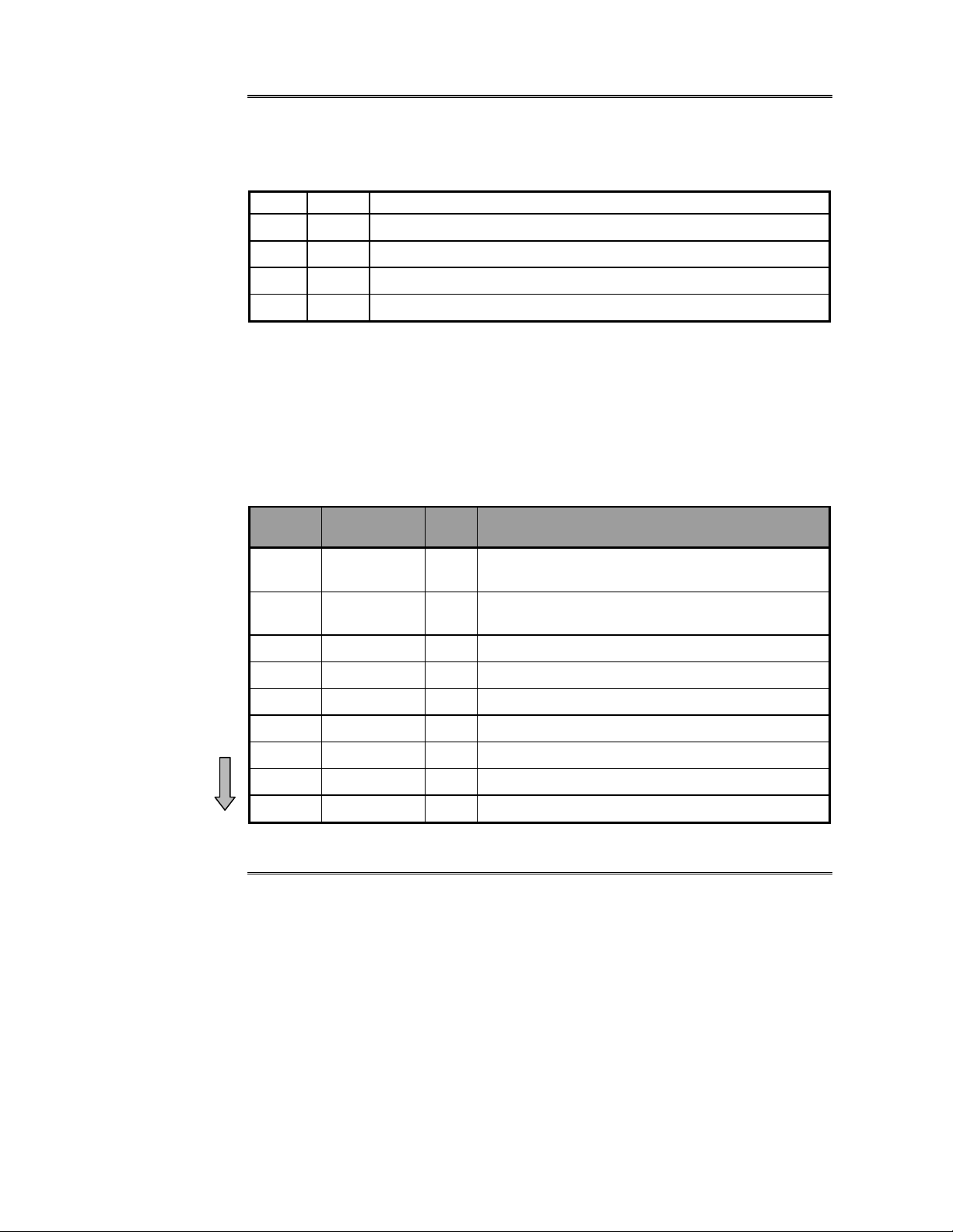
Table 1-1: Available Features
Feature AC48301C-C AC48302C-C
Number of Channels 1 2
G.711, G.726, G.727
G.723.1
G.729A
NetCoder
VAD and CNG
G.168 Echo Canceler
√√√√ √
√√√√ √
√√√√ √
√√√√ √
√√√√ √
√√√√ √
√√√
√√√
√√√
√√√
√√√
√√√
Echo Canceler Tail length (ms) 25 25
DTMF TIA 464B
MF-R1, MF-R2, SS-4, SS-5, AC15
Call progress, User defined
Bellcore Std. Caller ID generation &
√√√√ √
√√√√ √
√√√√ √
√√√√ √
√√√
√√√
√√√
√√√
detection
CAS E&M signaling
Input and output gain control
G3 Fax relay (T.38-compliant)
G3 Fax relay (FRF.11-compliant)
Automatic voice/fax/data switching
Bad Frame Interpolation (BFI)
µ/A-Law - PCM companding
Parallel Host Interface (8-bit)
√√√√ √
√√√√ √
√√√√ √
√√√√ √
√√√√ √
√√√√ √
√√√√ √
√√√√ √
√√√
√√√
√√√
√√√
√√√
√√√
√√√
√√√
Power supply - core (V) 1.8 1.8
Power supply - I/O (V) 3.3 3.3
ANSI-C source code driver
TQFP Package, 144 pins
√√√√ √
√√√√ √
√√√
√√√
Revision 1.0
9
March 2000
Page 12

AudioCodes Ltd.
Reader’s Notes
AC4830xC-C VoPP
10
Catalog Number: LTRT-00060
Page 13

AC4830xC-C Data Book Chapter 2. Functional Description
2 FUNCTIONAL DESCRIPTION
2.1 Overview
The AC4830xC-C voice processor family supports one or two low-bit-rate voice, fax or
data transmission channels. For voice transmission, the analog input is digitized using
an external PCM codec, input through the AC4830xC-C PCM interface, and
compressed to one of the supported bit rates. Fax transmissions are automatically
detected and demodulated by the integrated NetFax
detected and cause the AC4830xC-C to switch to PCM mode. The AC4830xC-C
transfers the resultant bit-stream (compressed voice or demodulated fax for all the
channels) in packets to the Host processor through the integral Host Port Interface.
The AC4830xC-C performs receive and transmit operations simultaneously. It receives
compressed, packetized speech data from a remote AC4830xC-C unit, through the Host
Port Interface. It decompresses speech data and transmits it through the PCM voice
interface. It also remodulates and transmits fax signals to the fax machine in analog
form. The fax relay process is transparent for the transmitting and the receiving fax
machines.
Many other built-in features support use of the AC4830xC-C in a wide range of
integrated voice, fax and data access, transmission and switching systems.
The features include voice activity detector (VAD), comfort noise generator (CNG) and
adaptive Echo Canceler. Additionally, both In-band Signaling (Detection and
Generation of: MF-R1, MF-R2, SS-4, SS-5, DTMF tones, Call Progress tones, Userdefined tones) and Channel Associated Signaling (E&M: A and AB) are provided.
2-1 on page 12 is a simplified Application Diagram for each of the AC4830xC-C
Figure
channels.
®
Engine. Data transmissions are
Revision 1.0
11
March 2000
Page 14

AudioCodes Ltd.
Figure 2-1: AC4830xC-C Application Diagram for Each Channel
Voice Compression
· G.729A CS-ACELP @ 8.0 kbps
· G.723.1 MP-MLQ @ 6.3 / 5 . 3 kbps
· G.726 ADPCM @ 16-40 kbps
· G.727 E-ADPCM @ 16-40 kbps
· G.711 PCM @ 64 kbps
· NetCoder @ 6.4-9.6 kbps
G3 FAX Relay
@2400-14400
Voice/Fax/Data
Discriminator/
MUX
Codec/
PCM Highway
Interface
Voice
Data ByPass
Baseband Processing
· VAD/CNG
· G.168 Echo Cancellation
· Call Progress
· DTMF Detection/Generation
· Bad Frame Interpolation
· User-defined Tones
· IBS / CAS / TAP
bps
Voice/Fax/Data
Packetizer/
MUX
Host I/F
Host
Processor
AC4830xC-C VoPP
12
Catalog Number: LTRT-00060
Page 15

AC4830xC-C Data Book Chapter 2. Functional Description
2.2 Interfaces
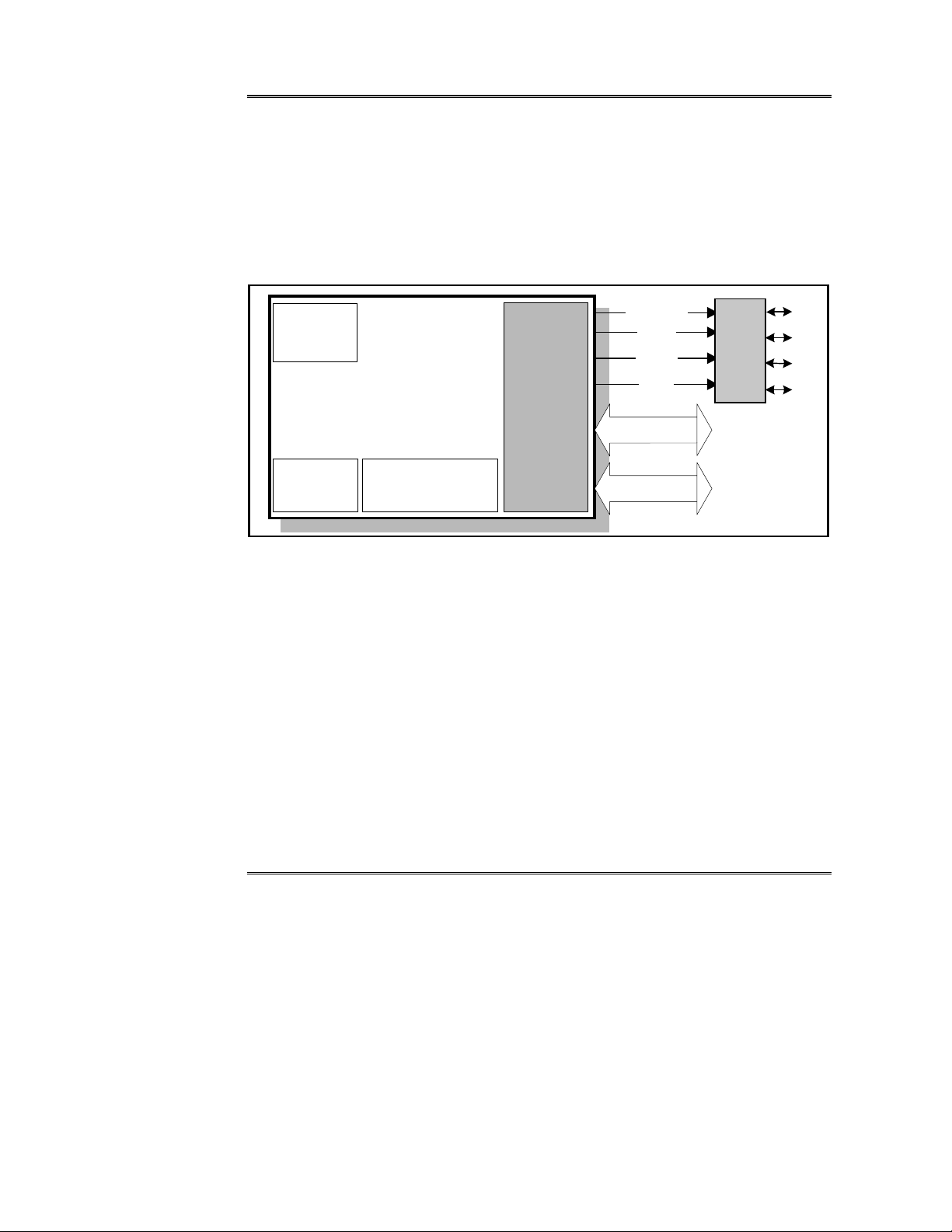
The various interfaces are shown below in Figure 2-2, and are described individually in
the following pages.
Figure 2-2: AC4830xC-C Interface Diagram
PCM
Crystal
Test I/F
Voice
Interface
PCM Clock
Generator
Test
Access
Port
AC4830xC-C
Host Port Interface
8-bit
Control
HOST
Memory &
I/O Interface
SIGEN-
IOS-
R/W-
MS-
16-bit
16-bit
Data
Address
Revision 1.0
13
March 2000
Page 16

AudioCodes Ltd.
2.2.1 Voice Interface
The AC4830xC-C uses the Voice Interface for input and output of uncompressed voice,
data and fax. It performs voice input and output as a 64 kbps companded A-Law or µLaw PCM.
The voice input is received through PCMIN, and the voice output is sent through
PCMOUT.
PCMCLK is a 2.048 MHz clock that can be generated internally from the AC4830xCC, or externally from a codec.
PCMFS is the PCM Frame Sync, that is generated every 125 µsec to comply with the
E1 transmission rate of 8,000 frames per sec. PCMFS can be generated internally from
the AC4830xC-C, or externally from a codec.
The User can attach the AC4830xC-C directly to a PCM highway.
Figure
PCM OUT
PCM IN
PCMCLK
PCMFS
2-3: AC4830xC-C Voice and Signaling Interface
Voice
Interface
Memory
& I/O
PCM Clock
Generator
AC4830xC-C
Interface
AC4830xC-C VoPP
TAP
HPI
14
Catalog Number: LTRT-00060
Page 17

AC4830xC-C Data Book Chapter 2. Functional Description
2.2.2 PCM Clock Generator
A built-in PCM Clock Generator enables the sourcing of an external codec device, with
the PCM Clock and PCM Frame Sync from the AC4830xC-C. The operation of the
PCM Clock Generator is fully controlled by the PCM Command Sequence, using the
PCMCLK control.
The PCM Clock Generator can use a wide range of CLKIN-Crystal clock inputs,
providing the User with a cost-effective solution. See Table 2-1 for some examples of
external crystals. The internal circuitry derives the AC4830xC-C working clock
(CLKOUT) from the AC4830xC-C clock input, and also the PCM Clock and the Frame
Sync characteristics.
The setting of the AC4830xC-C working clock is made by modifying the PLLMUL
field of the last word of the Kernel File, which is the PLLMUL Register, as shown in
Figure 2-4. The PLLMUL range is $00 to $0E. The working clock is indicated by the
CLKOUT signal.
Figure 2-4
:
PLLMUL Register Contents
Bit Number
Contents
Special care must be taken while modifying the file to avoid damaging its content and to
follow up the required working clock. The working clock range must be in the limits
98.304 to 100.00 MHz. The following section shows some examples of the use of
external crystals, based on the formula:
Please refer to AC4830xC-C Designer’s Manual, Catalog Number LTRT-00066, for
details of the PCM Command sequence.
15 14 13 12 11 10 9 8 7 6 5 4 3 2 1 0
PLLMUL $07 $FE
CLKOUT
[98.304 to 100.00]
=
CLKIN
x (PLLMUL+1)
[MHz]
Revision 1.0
15
March 2000
Page 18

AudioCodes Ltd.
2.2.2.1 Examples of External Crystal Use:
Table 2-1: External Crystal Examples
Crystal
Frequency MHz
20
25
16.384
12.288
8.192
2.048
PLLMUL
4 100
3 100
5 98.304
7 98.304
11 98.304
47 98.304
CLKOUT
MHz
Source for
2.048 MHz
Do Not Use
Do Not Use
Yes
Yes
Yes
Do Not Use
Notes
Default Value in Kernel File
See Section
PLLMUL must be <15
3.3.1 on page 35
-
-
-
AC4830xC-C VoPP
16
Catalog Number: LTRT-00060
Page 19

AC4830xC-C Data Book Chapter 2. Functional Description
2.2.3 Host Port Interface
The Host Port Interface (HPI) is an 8-bit parallel port used for communications between
the Host processor and AC4830xC-C. Both the Host processor and AC4830xC-C can
access and exchange information through the on-chip shared memory of the
AC4830xC-C. Please refer to the HPI on-chip Memory Map in Figure
An 8-bit data bus (HD0 to HD7) exchanges information with the Host. Because of its
16-bit word structure, the AC4830xC-C expects all transfers to consist of two
consecutive bytes. A dedicated pin (HI/LO) indicates whether the first or second byte is
being transferred.
Two control pins, HRS0 and HRS1, control Host access to the HPI. The Host can
access the internal control register and address the internal memory.
The Host can also interrupt the AC4830xC-C by writing to its internal control register.
Conversely, the AC4830xC-C can interrupt the Host with the HINT- signal, which the
Host can acknowledge and clear.
Figure
2-5 illustrates the signals of the Host Port Interface.
Figure 2-5: AC4830xC-C Host Port Interface (HPI) Signals
VOICE
Interface
2-10 on page 24.
Revision 1.0
TAP
HI/LO-
HPISEL-
AC4830xC-C
Host Port Interface
HR/W-
HRD-
HOST
HWR-
17
CS-
HAS-
MEMORY & I/O
Interface
HINT-
HRDY
HRS0-1
HD0-HD7
March 2000
Page 20

AudioCodes Ltd.
The AC4830xC-C has 2 data strobes (HRD- and HWR-), a read/write strobe (HR/W-),
and an address strobe (HAS-). These strobes establish a “glueless” interface with a
variety of industry-standard Host processors. The HPI is easily connected to the Host
with a multiplexed address/data bus, individual address/data buses, a data strobe, and
either one read/write strobe or two separate strobes for read and write.
An HPI ready pin (HRDY) is provided for Hosts that support an asynchronous input to
insert wait states. This is useful if the Host is capable of accessing data at a faster rate
than the maximum HPI access rate. The HRDY pin provides a convenient way to
automatically adjust the Host access rate (no software handshake is necessary).
Note: During Kernel Download, access timing to HPI is very different from the
access timing in other modes of operation.
AC4830xC-C VoPP
18
Catalog Number: LTRT-00060
Page 21
AC4830xC-C Data Book Chapter 2. Functional Description
2.2.4 Memory, I/O and CAS Interface
The AC4830xC-C requires one 64K x 16 SRAM device. For an example and
description of such a memory device, see Chapter 4, “Application Notes”.
The same Memory interface supports general purpose I/O ports. The I/O ports are
driven by 4-bit port In/Out buffers controlled by the SIGEN-. After the User issues the
Run command, the SIGEN- pin is asserted to “Low” level. The SRAM provides run-
time data storage. Figure
Figure 2-6: AC4830xC-C Memory & I/O Interface Signals
VOICE
Interface
AC4830xC-C
2-6 below, illustrates the signals of the Memory Interface.
A
A
B
B
MEMORY
SIGEN-
IOS-
R/W-
MS-
CAS
(E&M)
Port
& I/O
Interface
D0-D15
1
2
1
2
TAP
Revision 1.0
HPI
A0-A15
The AC4830xC-C handles E&M signals through an external I/O CAS (E&M) port, by
means of I/O strobe (IOS-), read/write (R/W-) and data bus lines, as shown above in
2-6.
Figure
It samples the E&M input (E) signals with a 1 ms resolution and transmits their values
to the remote side (receiving side) through the Host Port Interface (HPI) shown in
Section 2.2.3.
The AC4830xC-C receives from the remote side, the E&M output (M) signals, and
sends them to the I/O interface.
The output port is controlled by the SIGEN- pin, which keeps the I/O port in tri-state
until the processor enters the Active state. Signaling information is exchanged through
the data pins, and controlled by means of pins IOS- and R/W-.
MS- is the Memory strobe, and is used to indicate an external bus access to data or
program memory.
19
March 2000
Page 22

AudioCodes Ltd.
Figure 4-1 on page 54, shows a typical Interface Application when the clock is supplied
from the PCM Framer Codec, illustrating a typical design of an I/O port.
4-2 on page 56, shows a typical Interface Application when the clock is supplied
Figure
from the codec, illustrating a typical design of an I/O port.
Note: It is strongly recommended that pull-up/down resistors are added to
determine the correct output state during Initialization mode and Idle state
of operation. See Chapter 4, “Application Notes”.
AC4830xC-C VoPP
20
Catalog Number: LTRT-00060
Page 23

AC4830xC-C Data Book Chapter 2. Functional Description
2.2.5 Channel Associated Signaling Port
The Channel Associated Signaling (CAS, E&M) port is an external parallel port used
for signaling transfer between the AC4830xC-C and the Telephony Interface. This
external CAS port is connected to the AC4830xC-C via the SRAM’s low-order, 8-bit
data bus.
The signaling channel uses E&M (A and AB) signaling.
The CAS Port signals are shown in Figure
Figure 2-7: AC4830xC-C CAS Port Interface
VOICE
Interface
AC4830xC-C
TAP
The low ‘nibble’ (4-bit sub-field) of the signaling sample contains the E&M AB
signaling where the B bit is located in the Least Significant Bit within the sample, as
shown in Figure
The E&M ‘A’ represents 1-bit signaling information for each AC4830xC-C channel,
and the E&M ‘AB’ represents 2-bit signaling.
AC48301C-C - 1 channel
AC48302C-C - 2 channels
2-8, below.
Device
HPI
Figure 2-8: E&M AB Signaling
2-7 below:
MEMORY
& I/O
Interface
7 6 5 4 3 2 1 0
CAS
(E&M)
Port
Bit Number
B A
B2 B1 A2 A1
A
1
A
2
B
1
B
2
Revision 1.0
21
March 2000
Page 24

AudioCodes Ltd.
E&M A-signaling
When a single signaling bit is in use (E&M A-signaling), A
and A
corresponds to Channel 2.
2
E&M AB-signaling
When two signaling bits are in use (E&M AB-signaling), A
Channel 1, and A
2-8 on page 21.
and B2 are both allocated to Channel 2. See section 2.2.5 and Figure
2
corresponds to Channel 1,
1
and B1 are both allocated to
1
AC4830xC-C VoPP
22
Catalog Number: LTRT-00060
Page 25

AC4830xC-C Data Book Chapter 2. Functional Description
2.2.6 Test Access Port
The Test Access Port (TAP) is the boundary scan interface that is fully compliant with
the standard IEEE 1149.1.
Five pins are available for this interface:
- Test Clock. Free running clock with 50% duty cycle.
TCK
TDI
- Test Data Input. TDI is clocked into the selected internal port register on rising
edge of TCK.
- Test Data Output. The contents of the selected internal port register is shifted
TDO
out of TDO on falling edge of TCK. TDO is in high impedance state, except
when the scanning of data is in progress.
TMS
- Test Mode Select. Serial control input is clocked into the Test Access Port
internal controller on rising edge of TCK.
TRST-
- Test Reset. When high, gives the IEEE 1149.1 scan system control of the
operation of the AC4830xC-C. When low or not connected (pin is internally
pulled-down), the device operates in its functional mode, and the IEEE
standard 1149.1 signals are ignored.
See Figure 2-8 below for the TAP interface.
Figure 2-9: AC4830xC-C Test Access Port Interface
Revision 1.0
TCK
TDI
TDO
TMS
TRST-
VOICE
Interface
Test
Access
Port
AC4830xC-C
HPI
23
MEMORY
& I/O
I/F
March 2000
Page 26

AudioCodes Ltd.
S
2.3 HPI on-chip Memory Map
The on-chip memory is organized to facilitate the communication between the
AC4830xC-C and the Host processor. The AC4830xC-C operates in the following three
modes that together form the complete operational procedure:
Kernel download mode (BOOT)
•
• Program download mode
• Run time packet exchange
Figure 2-10: AC4830xC-C HPI Memory Map
HPID REGISTER
HD 0 to 7
1000h
Kernel Download Buffer
Boot Status Register
HI/LO-
HRS1
HRS0
HWR-
HRD-
HRW-
HAS-
HCS-
HRDY
HINT-
HPIA
Program Download Buffer
Number of Packets Register
Read Status Register
Write Status Register
Read Packet Buffer
Write Packet Buffer
HPI MEMORY BLOCK
104Ah
104Bh
104Ch
166Ch
166Dh
166Eh
166Fh
1670h
1737h
1738h
17FFh
HPIC
DSP DATA
DSP ADDRES
AC4830xC-C VoPP
24
Catalog Number: LTRT-00060
Page 27
AC4830xC-C Data Book Chapter 2. Functional Description
The HPI on-chip DPR Registers are shown in Table 2-2.
Table 2-2: HPI On-chip DPR Registers
HRS1 HRS0 Register Name
0 0 HPIC
0 1 HPID, with HPIA post-increment on read and pre-increment on write
1 0 HPIA
1 1 HPID, HPIA not affected
2.4 Pin Description
2.4.1 Signals and Pin-out 144-pin TQFP package
Table 2-3: AC4830xC-C Signals and Pin-out TQFP Package (continues on 6 pages)
VoPNP
Name
TQFP Pin # I/ O Description
PCMIN 45 I
PCMOUT 59 O/Z
PCMCLK 41 I/O PCM clock
PCMFS 43 I/O PCM frame sync
HD0 58 I/O/Z Host data bit 0
HD1 69 I/O/Z Host data bit 1
HD2 81 I/O/Z Host data bit 2
HD3 95 I/O/Z Host data bit 3
HD4 120 I/O/Z Host data bit 4
Revision 1.0
PCM data input. Sampled in on falling edge of
PCMCLK
PCM data output. Strobed out on rising edge of
PCMCLK
25
March 2000
Page 28
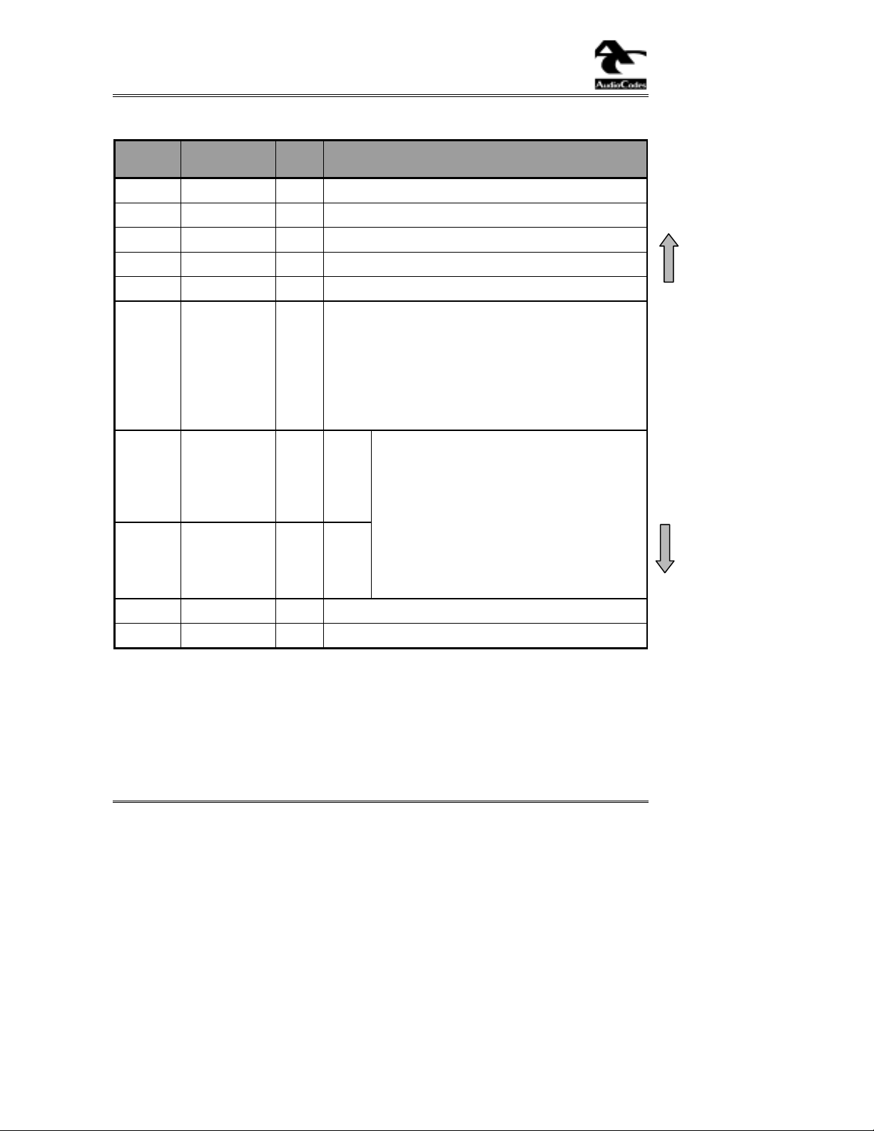
AudioCodes Ltd.
Table 2-3: AC4830xC-C Signals and Pin-out TQFP Package (continues on 6 pages)
VoPNP
Name
HD5 124 I/O/Z Host data bit 5
HD6 135 I/O/Z Host data bit 6
HD7 6 I/O/Z Host data bit 7
HINT- 51 O Host interrupt
HRDY 55 O Host ready
HR/W- 18 I Host read/write.
TQFP Pin # I/O Description
Hosts must drive HR/W- high to read from the Host
port interface.
Hosts must drive HR/W- low to write to the Host port
interface.
Hosts without an R/W- strobe must use an address
line.
HRD- 127 I
HWR- 129 I
HCS- 17 I Host chip select
HI/LO- 62 I High/low byte select
AC4830xC-C VoPP
Host
Read
Host
Write
•
The active low internal signal is the
XNOR of HRD- and HWR-.
•
Hosts with active low read and write
strobes must connect HRD- to the read
strobe and HWR- to the write strobe.
•
Hosts with active low data strobe must
connect it to HRD- and tie HWR- to +3.3V.
•
Hosts with active high data strobe must
connect it to HRD- and tie HWR- to GNDI.
26
Catalog Number: LTRT-00060
Page 29
AC4830xC-C Data Book Chapter 2. Functional Description
Table 2-3: AC4830xC-C Signals and Pin-out TQFP Package (continues on 6 pages)
VoPNP
Name
TQFP Pin # I/ O Description
HAS- 13 I Host address strobe.
•
Hosts with multiplexed address and data must
connect HAS- to their ALE pin. HI/LO-, HRS0,
HRS1 and HR/W- are latched on the HAS- falling
edge.
•
Hosts with separate address and data must
connect HAS- to +3.3 V. HI/LO-, HRS0, HRS1 and
HR/W- are latched on the HRD- or HWR- falling
edge when HAS- stays high.
HRS0 39 I Host register select 0
HRS1 46 I Host register select 1
HPISEL- 31 I
Host Port Interface select. Must be connected to
GNDI. (For future use
only
)
RESET- 98 I Master reset
SIGEN- 27 O Signaling enable
MS- 24 O Memory strobe
R/W- 23 O Memory read/write
IOS- 25 O I/O strobe
CLKOUT 94 O Clock out
XIN 97 I Crystal input
XOUT 96 O Crystal out
CLKMD2 78 I Must be connected to +3.3 V
TDO 85 O/Z IEEE standard 1149.1, test data output
TDI 86 I
IEEE standard 1149.1, test data input (Internal pullup)
TRST- 87 I IEEE standard 1149.1, test reset (Internal pull-down)
TCK 88 I IEEE standard 1149.1, test clock
Revision 1.0
27
March 2000
Page 30

AudioCodes Ltd.
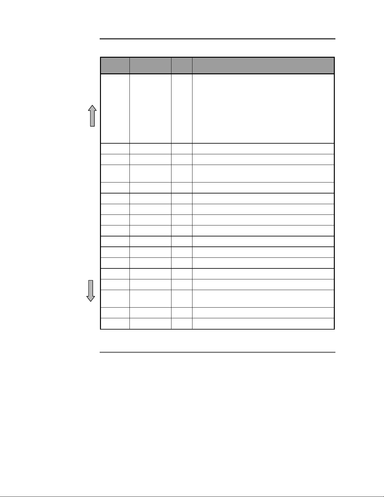
Table 2-3: AC4830xC-C Signals and Pin-out TQFP Package (continues on 6 pages)
VoPNP
Name
TQFP Pin # I/O Description
TMS 89 I
D0 99 I/O/Z External RAM Data 0
D1 100 I/O/Z External RAM Data 1
D2 101 I/O/Z External RAM Data 2
D3 102 I/O/Z External RAM Data 3
D4 103 I/O/Z External RAM Data 4
D5 104 I/O/Z External RAM Data 5
D6 113 I/O/Z External RAM Data 6
D7 114 I/O/Z External RAM Data 7
D8 115 I/O/Z External RAM Data 8
D9 116 I/O/Z External RAM Data 9
D10 117 I/O/Z External RAM Data 10
D11 118 I/O/Z External RAM Data 11
D12 119 I/O/Z External RAM Data 12
D13 121 I/O/Z External RAM Data 13
D14 122 I/O/Z External RAM Data 14
D15 123 I/O/Z External RAM Data 15
IEEE standard 1149.1, test mode select (Internal
pull-up)
A0 131 O External RAM Address 0
A1 132 O External RAM Address 1
A2 133 O External RAM Address 2
A3 134 O External RAM Address 3
A4 136 O External RAM Address 4
A5 137 O External RAM Address 5
AC4830xC-C VoPP
28
Catalog Number: LTRT-00060
Page 31

AC4830xC-C Data Book Chapter 2. Functional Description
Table 2-3: AC4830xC-C Signals and Pin-out TQFP Package (continues on 6 pages)
VoPNP
Name
TQFP Pin # I/ O Description
A6 138 O External RAM Address 6
A7 139 O External RAM Address 7
A8 140 O External RAM Address 8
A9 141 O External RAM Address 9
A10 5 O External RAM Address 10
A11 7 O External RAM Address 11
A12 8 O External RAM Address 12
A13 9 O External RAM Address 13
A14 10 O External RAM Address 14
A15 11 O External RAM Address 15, Must not be connected.
A16 105 O External RAM Address 16, Connect to A15 of SRAM.
RSRV1 19 I Must be connected to +3.3 V
RSRV2 30 I Must be connected to +3.3 V
RSRV3 32 I Connect to GNDI
RSRV4 42 I Must be connected to +3.3 V
RSRV5 44 I Must be connected to +3.3 V
RSRV6 47 I Must be connected to +3.3 V
RSRV7 63 I Must be connected to +3.3 V
RSRV8 64 I Must be connected to +3.3 V
RSRV9 65 I Must be connected to +3.3 V
RSRV10 67 I Must be connected to +3.3 V
RSRV11 77 I Must be connected to +3.3 V
RSRV12 54 I Must be connected to +3.3 V
RSRV13 79 I Must be connected to +3.3 V
Revision 1.0
29
March 2000
Page 32
AudioCodes Ltd.
Table 2-3: AC4830xC-C Signals and Pin-out TQFP Package (continues on 6 pages)
VoPNP
Name
RSRV14 49 I Must be connected to +3.3 V
TQFP Pin # I/O Description
RSRV15 83 I
RSRV16 84 I
RSRV19 92 I Must be connected to +3.3 V
RSRV20 66 I
RSRV21 48 I Must be connected externally to PCMCLK
RSRV22 53 I Must be connected externally to PCMFS
VDDI 4, 33, 56, 75,
112, 130
GNDC
VDDC
NC
3, 14, 34, 40
50, 57, 70, 76,
93, 106, 111,
128
16, 52, 68, 91,
125, 142
1, 2, 12, 15,
20, 21, 22, 26,
28, 29, 35, 36,
37, 38, 60, 61,
71, 72, 73, 74,
80, 82, 90,
107, 108, 109,
110, 126, 143,
144
Must be pulled up through a 4.7kΩ resistor to +3.3 V
Must be pulled up through a 4.7kΩ resistor to +3.3 V
Connect externally to HINT- and pull up thru 4.7kΩ
resistor
+3.3V for I/O pins
Ground
+1.8V for core CPU
Must Not Be Connected
AC4830xC-C VoPP
30
Catalog Number: LTRT-00060
Page 33

AC4830xC-C Data Book Chapter 3. Chip Data and Timing
3 CHIP DATA AND TIMING
3.1 General Specifications
Table 3-1: General Specifications (continues on 2 pages)
Characteristic Value
Number of Channels:
Voice Coders:
Voice Packetization:
Fax Relay Speeds:
Fax Modem Support:
Voice/fax Switching: Automatic.
Echo Cancelation:
DTMF Detection and
Generation:
VAD/CNG (Silence
Suppression):
VAD Response Time:
E&M Sampling Resolution:
Signaling Tone Generation:
Tone Generation Frequency:
Tone Generation Amplitude:
PCM Companding:
Analog Output Gain Control:
Dual independent voice/fax/data channels - AC48302C-C
Single voice/fax/data channels - AC48301C-C
G.723.1 MP-MLQ/ACELP at 6.3/5.3 kbps,
G.729/Annex A CS-ACELP
G.727 E-ADPCM at 16 to 40 kbps,
G.726 ADPCM at 16 to 40 kbps,
G.711 PCM at 64 kbps.
NetCoder
FRF.11 VoFR IA, or VoIP per RFC 1889.
Group 3 2400, 4800, 7200, 9600, 12000, 14400 bps.
V.17, V.21, V.27ter, V.29, V.33.
G.168; Max. echo path: 25 ms.
Detection Resolution: 10 ms, Generation Resolution: 1 ms,
16 digits, compliant with TIA 464B.
G.729 B for G.729A coders, and G.723.1A for G.723.1 coders
High Grade proprietary for G.711, G.726/727 & NetCoder
30 ms (max.) for G.723.1; 20 ms for NetCoder
10 ms for G.729A/G.729B; 5 ms for G.726/727 and G.711.
1 ms.
User-defined Dual -Tone Signaling.
Resolution: 1 Hz, Range: 0 to 4000 Hz.
Resolution: 1 dB, Range: -31 to 3 dBm.
A-law / µ-law (selectable).
± 31 dB in steps of 1 dB.
®
at 6.4 to 9.6 kbps.
1
at 8.0 kbps,
®
.
®
;
1
CS-ACELP = Conjugate Structure – Algebraic Code Excited Linear Predictive.
Revision 1.0
31
March 2000
Page 34

AudioCodes Ltd.
Table 3-1: General Specifications (continues on 2 pages)
Characteristic Value
Testability:
Package:
Temperature Range:
Power Supply: V
Current Consumption:
PCM loopback, coder loopback, test tone injection.
144-pin square TQFP.
Operation: 0° to 70° C, 32° to 158° F
Operating Case (T
Storage: -55° to 150° C, -67° to 302° F.
= +3.3 V ±10%; V
DDI
3.3V: ~20 mA (typical), 1.8V: ~61 mA (typical).
) -40° to 100° C, -40° to 212° F
c
= +1.8 V ±10%.
DDC
3.2 Electrical Characteristics and Operating
Conditions
3.2.1 Absolute Maximum Ratings over Specified Temp.
Range
Supply voltage range, V
Supply voltage range, V
Input voltage range - - -0.3 to 4.5 V
Output voltage range -- - -0.3 to 4.5 V
Operating case temperature range, TC
Storage temperature range, T
** All voltage values are with respect to VSS.
Note: Stresses beyond those listed under “Absolute Maximum Ratings” can
permanently damage the device. These are stress rating only, and
functional operation of the device at these or any other conditions beyond
those indicated above in Table 3-2, “Characteristics over Recommended
Operating Conditions”, is not implied. Exposure to Absolute Maximum
Rated conditions for extended periods can affect the device reliability.
AC4830xC-C VoPP
** - - -0.3 to 4.0 V
DDI
**- - -0.3 to 2.0 V
DDC
-40° to 100°C -40° to 212°F
STG
32
-55° to 150°C -67° to 302°F
Catalog Number: LTRT-00060
Page 35

AC4830xC-C Data Book Chapter 3. Chip Data and Timing
Table 3-2: Characteristics over Recommended Operating Conditions
General Characteristics Min Nom Max Unit
V
Supply voltage, I/O 3 3.3 3.6 V
DDI
V
Supply voltage, Core 1.7 1.8 2.00 V
DDC
VSS Supply voltage, GND 0 V
VIH High-level
input voltage
V
=3.3±0.3 V
DDI
VIL Low-level
input voltage
V
=3.3±0.3 V
DDI
IOH High-level output current -300
RESET-, RSRV20, XIN, PCMCLK,
TCLKR, RSRV21, TCLKX, HCS,
HRD, HWR, TDI, TMS, RSRV11,
RSRV13, CLKMD2
TCK, TRST-
All other inputs
RESET-, RSRV20, XIN, PCMCLK,
TCLKR, RSRV21, TCLKX, HCS,
HRD, HWR, TCK, RSRV11,
RSRV13, CLKMD2
All other inputs
2.2
2.5 V
2 V
-0.3
V
+ 0.3
DDI
+ 0.3
DDI
+ 0.3
DDI
0.6
-0.3 0.8
V
V
A
µ
IOL Low-level output current 1.5 mA
TC Operating case temperature
-40°
-40°
100°
212°
°
C
F
°
Revision 1.0
33
March 2000
Page 36

AudioCodes Ltd.
3.2.2 Electrical Characteristics
(Over Recommended Operating Case Temp. Range unless otherwise noted.)
Table 3-3: Electrical Characteristics
Parameter Test Conditions Min Typical Max Unit
VOH High-level output voltage V
=3.3+0.3V, IOH=MAX 2.4 V
DDI
VOL Low-level output voltage IOL=MAX 0.4 V
IIZ
Input
current, for
outputs in
high
impedance
II
Input
current
D[15:0],
HD[7:0]
All other
inputs
EXTCLK -40 40
TRST-
HPIEnable
Bus holders enabled,
=MAX, VI=VSS to V
V
DDI
V
=MAX,
DDI
V
O=VSS
to V
DDI
With internal
pulldown
With internal
V
I=VSS
to V
DDI
-175 175
DDI
-5 5
-5 300
-5 300
A
µ
µ
A
pulldown
TMS, TCK,
TDI, HPI
All other
With internal
pullups
-300 5
-5 5
input-only
pins
Ci Input capacitance 5 pF
Co Output capacitance 5 pF
* D = Data, HD = HPI Data
** All typical values are at V
*** All input and output voltage levels, except RESET- and XIN, are LVTTL-compatible.
=3.3V, TC=25°C (77°F).
DDI
AC4830xC-C VoPP
34
Catalog Number: LTRT-00060
Page 37

AC4830xC-C Data Book Chapter 3. Chip Data and Timing
3.3 Timing Characteristics
In all figures and tables in this section, the CLKOUT signal is derived directly from
F(CLKOUT) = 100 MHz, or when connected to a codec, F(CLKOUT) = 98.304 MHz.
Note: In the following Tables and Figures, Timing is over Recommended
Operating Conditions unless otherwise noted.
3.3.1 Memory and I/O Interface Timing
3.3.1.1 Memory Read
Table 3-4: Memory Read Timing Requirements
Parameter (units ns) Min Max
(11) Delay time, address valid from CLKOUT low
(17) Delay time, MS- low from CLKOUT low
(19) Delay time, MS- high from CLKOUT low
(12) Hold time, address valid after CLKOUT low
(13) Access time, read data access from address valid
(18) Access time, read data access from MS- low
(14) Setup time, read data before CLKOUT low
(16) Hold time, read data after CLKOUT low
(15) Hold time, read data after address invalid
(20) Hold time, read data after MS- high
* Values derived from characterization data and not tested.
u
User selectable
Notes to Table 3-4:
(CI) = 1/ Clock frequency
1. t
c
2. t
(CO) = tc(CI) /N nsec (where N is the Multiplication Factor = PLLMUL)
c
3. H = 0.5 t
(CO)
c
Example for a 100 MHz clock
(CI) = 1/ Clock frequency = 1/20 MHz = 50 nsec
1. t
c
2. t
(CO) = tc(CI) /N nsec (where N is the Multiplication Factor)
c
so t
(CO) = 50 nsec/5 =10 nsec
c
3. H = 0.5 t
(CO) = 5 nsec
c
-2* 3
-1 3
-1 3
-2 3
3
2
6
-2
0
0
u
u
Revision 1.0
35
March 2000
Page 38

AudioCodes Ltd.
Example for a 16.384 MHz clock
(CI) = 1/16.384 nsec ≅61 nsec
1. t
c
2. t
(CO) = 61/6 nsec ≅ 10.166 nsec
c
3. H = 0.5 t
4. The true value of (13) is 2H-7
CLKOUT
(CO) ≅5.083 nsec
c
≅
3.166 nsec, and (18) is 2H-8 ≅2.166 nsec.
Figure 3-1: Memory Read Timing
A15-A0
D15-D0
MS-
R/W-
11
17
13
18
14
12
15
16
20
19
AC4830xC-C VoPP
36
Catalog Number: LTRT-00060
Page 39

AC4830xC-C Data Book Chapter 3. Chip Data and Timing
3.3.1.2 Memory Write
Figure 3-2: Memory Write Timing
CLKOUT
22
21
A15-A0
23
D15-D0
MS-
R/W-
24
27
30
31
25
29
28
32
Table 3-5: Memory Write Timing Requirements
Parameter (units ns) Min Max
(22) Delay time, address valid from CLKOUT high
(21) Delay time, address valid from CLKOUT low
(28) Delay time, MS- low from CLKOUT low
(24) Delay time, data valid from CLKOUT low
(29) Delay time, MS- high from CLKOUT low
(30) Delay time, R/W- low from CLKOUT high
(33) Delay time, R/W- high from CLKOUT high
(31) Delay time, MS- low after R/W- low *
(26) Hold time, write data valid after MS- high
(32) Pulse Duration, MS- low *
(27) Setup time, address valid before MS- low
(25) Setup time, write data valid before MS- high
(23) Hold Time, address valid after CLKOUT high m
* Values derived from characterization data and not tested.
I/O
In the case of a Memory write preceded by an I/O cycle
M
In the case of a Memory write preceded by a Memory write
26
33
-2* 3
-2* 3
-1* 3
0* 6
-1 3
-1 3
-1 3
H-2 H+1
H-3
2H-2
2H-2
2H-6
1 3
H+6
2H+5
I/O
I/O
Revision 1.0
37
March 2000
Page 40

AudioCodes Ltd.
3.3.1.3 General I/O Read Timing
Table 3-6: I/O Read Timing Parameters
Parameter (units ns) Min Max
(41) Access time, read data access from address valid 3H-7
(42) Access time, read data access from IOS- low 2H-7
(43) Setup time, read data before CLKOUT high 6
(45) Delay time, address valid from CLKOUT low -2 3
(46) Delay time, IOS- low from CLKOUT high -2 3
(47) Delay time, IOS- high from CLKOUT high -2 3
(48) Hold time, address after CLKOUT low 0 3
(49) Hold time, read data after CLKOUT high 0
(50) Hold time, read data after IOS- high 0
.
Figure 3-3: I/O Read Timing
CLKOUT
45
A15-A0
D15-D0
IOS-
R/W-
AC4830xC-C VoPP
48
41
46
42
38
43
Catalog Number: LTRT-00060
49
50
47
Page 41
AC4830xC-C Data Book Chapter 3. Chip Data and Timing
3.3.1.4 I/O Write Timing
Table 3-7: I/O Write Timing Parameters
Parameter (units ns) Min Max
(45) Delay time, address valid from CLKOUT low -2 3
(46) Delay time, IOS- low from CLKOUT high -2 3
(51) Delay time, write data valid from CLKOUT high H-5 H+8
(47) Delay time, IOS- high from CLKOUT high -2 3
(52) Delay time, R/W- low from CLKOUT low -1 3
(53) Delay time, R/W-high from CLKOUT low -1 3
(54) Hold time, address valid from CLKOUT low 0 3
(55) Hold time, write data after IOS- high H-3 H+7
(56) Setup time, write data before IOS- high H-7 H+1
(44) Setup time, address valid before IOS- low H-2 H+2
Figure 3-4: I/O Write Timing
CLKOUT
45
44
54
A15-A0
D15-D0
IOS-
R/W-
Revision 1.0
51
46
56
52
39
47
55
53
March 2000
Page 42
AudioCodes Ltd.
3.3.2 PCM Port Timing when External Codec Used
When the AC4830xC-C is connected to a Codec, then the following Figures and Tables
within the
whole of Section 3.3.2 must apply
3.3.2.1 PCM Port Receive Timing (using Codec)
Table 3-8: PCM Port Receive Timing Requirements (using Codec)
Parameter (units ns) Min Max
(61) Cycle time, PCM port clock 4883 488
(62) Fall time, PCM port clock* 8
(63) Rise time, PCM port clock* 8
(64) Pulse duration, PCM port clock low/ high* 59 (65) Setup time, PCMFS before PCMCLK falling edge** 1
(66) Hold time, PCMFS after PCMCLK falling edge** 3 #PCM Clock - 1
(67) Setup time, PCMIN before PCMCLK falling edge 0
(68) Hold time, PCMIN after PCMCLK falling edge 4
* Values are ensured by design but not tested.
3
Applies to F(PCMCLK) = 2.048 MHz only
** Timings for PCMCLK and PCMFS are given with polarity bits (CLKP and FSP) set to 0.
# This value is 6 ns less than the PCM clock cycle time in (61). Refer to the Designer’s Manual for the
PCM clock value.
. Otherwise, see Section 3.3.3
3
AC4830xC-C VoPP
40
Catalog Number: LTRT-00060
Page 43

AC4830xC-C Data Book Chapter 3. Chip Data and Timing
Figure 3-5: PCM Port Receive Timing Requirements (using Codec)
61
PCMCLK
PCMFS
PCMIN
65
66
64
64
67
68
62
63
3.3.2.2 PCM Port Transmit Timing (using Codec)
Table 3-9: PCM Port Transmit Switching Characteristics (using Codec)
Parameter (units ns) Min Max
(71) Disable time, PCMOUT after PCMCLK rising* -1 4
(72) Enable time, PCMOUT after PCMCLK rising* 0 7
(73) Hold time, PCMOUT valid after PCMCLK rising 0 7
* Values are derived from characterization data but not tested.
Table 3-10: PCM Port Transmit Timing Requirements (using Codec)
Parameter (units ns) Min Max
(61) Cycle time, PCM port clock 4883 488
(64) Pulse duration, PCM port clock low/ high** 242 246
** Values are ensured by design but not tested.
3
Applies to F(PCMCLK) = 2.048 MHz only
3
Revision 1.0
41
March 2000
Page 44

AudioCodes Ltd.
Figure 3-6: PCM Port Transmit Timing Requirements (using Codec)
61
64
PCMCLK
64
PCMFS
(INT)
72
73
71
PCMOUT
AC4830xC-C VoPP
42
Catalog Number: LTRT-00060
Page 45

AC4830xC-C Data Book Chapter 3. Chip Data and Timing
3.3.3 PCM Port Timing with Clock from PCM Framer
When the AC4830xC-C is
PCM Framer, then the following Figures and Tables within the whole of Section 3.3.3
must apply. Otherwise, see Section 3.3.2
3.3.3.1 PCM Port Receive Timing (using PCM Framer)
Table 3-11: PCM Port Receive Timing (using PCM Framer)
Parameter (units ns) Min Max
(61) Cycle time, PCM port clock 1223
(62) Fall time, PCM port clock* 8
(63) Rise time, PCM port clock* 8
(64) Pulse duration, PCM port clock low/ high* 37
(65) Setup time, PCMFS before PCMCLK falling edge** 1
(66) Hold time, PCMFS after PCMCLK falling edge** 3
(67) Setup time, PCMIN before PCMCLK falling edge 0
(68) Hold time, PCMIN after PCMCLK falling edge 4
* Values are ensured by design but not tested.
3
Applies up to 8.192 Mbps
** Timings for PCMCLK and PCMFS are given with polarity bits (CLKP and FSP) set to 0.
Figure 3-7: PCM Port Receive Timing (using PCM Framer)
connected to a Codec, but receives its clock from the
not
PCMCLK
PCMFS
PCMIN
Revision 1.0
65
61
66
64
64
67
68
62
63
43
March 2000
Page 46

AudioCodes Ltd.
3.3.3.2 PCM Port Transmit Timing (using PCM Framer)
Table 3-12: PCM Port Transmit Switching Characteristics (using PCM Framer)
Parameter (units ns) Min Ma x
(71) Disable time, PCMOUT after PCMCLK rising* 3 9
(72) Enable time, PCMOUT after PCMCLK rising* 3 11
(73) Hold time, PCMOUT valid after PCMCLK rising 3 11
* Values are derived from characterization data but not tested.
Table 3-13: PCM Port Transmit Timing (using PCM Framer)
Parameter (units ns) Min Max
(61) Cycle time, PCM port clock 122
(62) Fall time, PCM port clock** 8
(63) Rise time, PCM port clock** 8
(64) Pulse duration, PCM port clock low/ high** 37
(66) Hold time, PCMFS after PCMCLK falling edge 3 1
(65) Setup time, PCMFS before PCMCLK falling edge 1
** Values are ensured by design but not tested.
Figure 3-8: PCM Port Transmit Timing (using PCM Framer)
61
PCMCLK
65
PCMFS
PCMOUT
AC4830xC-C VoPP
66
64
64
73
72
62
63
71
44
Catalog Number: LTRT-00060
Page 47

AC4830xC-C Data Book Chapter 3. Chip Data and Timing
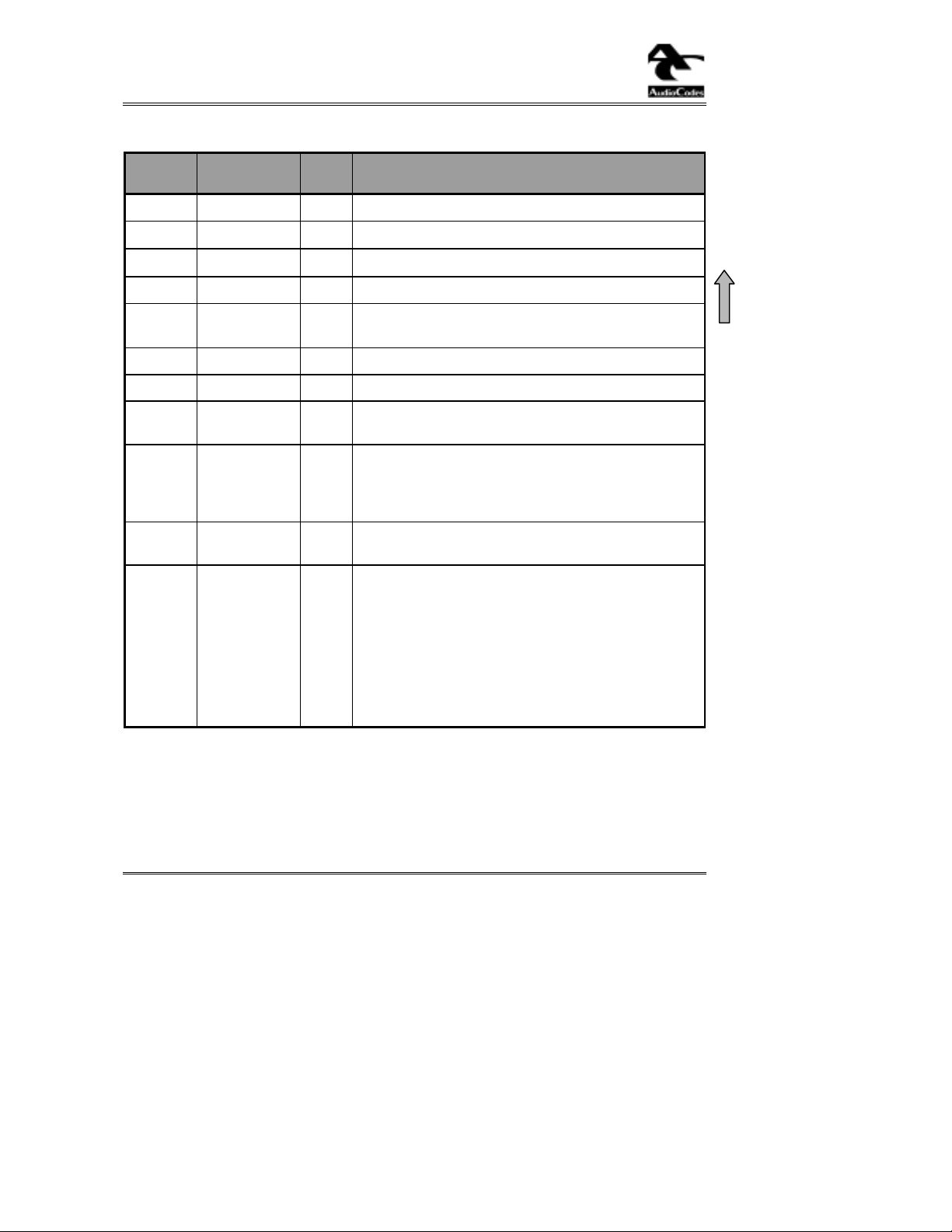
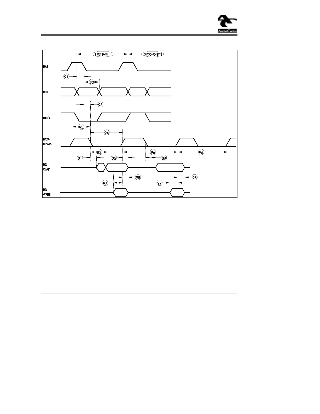
3.3.4 Host Port Interface Timing
3.3.4.1 Host Port Interface Sw itching Characteristics
Table 3-14: Host Port Interface Switching Characteristics
Parameter (units ns)
(81) Delay time, HCDS- low to HD valid
(82) Delay time, HRWR- falling to HD valid for first byte of a nonsubsequent read: max. 20 ns
During Kernel Download Mode (CLKOUT = 10 MHz):
case 1: if (95) <350 ns
case 2: if (95) >350 ns
Min Max
2 16
360
20**
During Other Modes (CLKOUT = 100 MHz):
case 1: if (95) <35 ns
case 2: if (95) >35 ns
(83) Delay time, HCDS- low to HD valid, second byte
(84) Delay time, HCDS- high to HRDY high (CLKOUT = 100 MHz)
(85) Setup time, HD valid before HRDY rising edge (CLKOUT =100 MHz)
(86) Hold time, HD valid after HCDS- rising edge
(87) Delay time, CLKOUT rising edge to HRDY high
(88) Delay time, HRWR- or HCS- high to HRDY low
(89) Delay time, CLKOUT rising edge to HIN change
45
20**
5 20
60**
5**
0 12*
10**
12**
15
* Values are derived from characterization data and not tested.
** Values are ensured by design but not tested.
Notes: For Table 3-14
1. HRS stands for HRS0, HRS1 and HR/W-; HRWR- refers to either HRD- or HWR-; HCDS- refers to
the logical OR of HCS- and HRWR-.
2. On Host read accesses to the HPI, the setup time of HD before the HCDS- rising edge depends on
the Host waveforms and cannot be specified here.
3. HRDY is not valid when the RESET is asserted (during kernel download).
Revision 1.0
45
March 2000
Page 48

AudioCodes Ltd.
3.3.4.2 Host Port Interface Timing Requirements
Table 3-15: Host Port Interface Timing Requirements
Parameter (units ns) Min Max
(91) Setup time, HRS, HR/W-, HI/LO- valid before HCDS- falling edge 10
(92) Hold time, HRS, HR/W-, HI/LO- valid after HCDS- falling edge 5
(93) Setup time, HAS low before HCDS- falling edge 12
(94) Pulse duration, HCDS- low 30*
(95) Pulse duration, HCDS- high 10
(96) Cycle time, HCDS- rising edge to next HCDS- rising edge
During Kernel Download Mode (CLKOUT = 10 MHz):
(see Figure 3-9, Figure 3-10)* *
During Other Modes (CLKOUT = 100 MHz):
case 1: when using HRDY (see Figure 3-11)
case 2: without using HRDY (see Figure 3-9, Figure 3-10)
(97) Setup time, HD valid before HCDS- rising edge 12
(98) Hold time, HD valid after HCDS- rising edge 3
* When the HRDY signal is not in use, during Run Mode of operation the Host must consistently meet
the 50 ns requirement.
* * When Run Mode not in active (during Download or Initialization Modes), the Host must consistently
meet the 500 ns requirement.
500
50
50
Notes: For Table 3-15
1. HRS stands for HRS0, HRS1 and HR/W-; HRWR- refers to either HRD- or HWR-; HCDS- refers to
the logical OR of HCS- and HRWR-.
2. On Host read accesses to the HPI, the setup time of HD before the HCDS- rising edge depends on
the Host waveforms and cannot be specified here.
3. HRDY is not valid when the RESET is asserted (during kernel download).
AC4830xC-C VoPP
46
Catalog Number: LTRT-00060
Page 49

AC4830xC-C Data Book Chapter 3. Chip Data and Timing
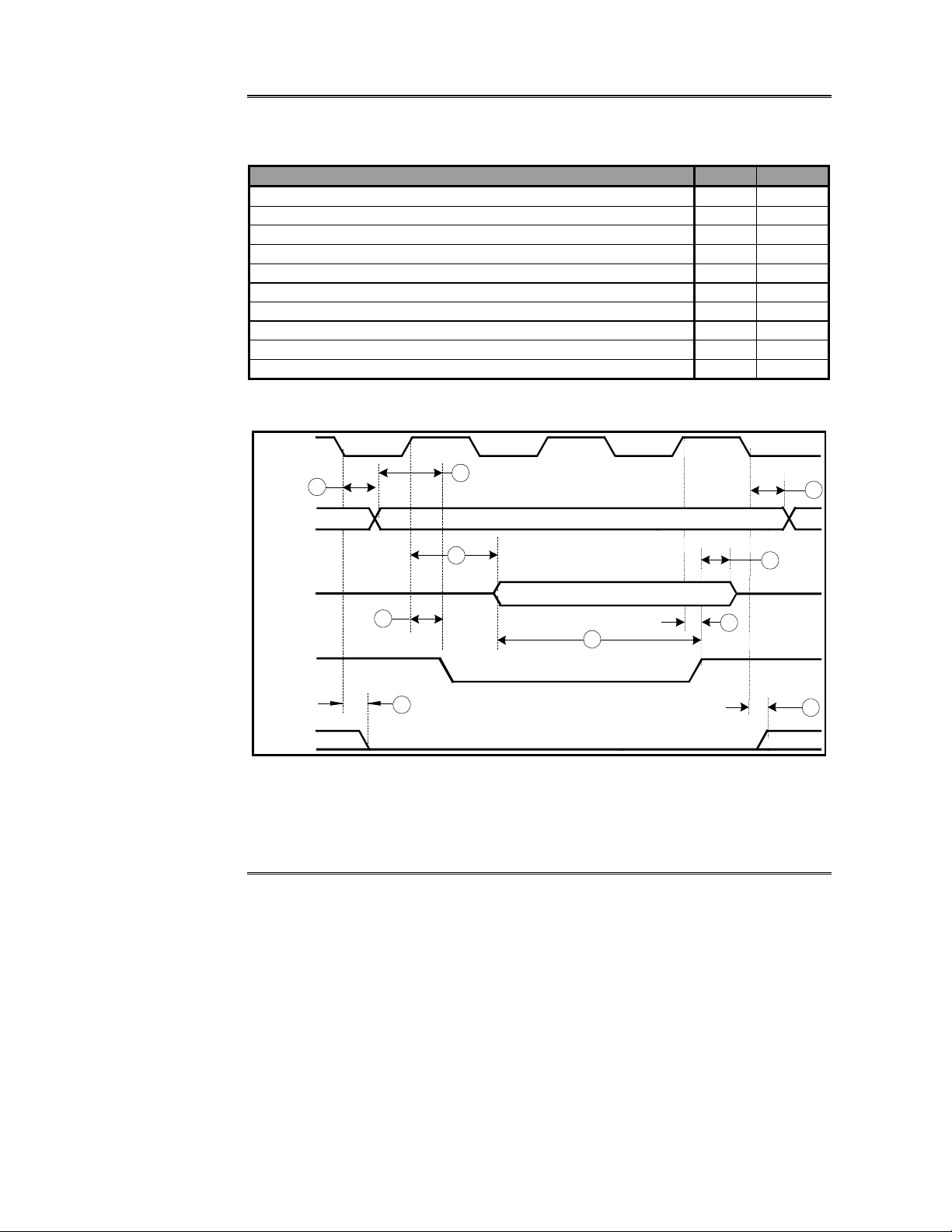
Figure 3-9: Read/Write Access Without HRDY or HAS-
Revision 1.0
Valid Valid
ValidValid
47
March 2000
Page 50
AudioCodes Ltd.
Figure 3-10: Read/Write Access Using HAS- Without HRDY
AC4830xC-C VoPP
48
Catalog Number: LTRT-00060
Page 51

V
V
AC4830xC-C Data Book Chapter 3. Chip Data and Timing
Figure 3-11: Read/Write Access with HRDY
Revision 1.0
ALID
VALID VALID
ALID
49
March 2000
Page 52

AudioCodes Ltd.
Figure 3-12: HRDY Signal when HCS- is Always Low
3.3.5 Reset Timing
Table 3-16: Timing Parameters for Reset
Parameter (units ns) Min Max
(101) Hold time, RESET- after CLKOUT low 0
(102) Pulse duration, RESET- low 1:
During Kernel Download Mode (CLKOUT=10 MHz): 2052
During Other Modes (CLKOUT=100 MHz): 252
(103) Setup time, RESET- before XIN low 5
(104) Setup time, RESET- before CLKOUT low 7 10
1
Values are derived from characterization data and are not tested.
2
For other frequencies, use the formula 4H+5
AC4830xC-C VoPP
50
Catalog Number: LTRT-00060
Page 53

AC4830xC-C Data Book Chapter 3. Chip Data and Timing
Figure 3-13: Reset Timing
3.3.6 External Crystal Option
Figure 3-14: Internal Clock Option
XOUT XIN
Crystal
Revision 1.0
C1
10pF
C2
10pF
A large variety of crystals can be used, examples being shown in Table
Please follow the guidelines for selecting the crystal value as explained in section
on page 15.
Connecting the selected crystal across XOUT and XIN, enables the internal oscillator.
The crystal must be capable of either fundamental or overtone operation, and parallel
resonant, with an effective series resistance of 30Ω, a power dissipation of 1 mW, and
specified for a load capacitance of 20 pF.
51
2-1 on page 16.
2.2.2
March 2000
Page 54

AudioCodes Ltd.
3.4 Packaging Specifications
The AC4830xC-C is packaged in a 144-pin TQFP, 20x20 mm body, shown below.
Figure 3-15: TQFP Packaging Specifications
Notes
1. All linear dimensions are in millimeters.
:
2. This drawing is subject to change without notice.
3. Falls within JEDEC MO-136.
Table 3-17: TQFP Thermal Resistance Characteristics
Parameter
RθJA
RθJC
AC4830xC-C VoPP
52
Catalog Number: LTRT-00060
°°°°C/W
56
5
Page 55

AC4830xC-C Data Book Chapter 4. Applications
4 APPLICATIONS
4.1 Interface Application Using PCM
Framer/Codec
Figure 4-1 on page 52 shows a typical Interface Application when the clock is supplied
from the PCM Framer/Codec.
Revision 1.0
53
March 2000
Page 56

AudioCodes Ltd.
Figure 4-1: Interface Application - External PCM Clocks
AC4830xC-C VoPP
54
Catalog Number: LTRT-00060
Page 57

AC4830xC-C Data Book Chapter 4. Applications
4.2 Interface Application Using Codec
Figure 4-2 on page 54 shows a typical Interface Application when the clock is supplied
from the Codec.
Revision 1.0
55
March 2000
Page 58
AudioCodes Ltd.
Figure 4-2: Interface Application - Driving a Codec
AC4830xC-C VoPP
56
Catalog Number: LTRT-00060
Page 59
AC4830xC-C Data Book Chapter 5. PCM Highway Interface
5 PCM HIGHWAY INTERFACE
The AC4830xC-C supports connection to E1 trunks.
An E1 system is composed of individual timeslots, each timeslot, or channel, consisting
of eight bits, numbered 1 to 8. Bit number 1 is the MSB and is transmitted first. Bit
number 8 is the LSB and is transmitted last.
5.1 E1 PCM Highway
In a single E1 system there are 32 such 8-bit timeslots numbered 0 to 31, and a 2.048
MHz clock drives the communications, as shown below in Figure
Figure 5-1: E1 Timing
PCMCLK
5-1.
PCMOUT
CHANNEL 31
(TIMESLOT 30)
MSBLSB MSBLSB
CHANNEL 32
(TIMESLOT 31)
CHANNEL 1
(TIMESLOT 0)
PCMFS
It should be noted that in the above case, PCMFS appears only in the 127
When working with more than one AC4830xC-C, starting the operation should follow
this order:
1. Download the kernel and program codes to all AC4830xC-C chips.
2. Switch each of the AC4830xC-C chips into Run mode and configure the Time Slots
allocation of each chip before the next chip is switched into Run mode. This
procedure must be followed for all of the chips to prevent any overlapping of the
Time Slots allocation (default value for all of the channels is the same).
3. Switch the required channels to the Active state.
The above procedure ensures that no data is overwritten in the PCM highway.
th
time slot.
Revision 1.0
57
March 2000
Page 60

AudioCodes Ltd.
Reader’s Notes
AC4830xC-C VoPP
58
Catalog Number: LTRT-00060
Page 61

AC4830xC-C Data Book Index
INDEX
16-bit Word Structure............................................................................................................................................ 17
64K x 16 SRAM Device. .......................................................................................................................................19
8-bit Data Bus..................................................................................... ....... ........ ...... ....... ......................................17
8-bit Parallel Port ..................................................................................................................................................17
ABCD bits for ABCD signaling .................................... ...... ....... ............................................................................ 21
Active State..................................................................................................................................................... 19, 57
address/data bus .................................................................................................................................................... 18
A-Law ............................................................................................................... ...... ....... ...... ...... ....... ...... ....... 14, 31
Analog Output Gain Control
Application Notes.................................... ...... ....... ...... ....... ...... ...... ....................................... ...... ....... ........ ...... 19, 20
CAS (Channel Associated Signaling) field
C
Input Capacitance.................................................................................................. ...... .................................. .... 34
i
CLKMD (External Oscillator/Crystal/Selection) Signal .................................. ...... ............................................. 27, 33
CLKOUT (Clock Out) Signal........................................................................................ 27, 35, 37, 38, 39, 45, 46, 50
CLKP (Clock Polarity) field
CNG (Comfort Noise Generator) field
C
Output Capacitance ................................ ...... ...... ....... ...... ......... ...... ...................................................................34
o
Control Pins .......................................................................................................................................................... 17
Current Consumption
Cycle Time
Data
Data Bus Lines................................................................................................ ...... ...... ....... ...... ....... ...... ...... ....... ... 19
Data Strobe ...... ...... ....... ...... ....... ..................................................................................................................... 18, 26
Delay Time ......................................................................................................................... ...........35, 37, 38, 39, 45
Disable Time
DTMF
..................................................................................................................................40, 41, 43, 44, 46
........................................................................................................................................................23, 28, 34
................................................................................................................................................41, 44
..........................................................................................................................................................11, 31
DTMF Detection and Generation
E&M .............................................................................................................................................................. 19, 31
E&M Sampling Resolution
E&M Signal.................................................................... ...... ....... ...... ....... ...... ...... ....... ...... ....... ...... ......................19
Echo Cancelation
Electrical Characteristics.................................................................................................................................. 32, 34
Enable Time
External Crystal Option ........ ....... ...... ....... ............................................................................................................. 51
External I/O Port ...... ...... ....... ................................................................................................................................ 19
Fax ............ ....... ...... ....... ...... ...... ....... ...... ......... ...... ......................................................................................... 11, 31
Fax at 12000 bps
Fax at 14400 bps
Fax at 2400 bps
Fax at 4800 bps
Fax at 7200 bps
Fax at 9600 bps
Fax Modem Support
Fax Relay
...............................................................................................................................................31
.................................................................................................................................................41, 44
...............................................................................................................................................31
...............................................................................................................................................31
.................................................................................................................................................31
.................................................................................................................................................31
.................................................................................................................................................31
.................................................................................................................................................31
.................................................................................................................................... ...... ....... ...... ..... 31
.............................................................................................................................31
........................................................................................ 11, 21
.................................................................................................................. 40, 43
................................................................................................ 11, 31
.........................................................................................................................................32
......................................................................................................... 11, 31
............................................................................................................................... 31
..........................................................................................................................................31
Revision 1.0
59
March 2000
Page 62

AudioCodes Ltd.
.................................................................................................................................... ...... ....... ...... ....... . 31
FRF.11
FRF.11 VoFR IA
FSP (Frame Sync Polarity) field
.................................................................................................................................... ...... ....... ...... ....... .... 31
G.711
G.711 PCM
G.726 ADPCM Vocoders at 16-40 kbps
G.727 E-ADPCM Vocoders
G.729/Annex A
Group 3 Fax
HAS- (Address Strobe) ....................................................................................................................................18, 27
HAS- (Host Address Strobe) Signal ........................................................................ ....... ...... ....... .......... 18, 27, 47, 48
.................................................................................................................................... ...... ....... ...... ....45, 46
HCDS-
HCS- (Host Chip Select) Signal............................................................................................................ 26, 45, 46, 50
HD (Host Data bit) Signal ............ ....... ....................................................................................................... 34, 45, 46
HI/LO- (High/Low Byte Select) Signal ............ ....... ...... ....... .......................................................................26, 27, 46
HINT- (Host Interrupt) Signal .............................. ...... ...... ....... ...... ....... ........ ...... ........................................17, 26, 30
Hold Time...................................................................................................35, 37, 38, 39, 40, 41, 43, 44, 45, 46, 50
HPI (Host Port Interface) field........................................................................................................ 17, 19, 27, 45, 46
HPISEL- (Host Port Interface Select) Signal.. ...... ................................................................................................... 27
HR/W- (Host Read/Write) Signal.................................................................................................... 18, 26, 27, 45, 46
HRD- (Host Read) Signal............................................................................................................... 18, 26, 27, 45, 46
HRDY (Host Ready) Signal.. ...... ....... ...... ....... ...... ...... ....... ...... ....... ...... ......................... 18, 26, 45, 46, 47, 48, 49, 50
HRDY (HPI Ready Pin)................................................................................................................................ ...... .. 18
HRS0 (Host Register Select 0) Signal ............................................................................................. 17, 25, 27, 45, 46
HRS1 (Host Register Select 1) Signal ............................................................................................. 17, 25, 27, 45, 46
HWR- (Host Write) Signal ............ ....... ...... ......... ................................................................................. 18, 26, 27, 45
Idle State....................................................................................................................... ....... ...... ...... .................... 20
IEEE 1149.1 Test Clock
IEEE 1149.1 Test Data Input
IEEE 1149.1 Test Data Output
IEEE 1149.1 Test Mode Select
IEEE 1149.1 Test Reset
IEEE 1149.1 Test Standards .... .............................................................................................................................. 23
I
Input Current (VI=VSS To VDD) ........................................................................................................................... 34
I
Input Current In High Impedance ...................................................................................................................... 34
I
IZ
INIT (Initialization).......................................................................................................... ....... ...... ....... ........ ....20, 46
Initialization Mode...........................................................................................................................................20, 46
Input Voltage Range ...... ...... ....... ...... ....... ...... ...................................................................... ....... ...... ......... ...... ..... 32
Internal Clock Option............................................................................................................... ............................. 51
Internal Control Register ....................................................................................................................................... 17
Internal Memory................................................................................................................................................... 17
High-Level Output Current ............................................ ....... ...... ....... ...... ...................................................33, 34
I
OH
Low-level Output Current .................................................................... ...... ....... ...... ....... ...... ...... ...................... 33
I
OL
Low-Level Output Current ......................... ....... ...... ...... ....... ...... ......... ...... ....... ...... ....... ...... ...... ....... ...... .....33, 34
I
OL
IOS- (I/O Strobe) Signal....................................................................................................................... 19, 27, 38, 39
JEDEC MO-136 ................................................................................................................................................... 52
Kernel Download ............................................................................................................... ............ 18, 24, 45, 46, 50
Low-Bit-Rate.................................................................................................................................................... 7, 11
LSB .................................................................................................................................. ...... ....... ...... ....... ...... ... 57
Modes of Operation ..................................................................................................................... ....... ...... ...... .18, 24
.............................................................................................................................................. 31
............................................................................................................40, 43
....................................................................................................................................................... 31
....................................................................................................... 31
........................................................................................................................... 31
................................................................................................................................................. 31
...................................................................................................................................................... 31
..........................................................................................................................23, 27
.................................................................................................................23, 27
..............................................................................................................23, 27
..............................................................................................................23, 28
...........................................................................................................................23, 27
AC4830xC-C VoPP
60
Catalog Number: LTRT-00060
Page 63

AC4830xC-C Data Book Index
MS (M Signaling) field.............................................................................................................................. 27, 35, 37
MS- (Memory Strobe) Signal ..................................................................................................................... 27, 35, 37
MSB ...... ...... ....... ...... ....... ...... ...... ....... ...... ......... ...... ....... ...... ................................................................................57
Multiplexed Address/Data Bus...............................................................................................................................18
NetCoder® Vocoder at 4.8 kbps to 9.6 kbps
On-chip Shared Memory........................................................................................................................................ 17
Operating Case Temperature Range........................................................................................................................32
Operating Conditions................................................................................................................................. 32, 33, 35
OR (Over-run) field
Output Voltage Range ...........................................................................................................................................32
Overview .... ...... ....... ...... ....... ...... ...... ....... ...... ....... ........ ...... ....... .......................................................................7, 11
Packaging .......... ...................................................................................................................................................52
PCM Clock ..................................................................................................................................................... 25, 40
PCM Companding
PCM Highway
PCM Loopback
PCM Port Clock
PCM Port Receive............................................................................................................................... 40, 41, 43, 44
PCM Port Transmit.......................................................................................................................................... 41, 42
PCMCLK (PCM Clock Input) Signal ........................................................................................25, 30, 40, 41, 43, 44
PCMFS (PCM Frame Sync Input) Signal...................................................................................25, 30, 40, 43, 44, 57
PCMIN (PCM Data Input) Signal.... ...... ..................................................................................................... 25, 40, 43
PCMOUT (PCM Data Output) Signal...... ...... ............................................................................................. 25, 41, 44
Pin Description...................................................................................................................................................... 25
Power Supply
Pulse Duration.................................................................................................................... 37, 40, 41, 43, 44, 46, 50
R/W- (Memory Read/Write) Signal..........................................................................18, 19, 26, 27, 37, 39, 47, 48, 49
RESET- (Master Reset) Signal............................................................................................................. 27, 33, 34, 50
Reset Timing................................................................................................................................................... 50, 51
Rise Time
Run Mode
Setup Time........................................................................................................ 35, 37, 38, 39, 40, 43, 44, 45, 46, 50
SIGEN- (Signaling Enable) Signal .............................................................. ...... ...... ....... ...... ....... ........ ...... ....... 19, 27
Signal Processing .............................................................................................................................. ........ ...... ...... 53
Signaling
Signaling Tone Generation
Signals and Pinout ................................................................................................................................................. 25
SRAM ............................................................................................................................................................19, 29
Storage Temperature..............................................................................................................................................32
Supply Voltage................................................................................................................................................ 32, 33
Switching Characteristics................................................................................................................. ...... ....... ... 41, 45
T
C
Test ................................................................................................................................................................ 23, 34
Testability
Theory of Operation ..............................................................................................................................................11
................................................................................................................................................ 40, 43, 44
.................................................................................................................................... ...... ....... .. 46, 57
......................................................................................................................................... 11, 19, 27, 31
Operating Case Temperature ............ ....... ...... ....... .............................................................................................33
.................................................................................................................................... ...... ....... ...... .... 32
.................................................................................................................................. 45, 46
.............................................................................................................................................31
...........................................................................................................................................14, 57
.................................................................................................................................... ...... ...... 32
............................................................................................................................... 40, 41, 43, 44
.....................................................................................................................................................32
................................................................................................................................31
TIA 464A DTMF Detection and Generation
Timing Characteristics...........................................................................................................................................35
Timing Parameters ............................................ ....... ...... ....... ...... ...... ....... ...... ....... ...... ...... ....... ...... ......... .. 38, 39, 50
Timing Parameters For Reset ............................................ ....... ...... ....... ...... ...... ....... ...... ....... ................... ...... ........ 50
Timing Requirements .....................................................................................................................35, 37, 41, 42, 46
.................................................................................................................................... ...... ....... ...... ....... ...... 31
Tone
Tone Generation
.................................................................................................................................................31
............................................................................................... 31
............................................................................................... 31
Revision 1.0
61
March 2000
Page 64

AudioCodes Ltd.
TQFP Packaging................... ...... ......... ...... ....... ...... ....... ...... ...... ....... ...... ....... ...... ...................................... 25, 32, 52
TS (Tri-state) field ............................................................................................................... ...... ....... ...... ...... ....... . 19
.................................................................................................................................... ...... ....... ...... ....... ...... 31
V.21
.................................................................................................................................... ...... ....... ...... ....... ...... 31
V.27
.................................................................................................................................... ...... ....... ...... ....... . 31
V.27ter
.................................................................................................................................... ...... ....... ...... ....... ...... 31
V.29
.................................................................................................................................... ...... ....... ...... ....... ...... 31
V.33
VAD (Voice Activity Detector) field
VAD Response Time
VDDC.......................................................................................................................................................30, 32, 33
VDDI.................................................................................................................................26, 27, 29, 30, 32, 33, 34
High-level Input Voltage...... ...... ..................................................................................................................... 33
V
IH
V
Low-level Input Voltage.................................................................................................................................. 33
IL
High-Level Output Voltage ............................................................................................................................ 34
V
OH
Voice Coders
Voice Packetization
Voice/Fax Switching
V
Low-level Output Voltage .............................................................................................................................. 34
OL
V
Supply Voltage............................................................................................................................................... 33
SS
XIN (Crystal/External Oscillator Input) Signal ................................................................................ 27, 33, 34, 50, 51
XOUT (Crystal Out) Signal.. ............................................................................................................................27, 51
........................................................................................................................................ 31
..................................................................................................................................................... 31
.................................................................................................................................... ...... . 31
......................................................................................................................................... 31
...................................................................................................11, 31
AC4830xC-C VoPP
62
Catalog Number: LTRT-00060
 Loading...