


查询TS68040 供应商
Features
• 26-42 MIPS Integer Performance
• 3.5-5.6 MFLOPS Floating-Point-Performance
• IEEE 754-Compatible FPU
• Independent Instruction and Data MMUs
• 4K bytes Physical Instruction Cache and 4K bytes Physical Data Cache Accessed
Simultaneously
• 32-bit, Nonmultiplexed External Address and Data Buses with Synchronous Interface
• User-Object-Code Compatibility with All Earlier TS68000 Microprocessors
• Multimaster/Multiprocessor Support via Bus Snooping
• Concurrent Integer Unit, FPU, MMU, Bus Controller, and Bus Snooper Maximize
Throughput
• 4G bytes Direct Addressing Range
• Software Support Including Optimizing C Compiler and UNIX
• IEEE P 1149-1 Test Mode (JTAG)
• f = 25 MHz, 33 MHz; V
• The Use of the TS88915T Clock Driver is Suggested
=5V±5%;PD=7W
CC
®
System V Port
Description
ThirdGeneration
32-bit
Microprocessor
The TS68040 is Atmel’s third generation of 68000-compatible, high-performance, 32bit microprocessors. The TS68040 is a virtual memory microprocessor employing
multiple, concurrent execution units and a highly integrated architecture to provide
very high performance in a monolithic HCMOS device. On a single chip, the TS68040
integrates a 68030-compatible integer unit, an IEEE 754-compatible floating-point unit
(FPU), and fully independent instruction and data demand-paged memory management units (MMUs), including 4K bytes independent instruction and data caches. A
high degree of instruction execution parallelism is achieved through the use of multiple independent execution pipelines, multiple internal buses, and a full internal
Harvard architecture, including separate physical caches for both instruction and data
accesses. The TS68040 also directly supports cache coherency in multimaster applications with dedicated on-chip bus snooping logic.
The TS68040 is user-object-code compatible with previous members of the TS68000
Family and is specifically optimized to reduce the execution time of compiler-generated code. The 68040 HCMOS technology, provides an ideal balance between speed,
power, and physical device size.
Figure 1 is a simplified block diagram of the TS68040. Instruction execution is pipelined in both the integer unit and FPU. Independent data and instruction MMUs control
the main caches and the address translation caches (ATCs). The ATCs speed up logical-to-physical address translations by storing recently used translations. The bus
snooper circuit ensures cache coherency in multimaster and multiprocessing
applications.
Screening
TS68040
• MIL-STD-883
• DESC. Drawing 5962-93143
• Atmel Standards
Rev. 2116A–HIREL–09/0 2
1
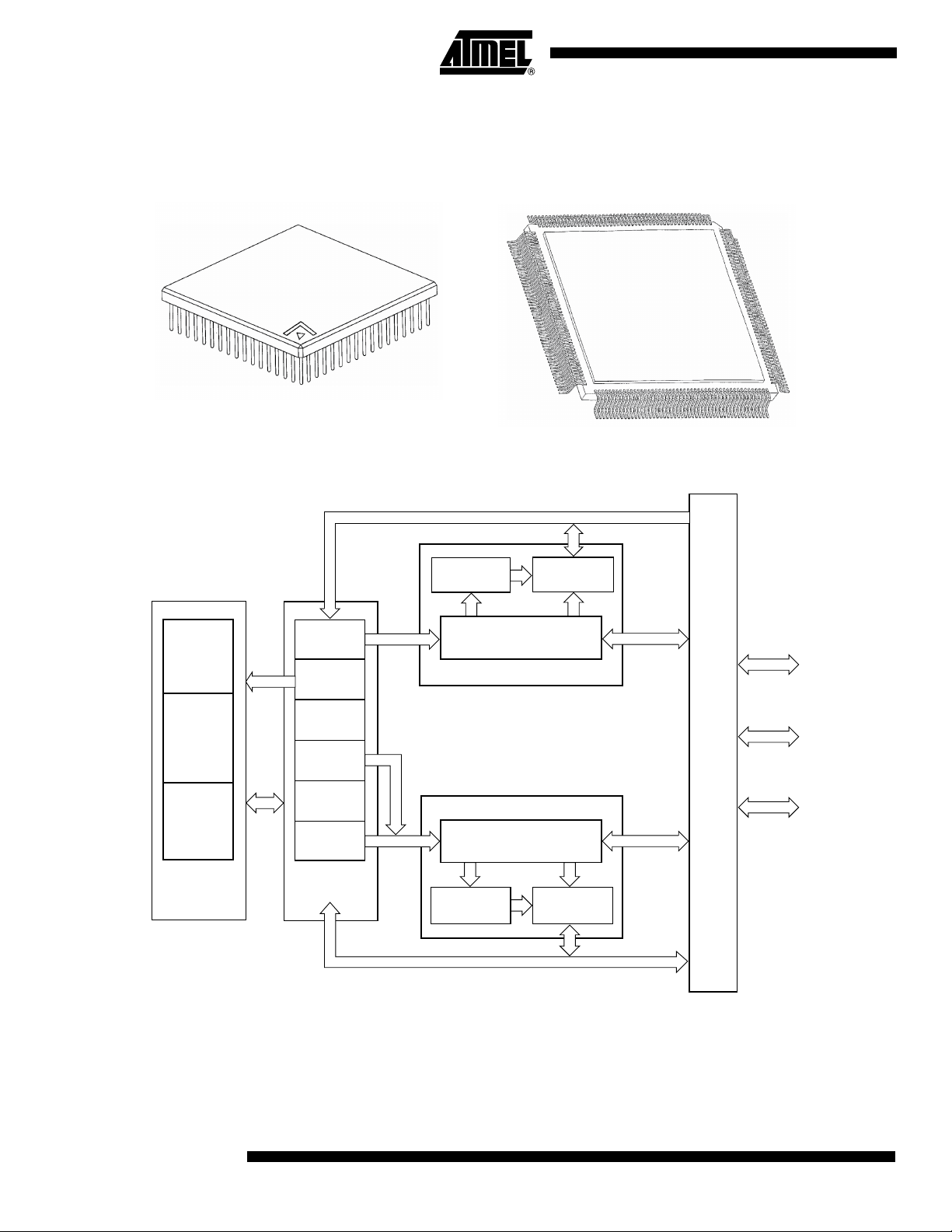
Figure 1. Block Diagram
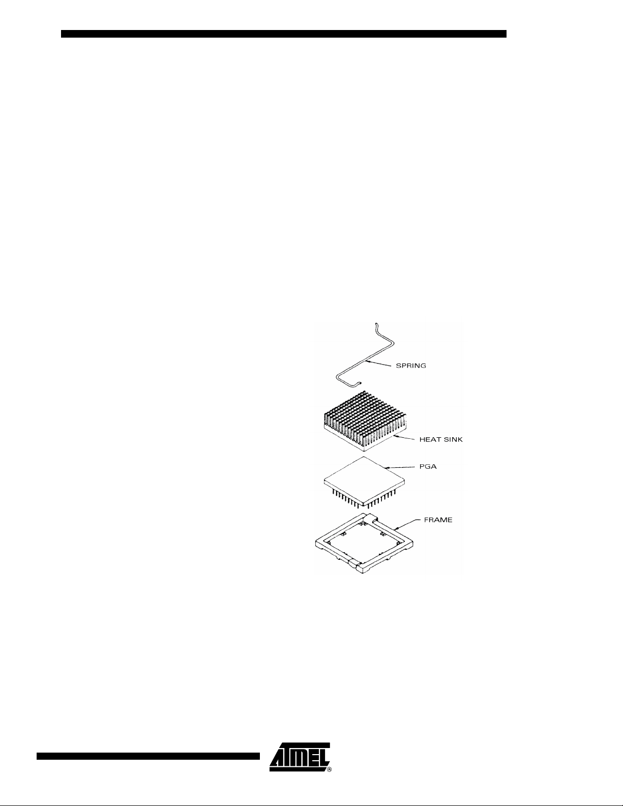
R suffix
PGA 179
Ceramic Pin Grid Array
Cavity Down
F suffix
CQFP 196
Gullwing Shape Lead
Ceramic Quad Fla Pack
INSTRUCTION DATA BUS
CONVERT
EXECUTE
WRITE
BACK
FLOATING-
POINT
UNIT
INSTRUCTION
FETCH
DECODE
EFFECTIVE
ADDRESS
CALCULATE
EFFECTIVE
ADDRESS
FETCH
EXECUTE
WRITE
BACK
INTEGER
UNIT
INSTRUCTION
ATC
INSTRUCTION
MMU/CACHE/SNOOP
CONTROLLER
INSTRUCTION
CACHE
INSTRUCTION MEMORY UNIT
DATA MEMORY UNIT
DATA
MMU/CACHE/SNOOP
CONTROLLER
DATA
ATC
OPERAND DATA BUS
DATA
CACHE
INSTRUCTION
ADDRESS
DATA
ADDRESS
B
U
S
C
O
N
T
R
O
L
L
E
R
ADDRESS
BUS
DATA
BUS
BUS
CONTROL
SIGNALS
2
TS68040
2116A–HIREL–09/02

TS68040
Introduction The TS68040 is an enhanced, 32-bit, HCMOS microprocessor that combines the inte-
ger unit processing capabilities of the TS68030 microprocessor with independent
4K bytes data and instruction caches and an on-chip FPU. The TS68040 maintains the
32-bit registers available with the entire TS68000 Family as well as the 32-bit address
and data paths, rich instruction set, and versatile addressing modes. Instruction execution proceeds in parallel with accesses to the internal caches, MMU operations, and bus
controller activity. Additionally, the integer unit is optimized for high-level language
environments.
The TS68040 FPU is user-object-code compatible with the TS68882 floating-point
coprocessor and conforms to the ANSI/IEEE Standard 754 for binary floating-point arithmetic. The FPU has been optimized to execute the most commonly used subset of the
TS68882 instruction set, and includes additional instruction formats for single and double-precision rounding of results. Floating-point instructions in the FPU execute
concurrently with integer instructions in the integer unit.
The MMUs support multiprocessing, virtual memory systems by translating logical
addresses to physical addresses using translation tables stored in memory. The MMUs
store recently used address mappings in two separate ATCs-on-chip. When an ATC
contains the physical address for a bus cycle requested by the processor, a translation
table search is avoided and the physical address is supplied immediately, incurring no
delay for address translation. Each MMU has two transparent translation registers available that define a one-to-one mapping for address space segments ranging in size from
16M bytes to 4G bytes each.
Each MMU provides read-only and supervisor-only protections on a page basis. Also,
processes can be given isolated address spaces by assigning each a unique table
structure and updating the root pointer upon a task swap. Isolated address spaces protect the integrity of independent processes.
The instruction and data caches operate independently from the rest of the machine,
storing information for fast access by the execution units. Each cache resides on its own
internal address bus and internal data bus, allowing simultaneous access to both. The
data cache provides write through or copyback write modes that can be configured on a
page-by-page basis.
The TS68040 bus controller supports a high-speed, non multiplexed, synchronous
external bus interface, which allows the following transfer sizes: byte, word (2 bytes),
long word (4 bytes), and line (16 bytes). Line accesses are performed using burst transfers for both reads and writes to provide high data transfer rates.
2116A–HIREL–09/02
3
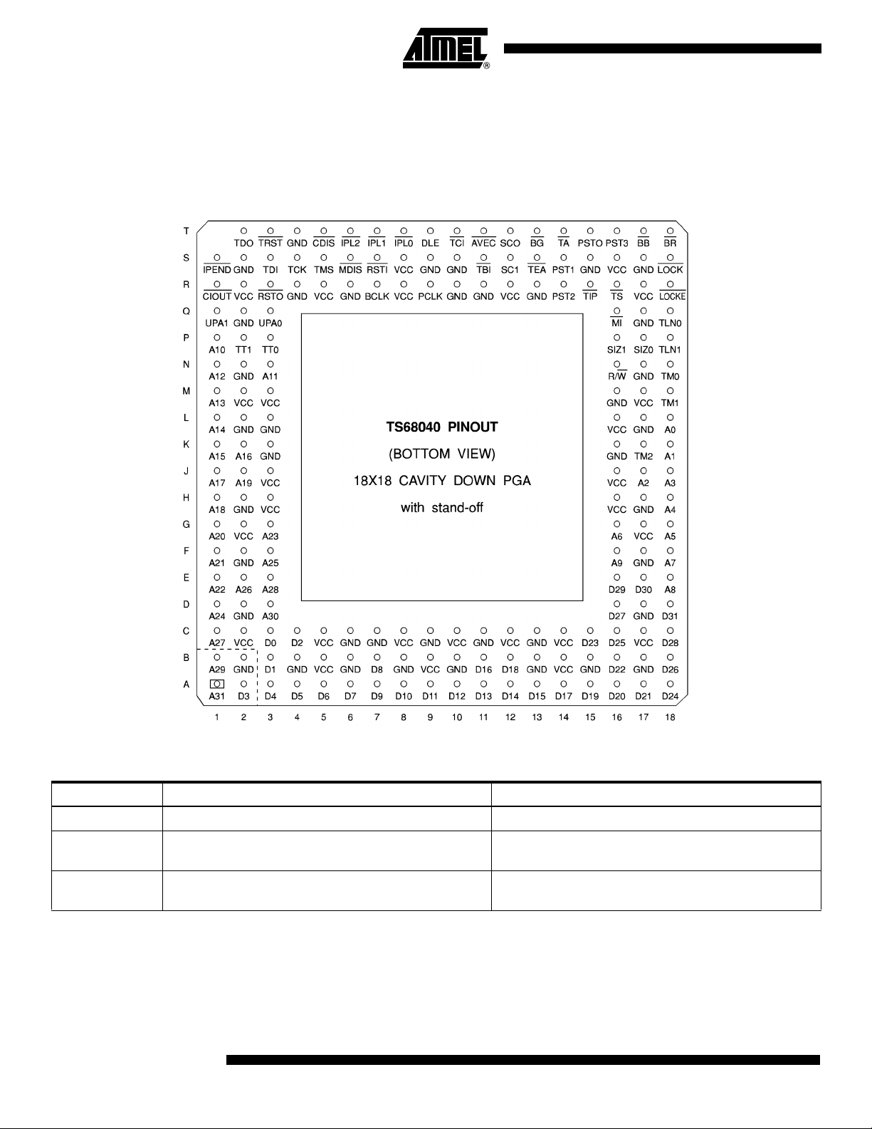
Pin Assignments
PGA 179
Figure 2. Bottom View
Table 1 . Power Supply Affectation to PGA Body
GND V
PLL S8
Internal Logic C6, C7, C9, C11,C13, K3, K16, L3, M16, R4, R11, R13,
S10,T4,S9,R6,R10
Output Drivers B2, B4, B6, B8, B10, B13, B15, B17, D2, D17, F2, F17,
H2, H17, L2, L17, N2, N17, Q2, Q17, S2, S15, S17
4
TS68040
CC
C5, C8, C10, C12, C14, H3, H16, J3, J16, L16, M3, R5,
R12, R8
B5, B9, B14, C2, C17, G2, G17, M2, M17, R2, R17,
S16
2116A–HIREL–09/02
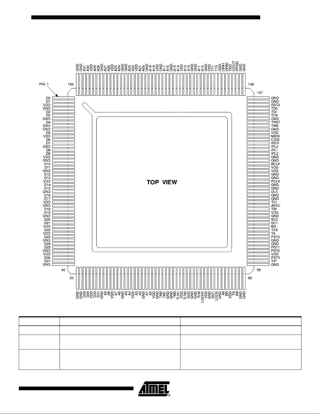
CQFP 196
Figure 3. Pin Assignments
TS68040
Table 2 . Power Supply Affectation to CQFP Body
GND V
PLL 127
Internal Logic 4, 9, 10, 19, 32, 45, 73, 88, 113, 119, 121, 122, 124,
125, 129, 130, 141, 159, 172
Output Drivers 7, 15, 22, 28, 35, 42, 49, 50, 51, 57, 63, 69, 76, 77, 83,
84, 91, 97, 98, 99, 105, 106, 146, 147, 148, 149, 155,
162, 163, 169, 176, 182, 183, 189, 195, 196
2116A–HIREL–09/02
CC
3, 18, 31, 40, 46, 60, 72, 87, 114, 126, 137, 158, 173,
186
12, 25, 38, 54, 66, 80, 94, 102, 152, 166, 179, 192
5
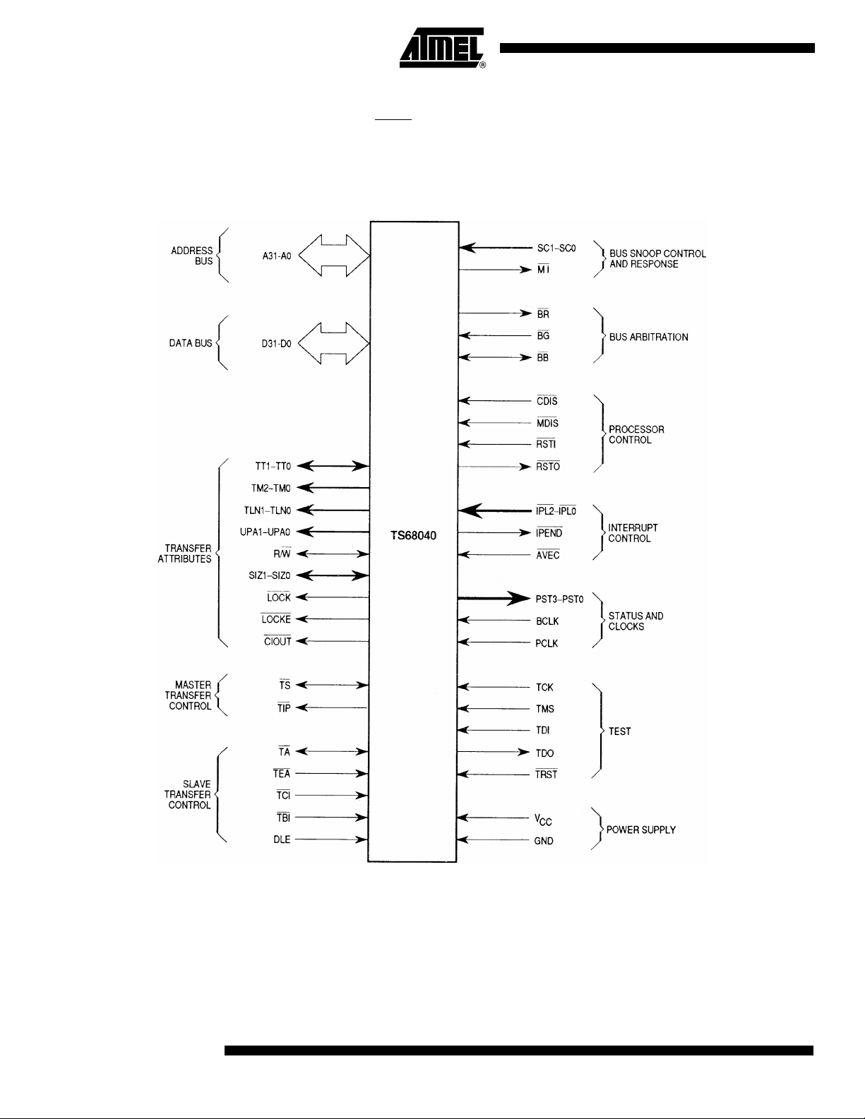
Signal Description Figure 4 and Table 3 describe the signals on the TS68040 and indicate signal functions.
The test signals, TRST
IEEE testability bus standard.
Figure 4. Functional Signal Groups
, TMS, TCK, TDI, and TDO, comply with subset P-1149.1 of the
6
TS68040
2116A–HIREL–09/02

Table 3 . Signal Index
Signal Name Mnemonic Function
Address Bus A31-A0 32-bit address bus used to address any of 4G bytes
Data Bus D31-D0 32-bit data bus used to transfer up to 32 bits of data per bus transfer
TS68040
Transfer Type TT1, TT0
Transfer Modifier TM2, TM0 Indicates supplemental information about the access
Transfer Line Number TLN1, TLN0
User Programmable Attributes
Read Write R/W
Transfer Size SIZ1, SIZ0
Bus Lock LOCK
BusLockEnd LOCKE
Cache Inhibit Out CIOUT
Transfer Start TS
Transfer in Progress TIP
Transfer Acknowledge TA
Transfer Error Acknowledge TEA
Transfer Cache Inhibit TCI
UPA1,
UPA0
Indicates the general transfer type: normal, MOVE 16, alternate logical function
code, and acknowledge
Indicates which cache line in a set is being pushed or loaded by the current line
transfer
User-defined signals, controlled by the corresponding user attribute bits from the
address translation entry
Identifies the transfer as a read or write
Indicates the data transfer size. These signals, together with A0 and A1, define the
active sections of the data bus
Indicates a bus transfer is part of a read-modify-write operation, and that the
sequence of transfers should not be interrupted
Indicates the current transfer is the last in a locked sequence of transfer
Indicates the processor will not cache the current bus transfer
Indicates the beginning of a bus transfer
Asserted for the duration of a bus transfer
Asserted to acknowledge a bus transfer
Indicates an error condition exists for a bus transfer
Indicates the current bus transfer should not be cached
Transfer Burst Inhibit TBI
Data Latch Enable DLE
Snoop Control SC1, SC0 Indicates the snooping operation required during an alternate master access
Memory Inhibit MI
Bus Request BR
Bus Grant BG
Bus Busy BB
Cache Disable CDIS
MMU Disable MDIS
Reset In RSTI
Reset Out RSTO
Interrupt Priority Level IPL2
Interrupt Pending IPEND
Autovector AVEC
Processor Status PST3-PST0 Indicates internal processor status
-IPL0 Provides an encoded interrupt level to the processor
Indicates the slave cannot handle a line burst access
Alternate clock input used to latch input data when the processor is operating in
DLE mode
Inhibits memory devices from responding to an alternate master access during
snooping operations
Asserted by the processor to request bus mastership
Asserted by an arbiter to grant bus mastership to the processor
Asserted by the current bus master to indicate it has assumed ownership of the bus
Dynamically disables the internal caches to assist emulator support
Disables the translation mechanism of the MMUs
Processor reset
Asserted during execution of the RESET instruction to reset external devices
Indicates an interrupt is pending
Used during an interrupt acknowledge transfer to request internal generation of the
vector number
2116A–HIREL–09/02
7

Table 3 . Signal Index (Continued)
Signal Name Mnemonic Function
Bus Clock BCLK Clock input used to derive all bus signal timing
Processor Clock PCLK
Test Clock TCK Clock signal for the IEEE P1149.1 test access port (TAP)
Test Mode Select TMS Selects the principle operations of the test-support circuitry
Test Data Input TDI Serial data input for the TAP
Test Data Output TDO Serial data output for the TAP
Test Reset TRST
Power Supply V
Ground GND Ground connection
CC
Clock input used for internal logic timing. The PCLK frequency is exactly 2X the
BCLK frequency
Provides an asynchronous reset of the TAP controller
Power supply
Scope This drawing describes the specific requirements for the microprocessor TS68040 -
25 MHz and 33 MHz, in compliance with MIL-STD-883 class B or Atmel standard
screening.
Applicable
Documents
MIL-STD-883 1. MIL-STD-883: test methods and procedures for electronics.
2. MIL-I-38535: general specifications for microcircuits.
3. DESC 5962-93143.
Requirements
General The microcircuits are in accordance with the applicable document and as specified
herein.
Design and Construction
Terminal Connections See Figure 2 and Figure 3.
Lead Material and Finish Lead material and finish shall be as specified in MIL-STD-883 (see enclosed “MIL-STD-
883 C and Internal Standard” on page 46).
Package The macro circuits are packaged in hermetically sealed ceramic packages which con-
form to case outlines of MIL-STD-1835-or as follow:
• CMGA 10-179-PAK pin grid array, but see “179 pins – PGA” on page 43.
• Similar to CQCC1-F196C-U6 ceramic uniform lead chip carrier package with
ceramic nonconductive tie-bar but use Atmel’s internal drawing, see “196 pins – Tie
Bar CQFP Cavity Up (on request)” on page 44.
• Gullwing shape CQFP see “196 pins – Gullwing CQFP cavity up” on page 45.
8
TS68040
2116A–HIREL–09/02
TS68040
The precise case outlines are described at the end of the specification (See “Package
Mechanical Data” on page 43.) and into MIL-STD-1835.
Electrical Characteristics
Absolute Maximum Ratings Stresses above the absolute maximum rating may cause permanent damage to the
device. Extended operation at the maximum levels may degrade performance and affect
reliability.
Table 4 . Absolute Maximum Ratings
Symbol Parameter Condition Min Max Unit
V
CC
V
I
Supply Voltage Range -0.3 7.0 V
Input Voltage Range -0.3 7.0 V
Large buffers enabled 7.7 W
P
D
T
C
T
stg
T
J
T
lead
Power Dissipation
Small buffers enabled 6.3 W
Operating Temperature -55 T
J
°C
Storage Temperature Range -65 +150 °C
Junction Temperature
(1)
+125 °C
Lead Temperature Max.10 sec soldering +300 °C
Note: 1. This device is not tested at TC = +125°C. Testing is performed by setting the junction temperature Tj = +125°C and allowing
the case and ambient temperatures to rise and fall as necessary so as not to exceed the maximum junction temperature.
Table 5 . Recommended Conditions of Use
Unless otherwise stated, all voltages are referenced to the reference terminal
Symbol Parameter Min Typ Max Unit
V
CC
V
IL
V
IH
V
OH
V
OL
f
c
T
C
T
J
Note: 1. This device is not tested at TC = +125°C. Testing is performed by setting the junction temperature T
the case and ambient temperatures to rise and fall as necessary so as not to exceed the maximum junction temperature.
Supply Voltage Range +4.75 +5.25 V
Logic Low Level Input Voltage Range GND
-0.3
0.8 V
Logic High Level Input Voltage Range +2.0 VCC+0.3 V
High Level Output Voltage 2.4 V
Low Level Output Voltage 0.5 V
Clock Frequency -25 MHz Version 25 MHz
-33 MHz Version 33 MHz
Case Operating Temperature Range
(1)
-55 T
Jmax
°C
Maximum Operating Junction Temperature +125 °C
=+125°C and allowing
J
2116A–HIREL–09/02
9

Thermal Considerations
General Thermal
Considerations
Thermal Device
Characteristics
Die and Package The TS68040 is being placed in a cavity-down alumina-ceramic 179-pin PGA that has a
This section is only given as user information.
As microprocessors are becoming more complex and requiring more power, the need to
efficiently cool the device becomes increasingly more important. In the past, the
TS68000 Family, has been able to provide a 0-70°C ambient temperature part for
speeds less than 40 MHz. However, the TS68040, which has a 50 MHz arithmetic logic
unit (ALU) speed, is specified with a maximum power dissipation for a particular mode, a
maximum junction temperature, and a thermal resistance from the die junction to the
case. This provides a more accurate method of evaluating the environment, taking into
consideration both the air-flow and ambient temperature available. This also allows a
user the information to design a cooling method which meets both thermal performance
requirements and constraints of the board environment.
This section discusses the device characteristics for thermal management, several
methods of thermal management, and an example of one method of cooling the
TS68040.
The TS68040 presents some inherent characteristics which should be considered when
evaluating a method of cooling the device. The following paragraphs discuss these
die/package and power considerations.
specified thermal resistance from junction to case of 1°C/W. This package differs from
previous TS68000 Family PGA packages which were cavity up. This cavity-down design
allows the die to be attached to the top surface of the package, which increases the ability of the part to dissipate heat through the package surface or an attached heat sink.
The maximum perimeter that the TS68040 allows for a heat sink on its surface without
interfering with the capacitor pads is 1.48" x 1.48". The specific dimensions and design
of the particular heat sink will need to be determined by the system designer considering
both thermal performance requirements and size requirements.
Power Considerations The TS68040 has a maximum power rating, which varies depending on the operating
frequency and the output buffer mode combination being used. The large buffer output
mode dissipates more power than the small, and the higher frequencies of operation
dissipate more power than the lower frequencies. The following paragraphs discuss
trade-offs in using the different output buffer modes, calculation of specific maximum
power dissipation for different modes, and the relationship of thermal resistances and
temperatures.
10
TS68040
2116A–HIREL–09/02
TS68040
Output Buffer Mode The 68040 is capable of resetting to enable for a combination of either large buffers or
small buffers on the outputs of the miscellaneous control signals, data bus, and address
bus/transfer attribute pins. The large buffers offer quicker output times, which allow for
an easier logic design. However, they do so by driving about 11 times as much current
as the small buffers (refer to TS68040 Electrical specifications for current output). The
designer should consider whether the quicker timings present enough advantage to justify the additional consideration to the individual signal terminations, the die power
consumption, and the required cooling for the device. Since the TS68040 can be powered-up in one of eight output buffer modes upon reset, the actual maximum power
consumption for TS68040 rated at a particular maximum operating frequency is dependent upon the power up mode. Therefore, the TS68040 is rated at a maximum power
dissipation for either the large buffers or small buffers at a particular frequency (refer to
TS68040 Electrical specifications). This allows the possibility of some of the thermal
management to be controlled upon reset. The following equation provides a rough
method to calculate the maximum power consumption for a chosen output buffer mode:
P
D=PDSB
+(P
DLB-PDSB
) · (PINSLB/PINS
)(1)
CLB
where:
P
D
= Max. power dissipation for output buffer mode
selected
P
DSB
= Max. power dissipation for small buffer mode
(all outputs)
P
DLB
= Max. power dissipation for large buffer mode
(all outputs)
PINS
PINS
= Number of pins large buffer mode
LB
= Number of pins capable of the large buffer
CLB
mode
Table 6 shows the simplified relationship on the maximum power dissipation for eight
possible configurations of output buffer modes.
Table 6 . Maximum Power Dissipation for Output Buffer Mode Configurations
Output Configuration Maximum Power Dissipation
Address Bus and
Data Bus
Transfer Attrib.
Small Buffer Small Buffer Small Buffer P
Small Buffer Small Buffer Large Buffer P
Small Buffer Large Buffer Small Buffer P
Small Buffer Large Buffer Large Buffer P
Large Buffer Small Buffer Small Buffer P
Large Buffer Small Buffer Large Buffer P
Large Buffer Large Buffer Small Buffer P
Large Buffer Large Buffer Large Buffer P
Misc. Control
Signals PD
+(P
DSB
+(P
DSB
+(P
DSB
+(P
DSB
+(P
DSB
+(P
DSB
+(P
DSB
DSB
DLB-PDSB
DLB-PDSB
DLB-PDSB
DLB-PDSB
DLB-PDSB
DLB-PDSB
DLB-PDSB
) · 13%
) · 52%
) · 65%
) · 35%
) · 48%
) · 87%
) · 100%
2116A–HIREL–09/02
11

To calculate the specific power dissipation of a specific design, the termination method
of each signal must be considered. For example, a signal output that is not connected
would not dissipate any additional power if it were configured in the large buffer rather
than the small buffer mode.
Relationships Between
Thermal Resistances and
Temperatures
Since the maximum operating junction temperature has been specified to be 125°C.
The maximum case temperature, TC, in °C can be obtained from:
T
C=TJ-PD
· Φ
JC
(2)
where:
= Maximum case temperature
T
C
= Maximum junction temperature
T
J
= Maximum power dissipation of the device
P
D
= Thermal resistance between the junction of the die and the case
Φ
JC
In general, the ambient temperature, T
T
A=TJ-PD
· ΦJC-PD· Φ
CA
Where the thermal resistance from case to ambient, Φ
,in°C is a function of the following formula:
A
(3)
, is the only user-dependent
CA
parameter once a buffer output configuration has been determined. As seen from equation (3), reducing the case to ambient thermal resistance increases the maximum
operating ambient temperature. Therefore, by utilizing such methods as heat sinks and
ambient air cooling to minimize the Φ
, a higher ambient operating temperature and/or
CA
a lower junction temperature can be achieved.
However, an easier approach to thermal evaluation uses the following formulas:
T
A=TJ-PD
· Φ
JA
(4)
or alternatively,
Thermal Management
Techniques
T
J=TA-PD
· Φ
JA
(5)
where:
= thermal resistance from the junction to the ambient (ΦJC+ ΦCA).
Φ
JA
This total thermal resistance of a package, Φ
Φ
and ΦCA. These components represent the barrier to heat flow from the semicon-
JC
ductor junction to the package (case) surface (Φ
ambient (Φ
). Although ΦJCis device related and cannot be influenced by the user, Φ
JC
, is a combination of its two components,
JA
) and from the case to the outside
JC
CA
is user dependent. Thus, good thermal management by the user can significantly
reduce Φ
achieving either a lower semiconductor junction temperature or a higher
CA
ambient operating temperature.
To attain a reasonable maximum ambient operating temperature, a user must reduce
the barrier to heat flow from the semiconductor junction to the outside ambient (Φ
The only way to accomplish this is to significantly reduce Φ
by applying such thermal
CA
JA
management techniques as heat sinks and ambient air cooling.
The following paragraphs discuss some results of a thermal study of the TS68040
device without using any thermal management techniques; using only air-flow cooling,
using only a heat sink, and using heat sink combined with air-flow cooling.
).
12
TS68040
2116A–HIREL–09/02
TS68040
Thermal Characteristics in
Still Air
A sample size of three TS68040 packages was tested in free-air cooling with no heat
sink. Measurements showed that the average Φ
was 22.8°C/W with a standard devia-
JA
tion of 0.44°C/W. The test was performed with 3W of power being dissipated from within
the package. The test determined that Φ
dissipation range possible. Therefore, since the variance in Φ
will decrease slightly for the increasing power
JA
within the possible
JA
power dissipation range is negligible, it can be assumed for calculation purposes that
Φ
is valid at all power levels. Using the formulas introduced previously, Table 7 shows
JA
the results of a maximum power dissipation of 3 and 5W with no heat sink or air-flow
(refer to Table 6 to calculate other power dissipation values).
Table 7 . Thermal Parameters With No Heat Sink or Air-flow
Defined Parameters Measured Calculated
P
D
T
J
Φ
JC
Φ
JA
ΦCA= ΦJA- Φ
JC
TC=TJ-PD* Φ
JC
TA=TJ-PD* Φ
3 Watts 125°C1°C/W 21.8°C/W 20.8°C/W 122°C 59.6°C
5 Watts 125°C1°C/W 21.8°C/W 20.8°C/W 120°C16°C
As seen by looking at the ambient temperature results, most users will want to implement some type of thermal management to obtain a more reasonable maximum
ambient temperature.
Thermal Characteristics in
Forced Air
A sample size of three TS68040 packages was tested in forced air cooling in a wind tunnel with no heat sink. This test was performed with 3W of power being dissipated from
within the package. As previously mentioned, since the variance in ΦJA within the possible power range is negligible, it can be assumed for calculation purposes that Φ
constant at all power levels. Using the previous formulas, Table 8 shows the results of
the maximum power dissipation at 3 and 5W with air-flow and no heat sink (refer to
Table 6 to calculate other power dissipation values).
JA
JA
is
Table 8 . Thermal Parameters With Forced Air Flow and No Heat Sink
Thermal Mgmt.
Technique Defined Parameters Measured Calculated
Air-flow velocity P
D
100 LFM 3W 125°C1°C/W 11.7°C/W 10.7°C/W 122°C 89.9°C
250 LFM 3W 125°C1°C/W 10°C/W 9°C/W 122°C95°C
500 LFM 3W 125°C1°C/W 8.9°C/W 7.9°C/W 122°C 98.3°C
750 LFM 3W 125°C1°C/W 8.5°C/W 7.5°C/W 122°C 99.5°C
1000 LFM 3W 125°C1°C/W 8.3°C/W 7.3°C/W 122°C 100.1°C
100 LFM 5W 125°C1°C/W 11.7°C/W 10.7°C/W 120°C 66.5°C
250 LFM 5W 125°C1°C/W 10°C/W 9°C/W, 120°C75°C
500 LFM 5W 125°C1°C/W 8.9°C/W 7.9°C/W 120°C 80.5°C
750 LFM 5W 125°C1°C/W 8.5°C/W 7.5°C/W 120°C 82.5°C
1000 LFM 5W 125°C1°C/W 8.3°C/W 7.3°C/W 120°C 83.5°C
T
J
Φ
JC
Φ
JA
Φ
CA
T
C
T
A
2116A–HIREL–09/02
13
By reviewing the maximum ambient operating temperatures, it can be seen that by
using the all-small-buffer configuration of the TS68040 with a relatively small amount of
air flow (100 LFM), a 0-70°C ambient operating temperature can be achieved. However,
depending on the output buffer configuration and available forced-air cooling, additional
thermal management techniques may be required.
Thermal Characteristics with
a Heat Sink
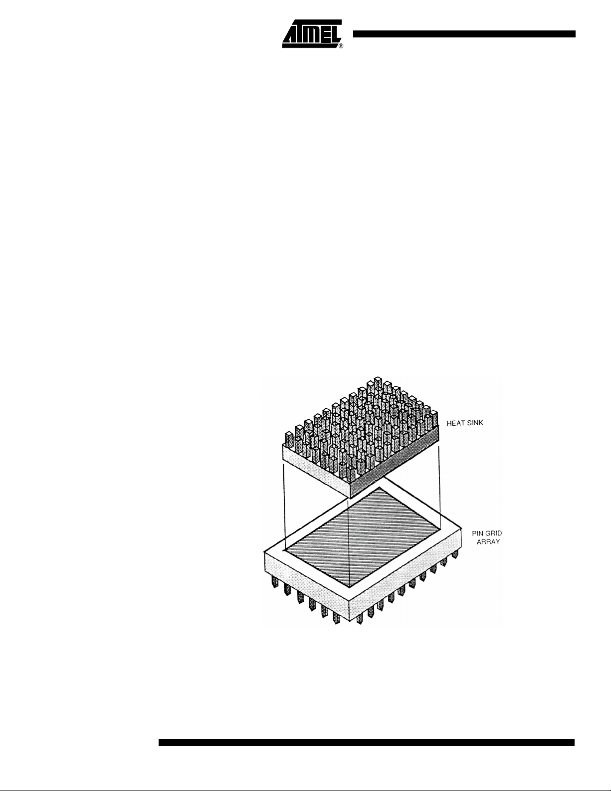
In choosing a heat sink the designer must consider many factors: heat sink size and
composition, method of attachment, and choice of a wet or dry connection. The following paragraphs discuss the relationship of these decisions to the thermal performance of
the design noticed during experimentation.
The heat sink size is one of the most significant parameters to consider in the selection
of a heat sink. Obviously a larger heat sink will provide better cooling. However, it is less
obvious that the most benefit of the larger heat sink of the pin fin type used in the experimentation would be at still air conditions. Under forced-air conditions as low as 100
LFM, the difference between the ΦCA becomes very small (0.4°C/W or less). This difference continues to decrease as the forced air flow increases. The particular heat sink
used in our testing fit the perimeter package surface area available within the capacitor
pads on the TS68040 (1.48" x 1.48") and showed a nice compromise between height
and thermal performance needs. The heat sink base perimeter area was 1.24" x 1.30"
and its height was 0.49". It was a pin-fin-type (i.e. bed of nails) design composed of Al
alloy. The heat sink is shown in Figure 5 can be obtained through Thermalloy Inc. by referencing part number 2338B.
Figure 5. Heat Sink Example
14
TS68040
2116A–HIREL–09/02
TS68040
All pin fin heat sinks tested were made from extrusion Al products. The planar face of
the heat sink mating to the package should have a good degree of planarity; if it has any
curvature, the curvature should be convex at the central region of the heat sink surface
to provide intimate physical contact to the PGA surface. All heat sinks tested met this
criteria. Nonplanar, concave curvature the central regions of the heat sink will result in
poor thermal contact to the package. A specification needs to be determined for the planarity of the surface as part of any heat sink design.
Although there are several ways to attach a heat sink to the package, it was easiest to
use a demountable heat sink attach called “E-Z attach for PGA packages” developed by
Thermalloy (see Figure 6). The heat sink is clamped to the package with the help of a
steel spring to a plastic frame (or plastic shoes Besides the height of the heat sink and
plastic frame, no additional height added to the package. The interface between the
ceramic package and the heat sink was evaluated for both dry and wet (i.e., thermal
grease) interfaces in still air. The thermal grease reduced the Φ
(about 2.5 °C/W) in still air. Therefore, it was used in all other testing done with the heat
sink. According to other testing, attachment with thermal grease provided about the
same thermal performance as if a thermal epoxy were used.
Figure 6. Heat Sink with Attachment
quite significantly
CA
2116A–HIREL–09/02
A sample size of one TS68040 package was tested in still air with the heat sink and
attachment method previously described. This test was performed with 3W of power
being dissipated from within the package. Since the variance in Φ
power range is negligible, it can be assumed for calculation purposes that Φ
within the possible
JA
JA
is constant at all power levels. Table 9 shows the result assuming a maximum power
dissipation of the part at 3 and 5W (refer to Table 6 to calculate other power dissipation
values).
15

Table 9 . Thermal Parameters With Heat Sink and No Air Flow
Thermal Mgmt.
Technique Defined Parameters Measured Calculated
Heat Sink P
D
T
J
Φ
JC
Φ
JA
Φ
CA
T
C
2338B 3W 125°C1°C/W 14°C/W 13°C/W 122°C83°C
2338B 5W 125°C1°C/W 14°C/W 13°C/W 120°C55°C
Thermal Characteristics with
a Heat Sink
and Forced Air
A sample size of three TS68040 packages was tested in forced-air cooling in a wind tunnel with a heat sink. This test was performed with 3W of power being dissipated from
within the package. As mentioned previously, the variance in Φ
power range is negligible; it can be assumed for calculation purposes that Φ
within the possible
JA
JA
all power levels. Table 10 shows the results, assuming a maximum power dissipation at
3 and 5W with air flow and heat sink thermal management (refer to Table 6 to calculate
other power dissipation values).
Table 1 0 . Thermal Parameters with Heat Sink and Air Flow
Thermal Mgmt. Technique Defined Parameters Measured Calculated
Air-flow Heat sink P
D
100 LFM 2338B 3W 125°C1°C/W 3.1°C/W 2.1°C/W 122°C 115.7°C
250 LFM 2338B 3W 125°C1°C/W 2.2°C/W 1.2°C/W 122°C 118.4°C
500 LFM 2338B 3W 125°C1°C/W 1.7°C/W 0.7°C/W 122°C 119.9°C
750 LFM 2338B 3W 125°C1°C/W 1.5°C/W 0.5°C/W 122°C 120.5°C
1000 LFM 2338B 3W 125°C1°C/W 1.4°C/W 0.4°C/W 122°C 120.8°C
T
J
Φ
JC
Φ
JA
Φ
CA
T
C
T
A
is valid at
T
A
100 LFM 2338B 5W 125°C1°C/W 3.1°C/W 2.1°C/W 120°C 109.5°C
250 LFM 2338B 5W 125°C1°C/W 2.2°C/W 1.2°C/W 120°C 114°C
500 LFM 2338B 5W 125°C1°C/W 1.7°C/W 0.7°C/W 120°C 116.5°C
750 LFM 2338B 5W 125°C1°C/W 1.5°C/W 0.5°C/W 120°C 117.5°C
1000 LFM 2338B 5W 125°C1°C/W 1.4°C/W 0.4°C/W 120°C 118°C
Thermal Testing Summary Testing proved that a heat sink in combination with a relatively small amount of air-flow
(100 LFM or less) will easily realize a 0-70°C ambient operating temperature for the
TS68040 with almost any configuration of the output buffers. A heat sink alone may be
capable of providing all necessary cooling, depending on the particular heat sink
height/size restraints, the maximum ambient operating temperature required, and the
output buffer configuration chosen. Also forced air cooling alone may attain a 0-70°C
ambient operating temperature. However this factor is highly dependent on the output
buffer configuration chosen and the available forced air for cooling. Figure 7 is a summary of the test results of the relationship between Φ
and air-flow for the TS68040.
JA
16
TS68040
2116A–HIREL–09/02

Figure 7. Relationship of ΦJAAir-Flow for PGA
TS68040
Table 1 1 . Characteristics Guaranteed
Package Symbol Parameter Value Unit
PGA 179
CQFP 196
Mechanical and
Environment
θ
J-A
θ
J-C
θ
J-A
θ
J-C
Thermal Resistance Junction-to-ambient See Figure 7 °C/W
Thermal Resistance Junction-to-case 1 °C/W
Thermal Resistance Junction-to-ambient TBD °C/W
Thermal Resistance Junction-to-case 1 °C/W
The microcircuits shall meet all mechanical environmental requirements of either MILSTD-883 for class B devices or for Atmel standard screening.
Marking The document where are defined the marking are identified in the related reference doc-
uments. Each microcircuit are legible and permanently marked with the following
information as minimum:
• Atmel Logo
• Manufacturer’s Part Number
• Class B Identification
• Date-code Of Inspection Lot
• ESD Identifier If Available
• Country Of Manufacturing
2116A–HIREL–09/02
17

Quality Conformance
Inspection
DESC/MIL-STD-883 Is in accordance with MIL-M-38535 and method 5005 of MIL-STD-883. Group A and B
inspections are performed on each production lot. Groups C and D inspection are performed on a periodical basis.
Electrical
Characteristics
General Requirements All static and dynamic electrical characteristics specified for inspection purposes and the
relevant measurement conditions are given below:
• Table 12: Static electrical characteristics for the electrical variants.
• Table 13: Dynamic electrical characteristics for TS68040 (25 MHz, 33 MHz).
For static characteristics (Table 12), test methods refer to IEC 748-2 method number,
where existing.
For dynamic characteristics (Table 13), test methods refer to clause “Static Characteristics” on page 18 of this specification.
Indication of “min.” or “max.” in the column «test temperature» means minimum or maximum operating temperature as defined in sub-clause Table 5 here above.
Static Characteristics
Table 1 2 . Electrical Characteristics
-55°C ≤ T
≤ T
C
Symbol Characteristic Min Max Unit
V
IH
V
IL
V
U
I
in
I
TSI
I
IL
I
IH
V
OH
; 4.75V ≤ VCC ≤ 5.25V unless otherwise specified
Jmax
Input High Voltage 2 V
Input Low Voltage GND 0.8 V
Undershoot -0.8 V
Input Leakage Current
at 0.5/2.4V
Hi-z (Off-state) Leakage Current
at 0.5/2.4V
Signal Low Input Current
V
=0.8V
IL
Signal High Input Current
V
=2.0V
IH
Output High Voltage
Larger Buffers - I
Small Buffers - I
OH
OH
=5mA
=35mA
IPLn
,MDIS, PCLK, RSTI,SCn,
An, BB,CIOUT, Dn, LOCK,
LOCKE
TIP
, TLNn, TMn, TS,TTn,UPAn
(1)(2)(3)(4)
AVEC,BCLKBG,CDIS,
TBI
,TCI,TCK,TEA
,R/W,SIZn,TA,TDO,
TMS, TDI, TRST
TMS, TDI, TRST
CC
-20 20 µA
-20 20 µA
-1.1 -0.18 mA
-0.94 -0.16 mA
2.4 V
V
18
TS68040
2116A–HIREL–09/02

TS68040
Table 1 2 . Electrical Characteristics (Continued)
-55°C ≤ T
≤ T
C
; 4.75V ≤ VCC ≤ 5.25V unless otherwise specified
Jmax
(1)(2)(3)(4)
Symbol Characteristic Min Max Unit
V
OL
P
D
C
in
Output Low Voltage
Larger buffers - I
Small buffers - I
OL
OL
=5mA
=35mA
Power Dissipation (TJ= 125°C)
Larger Buffers Enabled
Small Buffers Enabled
Capacitance - Note 4
V
=0V,f=1MHz
in
0.5 V
7.7
6.3
25 pF
Notes: 1. All testing to be performed using worst-case test conditions unless otherwise specified.
2. Maximum operating junction temperature (T
tested at T
= +125°. Testing is performed by setting the junction temperature TJ= +125°and allowing the case and ambient
C
) = +125°. Minimum case operating temperature (TC)=-55°.Thisdeviceisnot
J
temperatures to rise and fall as necessary so as not to exceed the maximum junction temperature.
3. Capacitance is periodically sampled rather than 100% tested.
4. Power dissipation may vary in between limits depending on the application.
Dynamic Characteristics
Table 1 3 . Clock AC Timing Specifications (see Figure 8)
-55°C ≤ T
≤ T
C
; 4.75V ≤ VCC ≤ 5.25V unless otherwise specified
Jmax
(1)(2)(3)(4)
25 MHz 33 MHz
W
Num Characteristic
Frequency of Operation 20 25 20 33 MHz
1PCLKCycleTime 20251525ns
(4)
(4)
(4)
(3)(4)
(3)(4)
1.7 1.7 ns
1.6 1.6 ns
47.5 52.5 46.67 53.33 %
9.5 10.5 7 8 ns
9.5 10.5 7 8 ns
2 PCLK Rise Time
3PCLKFallTime
4 PCLK Duty Cycle Measured at 1.5V
4a PCLK Pulse Width High Measured at 1.5V
4b PCLK Pulse Width Low Measured at 1.5V
5BCLKCycleTime 40503060ns
6, 7 BCLK Rise and Fall Time 4 3 ns
(4)
(4)
(4)
(4)
40 60 40 60 %
16 24 12 18 ns
16 24 12 18 ns
1000 1000 ppm
8 BCLK Duty Cycle Measured at 1.5V
8a BCLK Pulse Width High Measured at 1.5V
8b BCLK Pulse Width Low Measured at 1.5V
9 PCLK, BCLK Frequency Stability
10 PCLK to BCLK Skew 9 n/a ns
Notes: 1. All testing to be performed using worst-case test conditions unless otherwise specified.
2. Maximum operating junction temperature (T
tested at T
= +125°. Testing is performed by setting the junction temperature TJ= +125°and allowing the case and ambient
C
) = +125°. Minimum case operating temperature (TC)=-55°.Thisdeviceisnot
J
temperatures to rise and fall as necessary so as not to exceed the maximum junction temperature.
3. Specification value at maximum frequency of operation.
4. If not tested, shall be guaranteed to the limits specified.
UnitMin Max Min Max
2116A–HIREL–09/02
19
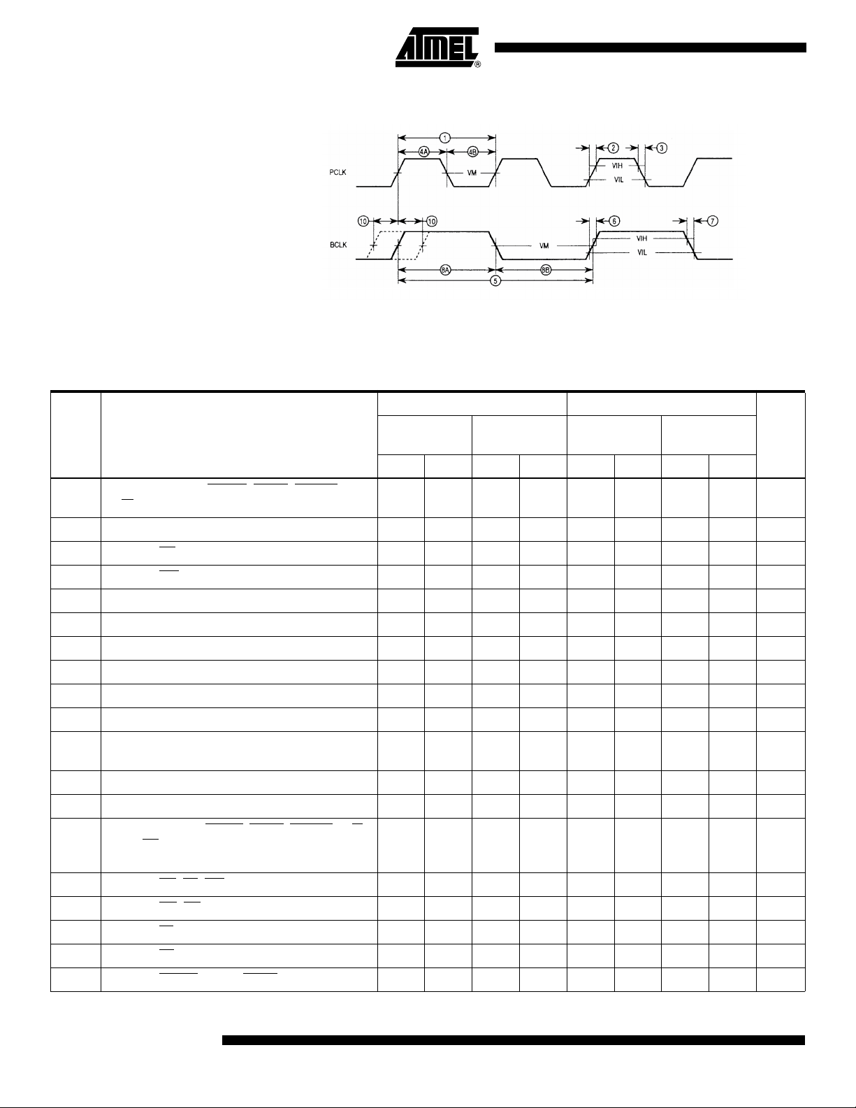
Figure 8. Clock Input Timing
Table 1 4 . Output AC Timing Specifications
(1)
(Figure 9 to Figure 15)
These output specifications are only for 25 MHz. They must be scaled for lower operating frequencies. Refer to
TS6804DH/AD for further information. -55°C ≤ T
≤ T
C
; 4.75V ≤ VCC ≤ 5.25V unless otherwise specified.
Jmax
25 MHz 33 MHz
Num Characteristic
11 BCLK to address CIOUT
R/W
, SIZn, TLN, TMn, UPAn valid
,LOCK,LOCKE,
(5)
Large
(1)
Buffer
Min Max Min Max Min Max Min Max
9 21 9 30 6.50 18 6.50 25 ns
Small
Buffer
(1)
Large
Buffer
(1)
12 BCLK to output invalid (output hold) 9 9 6.50 6.50 ns
13 BCLK to TS
14 BCLK to TIP
18 BCLK to data-out valid
19 BCLK to data-out invalid (output hold)
20 BCLK to output low impedance
valid 9 21 9 306.50186.5025 ns
valid 9 21 9 30 6.50 18 6.50 25 ns
(6)
(6)
(5)(6)
9 23 9 32 6.50 20 6.50 27 ns
9 9 6.50 6.50 ns
9 9 6.50 6.50 ns
21 BCLK to data-out high impedance 9 20 9 20 6.50 17 6.50 17 ns
26 BCLK to multiplexed address valid
27 BCLK to multiplexed address driven
(5)
(5)
19 31 19 40 14 26 14 33 ns
19 19 14 14 ns
(2)(3)(4)
Small
Buffer
(1)
Unit
28 BCLK to multiplexed address high
impedance
(5)(6)
29 BCLK to multiplexed data driven
30 BCLK to multiplexed data valid
38 BCLK to address CIOUT
SIZn, TS
impedance
39 BCLK to BB
40 BCLK to BR
43 BCLK to MI
48 BCLK to TA
50 BCLK to IPEND
20
TS68040
, TLNn, TMn, TTn, UPAn high
(5)
,TA,TIPhigh impedance 19 28 19 28 14 23 14 23 ns
,BBvalid 9 21 9 306.50186.5025 ns
valid 9 21 9 306.50186.5025 ns
valid 9 21 9 306.50186.5025 ns
, PSTn, RSTO valid 9 21 9 306.50186.5025 ns
,LOCK,LOCKE,R/W,
9 18 9 18 6.50 15 6.50 15 ns
(6)
(6)
19 19 14 20 14 20 ns
19 33 19 42 14 28 14 35 ns
9 18 9 18 6.50 15 6.50 15 ns
2116A–HIREL–09/02

TS68040
Notes: 1. Output timing is specified for a valid signal measured at the pin. Large buffer timing is specified driving a 50Ω transmission
line with a length characterized by a 2.5 ns one-way propagation delay, terminated through 50Ω to 2.5V. Large buffer output
impedance is typically 3Ω, resulting in incident wave switching for this environment. Small buffer timing is specified driving
an unterminated 30Ω transmission line with a length characterized by a 2.5 ns one-way propagation delay. Small buffer output impedance is typically 30Ω; the small buffer specifications include approximately 5 ns for the signal to propagate the
length of the transmission line and back.
2. All testing to be performed using worst-case test conditions unless otherwise specified.
3. The following pins are active low: AVEC
RST0
,RSTI,TA,TBI,TCI,TEA,TIP,TRST,TSand W of R/W.
4. Maximum operating junction temperature (T
tested at T
temperatures to rise and fall as necessary so as not to exceed the maximum junction temperature.
5. Timing specifications 11, 20 and 38 for address bus output timing apply when normal bus operation is selected. Specifications 26, 27 and 28 should be used when the multiplexed bus mode of operation is enabled.
6. Timing specifications 18 and 19 for data bus output timing apply when normal bus operation is selected. Specifications 28
and 29 should be used when the multiplexed bus mode of operation is enabled.
= +125°. Testing is performed by setting the junction temperature TJ= +125°and allowing the case and ambient
C
Table 1 5 . Input AC Timing Specifications (Figure 9 to Figure 15)
-55°C ≤ T
≤ T
C
; 4.75V ≤ VCC ≤ 5.25V unless otherwise specified
Jmax
,BG,BS,BR,CDIS,CIOUT, IPEND,IPLO,IPL1,IPL2,LOCK,LOCKE,MDIS,MI,
) = +125°. Minimum case operating temperature (TC)=-55°.Thisdeviceisnot
J
(1)(2)(3)(4)
25 MHz 33 MHz
Num Characteristic
15 Data-in Valid to BCLK (Setup) 5 4 ns
16 BCLK to Data-in Invalid (Hold) 4 4 ns
17 BCLK to Data-in High Impedance (Read Followed By Write) 49 36.5 ns
22a TA
22b TEA
22c TCI
22d TBI
23 BCLK to TA
24 AVEC
25 BCLK to AVEC
31 DLE Width High 8 8 ns
32 Data-in Valid to DLE (Setup) 2 2 ns
33 DLE to Data-in Invalid (Hold) 8 8 ns
34 BCLK to DLE Hold 3 3 ns
35 DLE High to BCLK 16 12 ns
36 Data-in Valid to BCLK (DLE Mode Setup) 5 5 ns
37 BCLK Data-in Invalid (DLE Mode Hold) 4 4 ns
ValidtoBCLK(Setup) 10 10 ns
Valid to BCLK (Setup) 10 10 ns
Valid to BCLK (Setup) 10 10 ns
Valid to BCLK (Setup) 11 10 ns
,TEA,TCI,TBIInvalid (Hold) 2 2 ns
ValidtoBCLK(Setup) 5 5 ns
Invalid (Hold) 2 2 ns
UnitMin. Max. Min. Max.
41a BB
41b BG
41c CDIS
41d IPLn
42 BCLK to BB
44a Address Valid to BCLK (Setup) 8 7 ns
44b SIZn Valid BCLK (Setup) 12 8 ns
2116A–HIREL–09/02
ValidtoBCLK(Setup) 7 7 ns
Valid to BCLK (Setup) 8 7 ns
,MDISValid to BCLK (Setup) 10 8 ns
ValidtoBCLK(Setup) 4 3 ns
,BG, CDIS,IPLn,MDISInvalid (Hold) 2 2 ns
21

Table 1 5 . Input AC Timing Specifications (Figure 9 to Figure 15) (Continued)
-55°C ≤ T
≤ T
C
; 4.75V ≤ VCC ≤ 5.25V unless otherwise specified
Jmax
(1)(2)(3)(4)
25 MHz 33 MHz
Num Characteristic
44c TTn Valid to BCLK (Setup) 6 8.5 ns
44d R/W
ValidtoBCLK(Setup) 6 5 ns
44e SCn Valid to BCLK (Setup) 10 11 ns
45 BCLK to Address SIZn, TTn, R/W
46 TS
47 BCLK to TS
49 BCLK to BB
51 RSTI
52 BCLK to RSTI
ValidtoBCLK(Setup) 5 9 ns
Invalid (Hold) 2 2 ns
High Impedance (68040 Assumes Bus Mastership) 9 9 ns
Valid to BCLK 5 4 ns
Invalid 2 2 ns
53 Mode Select Setup to RSTI
54 RSTI
Negated to Mode Selects Invalid
, SCn Invalid (Hold) 2 2 ns
Negated
(4)
(4)
20 20 ns
22ns
Notes: 1. All testing to be performed using worst-case test conditions unless otherwise specified.
2. The following pins are active low: AVEC
RST0
,RSTI,TA,TBI,TCI,TEA,TIP,TRST,TSand W of R/W.
3. Maximum operating junction temperature (T
tested at T
= +125°. Testing is performed by setting the junction temperature TJ= +125°and allowing the case and ambient
C
,BG,BS,BR,CDIS,CIOUT, IPEND,IPLO,IPL1,IPL2,LOCK,LOCKE,MDIS,MI,
) = +125°. Minimum case operating temperature (TC)=-55°.Thisdeviceisnot
J
temperatures to rise and fall as necessary so as not to exceed the maximum junction temperature.
4. The levels on CDIS
,MDIS,andtheIPL2-IPL0 signals enable or disable the multiplexed bus mode, data latch enable mode,
and driver impedance selection respectively.
UnitMin. Max. Min. Max.
22
TS68040
2116A–HIREL–09/02
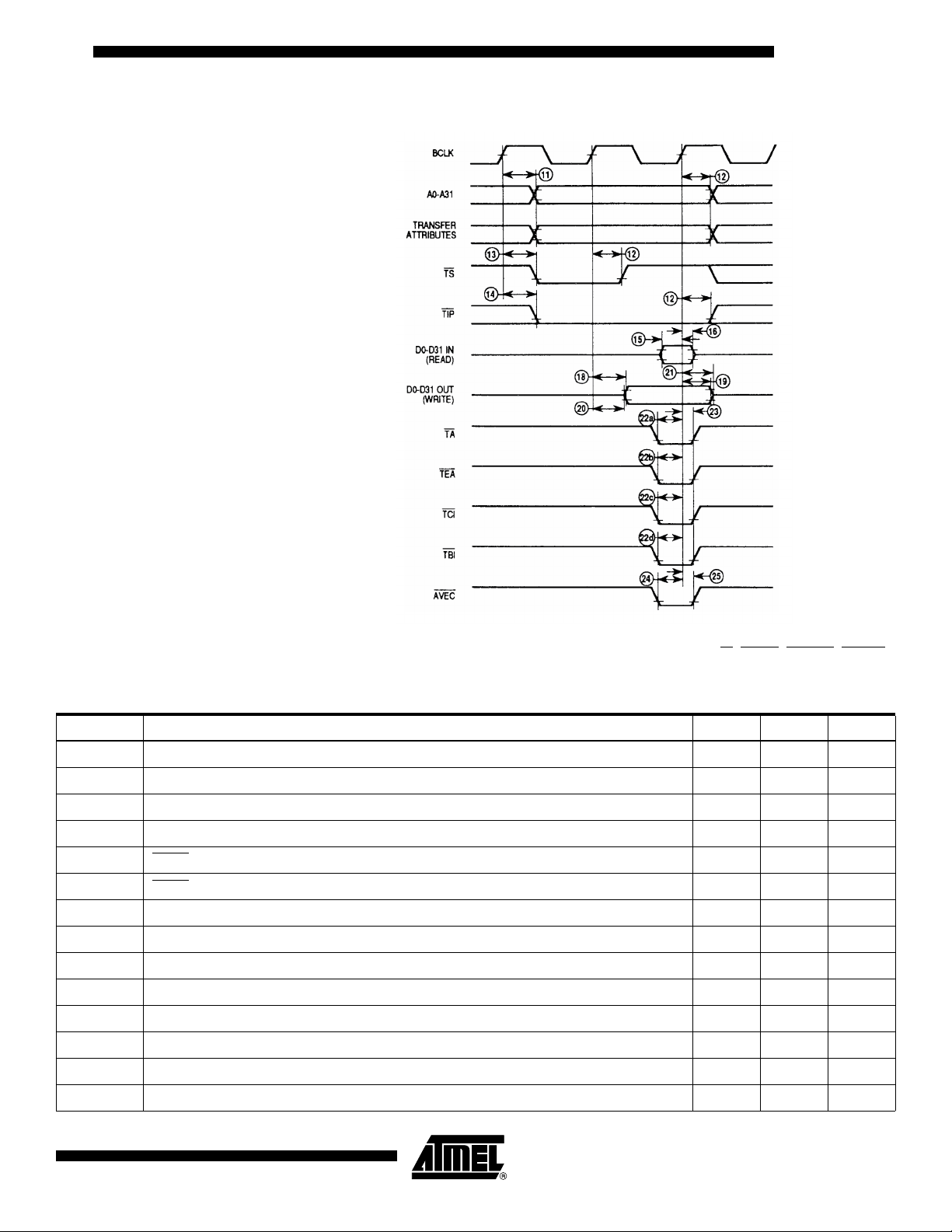
Figure 9. Read/Write Timing
TS68040
Note: Transfer attribute signals UPAN, SIZN, TTN, TMN, TLNN, R/W,LOCK,LOCKE,CIOUT
Table 1 6 . JTAG Timing Application (Figure 16 to Figure 19)
-55°C ≤ T
Num Characteristic Min Max Unit
≤ TJmax; 4.75V ≤ VCC ≤ 5.25V unless otherwise specified
C
TCK Frequency 010MHz
1 TCK Cycle Time 100 ns
2 TCK Clock Pulse Width Measured at 1.5V 40 ns
3 TCK Rise and Fall Times 0 10 ns
4TRST
5TRST
6 Boundary Scan Input Data Setup Time 50 ns
7 Boundary Scan Input Data Hold Time 50 ns
8 TCK to Output Data Valid 0 50 ns
9 TCK to Output High Impedance 0 50 ns
10 TMS, TDI Data Setup Time 20 ns
11 TMS, TDI Data Hold Time 5 ns
12 TCK to TDO Data Valid 0 20 ns
13 TCK to TDO High Impedance 0 20 ns
SetupTimetoTCKFallingEdge 40 ns
Assert Time 100 ns
(1)(2)
2116A–HIREL–09/02
23

Notes: 1. All testing to be performed using worst-case test conditions unless otherwise specified.
2. Maximum operating junction temperature (T
tested at T
temperatures to rise and fall as necessary so as not to exceed the maximum junction temperature.
= +125°. Testing is performed by setting the junction temperature TJ= +125° and allowing the case and ambient
C
) = +125°. Minimum case operating temperature (TC)=-55°.Thisdeviceisnot
J
Table 1 7 . Boundary Scan Instruction Codes
Bit 2 Bit 1 Bit 0 Instruction Selected Test Data Register Accessed
0 0 0 Extest Boundary Scan
0 0 1 Highz Bypass
0 1 0 Sample/Preload Boundary Scan
0 1 1 DRVCTLT Boundary Scan
1 0 0 Shutdown Bypass
1 0 1 Private Bypass
1 1 0 DRVCTLS Boundary Scan
1 1 1 Bypass Bypass
Switching Test Circuit
and Waveforms
Figure 10. Address and Data Bus Timing — Multiplexed Bus Mode
24
TS68040
2116A–HIREL–09/02

Figure 11. DLE Timing Burst Access
Figure 12. Bus Arbitration Timing
TS68040
2116A–HIREL–09/02
25
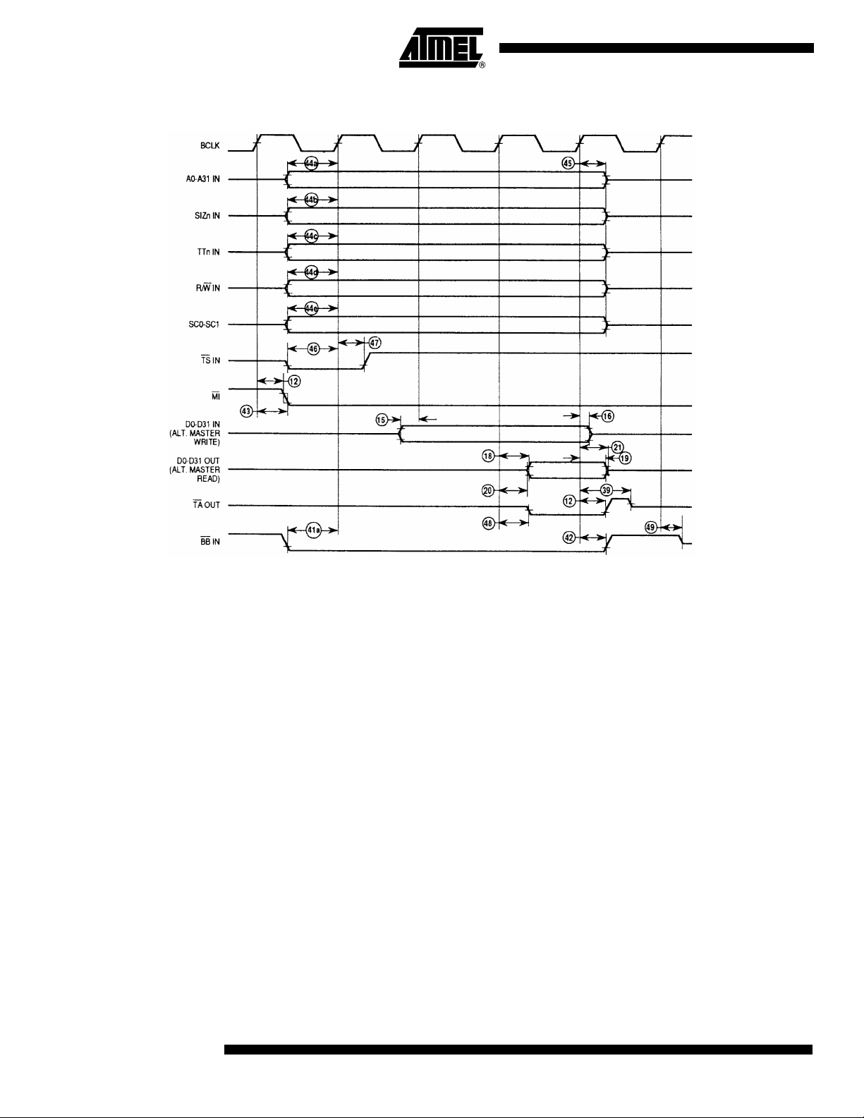
Figure 13. Snoop Hit Timing
26
TS68040
2116A–HIREL–09/02

Figure 14. Snoop Miss Timing
TS68040
Figure 15. Other Signal Timing
2116A–HIREL–09/02
27

Figure 16. Clock Input Timing Diagram
Figure 17. TRST
Figure 18. Boundary Scan Timing Diagram
Timing Diagram
28
TS68040
2116A–HIREL–09/02

Functional
TS68040
Figure 19. Test Access Port Timing Diagram
Description
Programming Model The TS68040 integrates the functions of the integer unit, MMU, and FPU. As shown in
Figure 20, the registers depicted in the programming model provide access and control
for the three units. The registers are partitioned into two levels of privilege: user and
supervisor. User programs, executing in the user mode, can only use the resources of
the user model. System software, executing in the supervisor mode, has unrestricted
access to all processor resources.
The integer portion of the user programming model, consisting of 16, general-purpose,
32-bit registers and two control registers, is the same as the user programming model of
the TS68030. The TS68040 user programming model also incorporates the TS68882
programming model consisting of eight, floating-point, 80-bit data registers, a floatingpoint control register, a floating-point status register, and a floating-point instruction
address register.
The supervisor programming model is used exclusively by TS68040 system programmers to implement operating system functions, I/O control, and memory management
subsystems. This supervisor/user distinction in the TS68000 architecture was carefully
planned so that all application software can be written to execute in the nonprivileged
user mode and migrate to the TS68040 from any TS68000 platform without modification. Since system software is usually modified by system designers when porting to a
new design, the control features are properly placed in the supervisor programming
model. For example, the transparent translation registers of the TS68040 can only be
read or written by the supervisor software; the programming resources of user application programs are unaffected by the existence of the transparent translation registers
2116A–HIREL–09/02
Registers D0-D7 are data registers containing operands for bit and bit field (1- to 32-bit),
byte (8-bit), word (16-bit), long-word (32-bit), and quad-word (64-bit) operations. Registers A0-A6 and the stack pointer registers (user, interrupt, and master) are address
registers that may be used as software stack pointers or base address registers. Register A7 is the user stack pointer in user mode, and is either the interrupt or master stack
pointer (A7’ or A7’’) in supervisor mode. In supervisor mode, the active stack pointer
(interrupt or master) is selected based on a bit in the status register (SR). The address
29

registers may be used for word and long-word operations, and all of the 16 general-purpose registers (D0-D7, A0-A7 in Figure 20) may be used as index registers.
The eight, 80-bit, floating-point data registers (FP0-FP7) are analogous to the integer
data registers (D0-D7) of all TS68000 Family processors. Floating-point data registers
always contain extended-precision numbers. All external operands, regardless of the
data format, are converted to extended-precision values before being used in any floating-point calculation or stored in a floating-point data register.
The program counter (PC) usually contains the address of the instruction being executed by the TS68040. During instruction execution and exception processing, the
processor automatically increments the contents of the PC or places a new value in the
PC, as appropriate. The status register (SR in the supervisor programming model) contains the condition codes that reflect the results of a previous operation and can be used
for conditional instruction execution in a program. The lower byte of the SR is accessible
in user mode as the condition code register (CCR). Access to the upper byte of the SR
is restricted to the supervisor mode.
As part of exception processing, the vector number of the exception provides an index
into the exception vector table. The base address of the exception vector table is stored
in the vector base register (VBR). The displacement of an exception vector is added to
the value in the VBR when the TS68040 accesses the vector table during exception
processing.
Alternate function code registers, SFC and DFC (source and destination), contain 3-bit
function codes. Function codes can be considered extensions of the 32-bit linear
address. Function codes are automatically generated by the processor to select address
spaces for data and program accesses at the user and supervisor modes. The alternate
function code registers are used by certain instructions to explicitly specify the function
codes for various operations. The cache control register (CACR) controls enabling of
the on-chip instruction and data caches of the TS68040.
The supervisor root pointer (SRP) and user root pointer (URP) registers point to the root
of the address translation table tree to be used for supervisor mode and user mode
accesses. The URP is used if FC2 of the logical address is zero, and the SRP is used if
FC2 is one.
The translation control register (TC) enables logical-to-physical address translation and
selects either 4K or 8K page sizes. As shown in Figure 20, there are four transparent
translation registers - ITT0 and ITT1 for instruction accesses and DTT0 and DTT1 for
data accesses. These registers allow portions of the logical address space to be transparently mapped and accessed without the use of resident descriptors in an ATC. The
MMU status register (MMUSR) contains status information from the execution of a
PTEST instruction. The PTEST instruction searches the translation tables for the logical
address as specified by this instruction’s effective address field and the DFC.
The 32-bit floating-point control register (FPCR) contains an exception enable byte that
enables disables traps for each class of floating-point exceptions and a mode byte that
sets the user-selectable modes. The FPCR can be read or written to by the user and is
cleared by a hardware reset or a restore operation of the null state. When cleared, the
FPCR provides the IEEE 754 standard defaults. The floating-point status register
(FPSR) contains a condition code byte, quotient bits, an exception status byte, and an
accrued exception byte. All bits in the FPSR can be read or written by the user. Execution of most floating-point instructions modifies this register.
30
TS68040
2116A–HIREL–09/02

TS68040
For the subset of the FPU instructions that generate exception traps, the 32-bit floatingpoint instruction address register (FPIAR) is loaded with the logical address of an
instruction before the instruction is executed. This address can then be used by a floating-point exception handler to locate a floating-point instruction that has caused an
exception. The move floating-point data register (FMOVE) instruction (to from the
FPCR, FPSR, or FPIAR) and the move multiple data registers (FMOVEN) instruction
cannot generate floating-point exceptions; therefore, these instructions do not modify
theFPIAR.Thus,theFMOVEandFMOVEMinstructionscanbeusedtoreadthe
FPIAR in the trap handler without changing the previous value.
Figure 20. Programming Model
2116A–HIREL–09/02
31

Data Types and
Addressing Modes
The TS68040 supports the basic data types shown in Table 18. Some data types apply
only to the integer unit, some only to the FPU, and some to both the integer unit and the
FPU. In addition, the instruction set supports operations on other data types such as
memory addresses.
Table 1 8 . Data Types
Operand Data Type Size Execution Unit (IU
Bit 1-bit IU
Bit Field 1-32 bits IU Field of consecutive bits
(1)
,FPU) Notes
BCD 32 bits
Byte Integer 8 bits IU, FPU
Word Integer 16 bits IU, FPU
Long-word Integer 32 bits IU, FPU
Quad-word Integer 64 bits IU Any two data registers
16-byte 128 bits IU Memory-only, aligned 16-byte boundary
Single-precision Real 32 bits FPU 1-bit sign, 8-bit exponent, 23-bit mantissa
Double-precision Real 64 bits FPU 1-bit sign, 11-bit exponent, 52-bit mantissa
Extended-precision Real 80 bits FPU 1-bit sign, 15-bit exponent, 64-bit mantissa
Note: 1. IU = Integer Unit.
IU Packaged: 2 digits byte
Unpacked: 1 digit byte
The three integer data formats that are common to both the integer unit and the FPU
(byte, word, and long word) are the standard twos-complement data formats defined in
the TS68000 Family architecture. Whenever an integer is used in a floating-point operation, the integer is automatically converted by the FPU to an extended-precision floatingpoint number before being used. The ability to effectively use integers in floating-point
operations saves user memory because an integer representation of a number usually
requires fewer bits than the equivalent floating-point representation.
Single- and double-precision floating-point data formats are implemented in the FPU as
defined by the IEEE standard. These data formats are the main floating-point formats
and should be used for most calculations involving real numbers.
32
The extended-precision data format is also in conformance with the IEEE standard, but
the standard does not specify this format to the bit level as it does for single- and double-precision. The memory format for the FPU consists of 96 bits (three long words).
Only 80 bits are actually used; the other 16 bits are reserved for future use and for longword alignment of the floating-point data structures in memory. The extended-precision
format has a 15-bit exponent, a 64-bit mantissa, and a 1-bit mantissa sign. Extendedprecision numbers are intended for use as temporary variables, intermediate values, or
where extra precision is needed.
The TS68040 addressing modes are shown in Table 19. The register indirect addressing modes support post-increment, predecrement, offset, and indexing, which are
particularly useful for handling data structures common to sophisticated applications
and high-level languages. The program counter indirect mode also has indexing and offset capabilities; this addressing mode is typically required to support positionindependent software. In addition to these addressing modes, the TS68040 provides
index sizing and scaling features that enhance software performance. Data formats are
supported orthogonally by all arithmetic operations and by all appropriate addressing
modes.
TS68040
2116A–HIREL–09/02

Table 1 9 . Addressing Modes
Addressing Modes Syntax
Register Direct
Date Register Direct
Address Register Direct
Register Indirect
Address Register Indirect
Address Register Indirect With Postincrement
Address Register Indirect With Predecrement
Address Register Indirect With Displacement
Register Indirect With Index
Address Register Indirect With Index (8-bit Displacement)
Address Register Indirect With Index (Base Displacement)
Memory Indirect
Memory Indirect Postincrement
Memory Indirect Preindexed
Program Counter Indirect With Displacement (d
Program Counter Indirect With Index
PC Indirect With Index (8-bit Displacement)
PC Indirect With Index (Base Displacement
Program Counter Memory Indirect
PC Memory Indirect Postindexed
PC Memory Indirect Preindexed
Dn
An
(An)
(An)
(An)
(d
16
,An,Xn)
(d
8
(bd, An, Xn)
([bd, An], Xn, od)
([bd, An, Xn], od)
16
,PC,Xn)
(d
8
(bd, PC, Xn)
([bd, PC], Xn, od)
([bd, PC, Xn], od)
TS68040
,An)
,PC)
Absolute
Absolute Short
Absolute Long
Immediate # (data)
Note:
xxx.W
xxx.L
DN = Data register, D0-D7
AN = Address register, A0-A7
d
= A twos-complement or sign-extended displacement; added as part of the effective address calculation;
8,d16
size is 8 (d
)or16(d16) bits; when omitted, assemblers use a value of zero.
8
Xn = Address or data register used as an index register; form is Xn, SIZE*SCALE, where SIZE is W or L
(indicates index register size) and SCALE is 1, 2, 4 or 8 (index register os multiplied by SCALE); use of
SIZE and or SCALE is optional.
bd = A twos-complement base displacement; when present, size can be 16 or 32 bits.
od = Outer displacement added as part of effective address calculation after any memory indirection; use is
optionalwithasizeof16or32bits.
PC = Program counter.
(data) = Immediate value of 8, 16 or 32 bits.
( ) = Effective address.
[ ] = Used as indirect address to long-word address.
– Instruction Set Overview
2116A–HIREL–09/02
33

The instruction provided by the TS68040 are listed in Table 20. The instruction set has
been tailored to support high-level languages and is optimized for those instructions
most commonly executed (however, all instructions listed are fully supported). Many
instructions operate on bytes, words, and long words, and most instructions can use any
of the addressing modes of Table 19.
Table 20. Instruction Set Summary
Mnemonic Description
ABCD
ADD
ADDA
ADDI
ADDQ
ADDX
AND
ANDI
ASL, ASR
Bcc
BCHG
BCLR
BFCHG
BFCLR
BFEXTS
BFEXTU
BFFFO
BFINS
BFSET
BFTST
BKPT
BRA
BSET
BSR
BTST
CAS
CAS2
CHK
CHK2
(1)
CINV
CLR
CMP
CMPA
CMPI
CMPM
CMP2
CPUSH
(1)
Add Decimal With Extend
Add
Add Address
Add Immediate
Add Quick
AddWithExtend
Logical AND
Logical AND Immediate
Arithmetic Shift Left And Right
Branch Conditionally
Test Bit And Change
Te st B it A nd C lea r
Test Bit Field And Change
Test Bit Field And Clear
Signed Bit Field Extract
Unsigned Bit Field Extract
Bit Field Find First One
Bit Field Insert
Test Bit Field And Set
Te st B it F ie ld
Breakpoint
Branch
Test Bit And Set
Branch To Subroutine
Te st B it
Compare And Swap Operands
Compare And Swap Dual Operands
Check Register Against Bounds
Check Register Against Upper And Lower Bounds
Invalidate Cache Entries
Clear
Compare
Compare Address
Compare Immediate
Compare Memory To Memory
Compare Register Against Upper And Lower Bounds
Push Then Invalidate Cache Entries
34
TS68040
DB
CC
DIVS, DIVSL
DIVU, DIVUL
EOR
EORI
EXG
EXT, EXTB
Test Condition, Decrement And Branch
Signed Divide
Unsigned Divide
Logical Exclusive OR
Logical Exclusive OR Immediate
Exchange Registers
Sign Extend
2116A–HIREL–09/02

Table 20. Instruction Set Summary (Continued)
Mnemonic Description
ILLEGAL Take Illegal Instruction Trap
TS68040
JMP
JSR
LEA
LINK
LSL, LSR
MOVE
MOVE16
(1)
MOVEA
MOVE CCR
MOVE SR
MOVE USP
MOVEC
(1)
MOVEM
MOVEP
MOVEQ
MOVES
(1)
MULS
MULU
NBCD
NEG
NEGX
NOP
NOT
OR
ORI
Jump
Jump To Subroutine
Load Effective Address
Link And Allocate
Logical Shift Left And Right
Move
16-byte Block Move
Move Address
Move Condition Code Register
Move Status Register
Move User Stack Pointer
Move Control Register
Move Peripheral
Move Quick
Move Alternate Address Space
Move Multiply
Signed Multiply
Unsigned Multiply
Negate decimal with extend
Negate
Negate with extend
No operation
Logical complement
Logical Inclusive OR
Logical Inclusive OR Immediate
PAC K
PEA
PFLUSH
PTEST
(1)
(1)
RESET
ROL, ROR
ROXL, ROXR
RTD
RTE
RTR
RTS
Pack BCD
Push Effective Address
Flush Entry(ies) In The ATCs
Test A Logical Address
Reset External Devices
Rotate Left And Right
Rotate With Extend Left And Right
Return And Deallocate
Return From Exception
Return And Restore Codes
Return From Subroutine
2116A–HIREL–09/02
35

Table 20. Instruction Set Summary (Continued)
Mnemonic Description
SBCD
Scc
STOP
SUB
SUBA
SUBI
SUBQ
SUBX
SWAP
TA S
TRAP
TRAPcc
TRAPV
TST
UNLK
UNPK
Substract Decimal With Extend
Set Conditionally
Stop
Subtract
Subtract Address
Subtract Immediate
Subtract Quick
Subtract With Extend
Swap Register Words
Test Operand And Set
Tra p
Trap Conditionally
Trap On Overflow
Trap Operand
Unlink
Unpack BCD
Note: 1. TS6840 additions or alterations to the TS68030 and TS68881/TS68882 instructions
sets.
Table 21. Floating-point instructions
Mnemonic Description
(1)
FABS
(1)
FADD
FBcc
FCMP
FDBcc
(1)
FDIV
FMOVE
FMOVEM
FMUL
FNEG
(1)
(1)
(1)
FRESTORE
FSAVE
FScc
(1)
FSQRT
(1)
FSUB
FTRAPcc
FTST
Note: 1. TS6840 additions or alterations to the TS68030 and TS68881/TS68882 instructions
sets.
Floating-point Absolute Value
Floating-point Add
Branch On Floating-point Condition
Floating-point Compare
Floating-point Decrement And Branch
Floating-point Divide
Move Floating-point Register
Move Multiple Floating-point Registers
Floating-point Multiply
Floating-point Negate
Restore Floating-point Internal State
Save Floating-point Internal State
Set According To Floating-point Condition
Floating-point Square Root
Floating-point Substract
Trap On Floating-point Condition
Floating-point Test
36
The TS68040 floating-point instructions, a commonly used subset of the TS68882
instruction set, are implemented in hardware. The remaining unimplemented instructions are less frequently used and are efficiently emulated in software, maintaining
compatibility with the TS68881/TS68882 floating-point coprocessors.
The TS68040 instruction set includes MOVE16, a new user instruction that allows highspeed transfers of 16-byte blocks between external devices such as memory to memory
or coprocessor to memory.
TS68040
2116A–HIREL–09/02

TS68040
Instruction and Data
Caches
Cache Organization The instruction and data caches are four-way set-associative with 64 sets of four, 16-
Studies have shown that typical programs spend much of their execution time in a few
main routines or tight loops. Earlier members of the TS68000 Family took advantage of
this locality of reference phenomenon to varying degrees. The TS68040 takes further
advantage of cache technology with its two, independent, on-chip, physical address
space caches, one for instructions and one for data. The caches reduce the processor’s
external bus activity and increase CPU throughput by lowering the effective memory
access time. For a typical system design, the large caches of the TS68040 yield a very
high hit rate, providing a substantial increase in system performance. Additionally, the
caches are automatically burstfilled from the external bus whenever a cache miss
occurs.
The autonomous nature of the caches allows instruction-stream fetches, data-stream
fetches, and a third external access to occur simultaneously with instruction execution.
For example, if the TS68040 requires both an instruction-stream access and an external
peripheral access and if the instruction is resident in the on-chip cache, the peripheral
access proceeds unimpeded rather than being queued behind the instruction fetch. If a
data operand is also required and if it is resident in the data cache, it can also be
accessed without hindering either the instruction access from its cache or the peripheral
access external to the chip. The parallelism inherent in the TS68040 also allows multiple
instructions that do not require any external accesses to execute concurrently while the
processor is performing an external access for a previous instruction.
byte lines for a total cache storage of 4K bytes each. As shown in Figure 21, each 16byte line contains an address tag and state information. State information for each entry
consists of a valid flag for the entire line in both instruction and data caches and write
status for each long word in the data cache. The write status in the data cache signifies
whether or not the long-word data is dirty (meaning that the data in the cache has been
modified but has not been written back to external memory) for data in copyback pages.
2116A–HIREL–09/02
37

Figure 21. Cache Organization Overview
38
The caches are accessed by physical addresses from the on-chip MMUs. The translation of the upper bits of the logical address occurs concurrently with the accesses into
the set array in the cache by the lower address bits. The output of the ATC is compared
with the tag field in the cache to determine if one of the lines in the selected set matches
the translated physical address. If the tag matches and the entry is valid, then the cache
has a hit.
If the cache hits and the access is a read, the appropriate long word from the cache line
is multiplexed onto the appropriate internal bus. If the cache hits and the access is a
write, the data, regardless of size, is written to the appropriate portion of the corresponding longword entry in the cache.
When a data cache miss occurs and a previously valid cache line is needed to cache
the new line, any dirty data in the old line will be internally buffered and copied back to
memory after the new cache line has been loaded.
Pushing of dirty data can be forced by the CPUSH instruction.
TS68040
2116A–HIREL–09/02

TS68040
Cachability of data in each memory page is controlled by two bits in the page descriptor
for each page. Cachable pages may be either write through or copyback, with no writeallocate for misses to write through pages. Non-cachable pages may also be specified
as non-cachable I/O, forcing accesses to these pages to occur in order of instruction
execution.
Cache Coherency The TS68040 has the ability to snoop the external bus during accesses by other bus
masters to maintain coherency between the TS68040’s caches and external memory
systems. External write cycles are snooped by both the instruction cache and data
cache; whereas, external read cycles are snooped only by the data cache. In addition,
external cycles can be flagged on the bus as snoopable or non snoopable. When an
external cycle is marked as snoopable, the bus snooper checks the caches for a coherency conflict based on the state of the corresponding cache line and the type of external
cycle.
Although the internal execution units and the bus snooper circuit all have access to the
on-chip caches, the snooper has priority over the execution units to allow the snooper to
resolve coherency discrepancies immediately.
Cache Instructions The TS68040 supports the following instructions for cache maintenance. Both instruc-
tions may selectively operate on the data or instruction cache.
CINV: Invalidates a single line, all lines in a physical page, or the entire cache.
CPUSH: Pushes selected dirty data cache lines to memory, then invalidates all selected
lines.
Operand Transfer
Mechanisms
Transfer Types The TS68040 provides two signals (TT1-TT0) that define four types of bus transfers:
Burst Transfer Operation During burst read write to cache transfers, the values on the address and transfer type
Bus Snooping Bus snooping ensures that data in main memory is consistent with data in the on-chip
The TS68040 external synchronous bus supports multiple masters and overlaps arbitration with data transfers. The bus is optimized to perform high-speed transfers to and
from an external cache or memory. The data and address buses are each 32 bits wide.
normal access, MOVE16 access, alternate access, and interrupt acknowledge access.
Normal accesses identify normal memory references: MOVE16 accesses are memory
accesses by a MOVE16 instruction; and alternate accesses identify accesses to the
undefined address spaces (function code values of 0, 3, 4, 7). The interrupt acknowledge access is used to fetch an interrupt vector during interrupt exception processing.
signals do not change; they are the address of the first requested item of the cache line.
When the TS68040 request a burst read transfer of a cache line, the address bus indicates the address of the long word in the line needed first, but the memory system is
expected to provide data in the following order (modulo 4): 0, 1, 2, 3 (long-word offsets).
The first address needed may not be from offset 0; nevertheless, all four long words
must be transferred. Burst writes occur in a similar manner.
caches. If an alternate bus master is performing a read transfer on the bus and snooping
is enabled, and if the snoop logic determines that the on-chip data cache has dirty data
(data valid but not consistent with memory) for this transfer, the memory is prevented
from responding to the read request, and the TS68040 supplies the data directly to the
master. If the alternate master is performing a write transfer on the bus and snooping is
enabled, and if the snooper determines that one of the on-chip caches has a valid line
for this request, then the snooper may either invalidate or update the line as selected by
the snoop control signals.
2116A–HIREL–09/02
39

Exception Processing The TS68040 provides the same extensions to the exception stacking process as the
TS68030. If the M bit in the status register is set, the master stack pointer is used for all
task-related exceptions. When a nontask-related exception occurs (i.e., an interrupt),
the M bit is cleared, and the interrupt stack pointer is used. This feature allows a task’s
stack area to be carried within a single processor control block, and new tasks may be
initiated by simply reloading the master stack pointer and setting the M bit.
The externally generated exceptions are interrupts, bus errors, and reset conditions.
The interrupts are requests from external devices for processor action; whereas, the bus
error and reset signals are used for access control and processor initialization. The
internally generated exceptions come from instructions, address errors, tracing, or
breakpoints. The TRAP, TRAPcc, TRAPVcc, FTRAPcc, CHK, CHK2, and DIV instructions can all generate exceptions as part of their instruction execution. Tracing behaves
like a very high-priority, internally generated interrupt whenever it is processed. The
other internally generated exceptions are caused by unimplemented floating-point
instructions, illegal instructions, instruction fetches from odd addresses, and privilege
violations. Finally, the MMU can generate exceptions, for access violations and for when
invalid descriptors are encountered during table searches.
Exception processing for the TS68040 occurs on the following sequence:
1. an internal copy is made of the status register,
2. the vector number of the exception is determined,
3. current processor status is saved,
4. the exception vector offset is determined by multiplying the vector number by
four.
This offset is then added to the contents of the VBR to determine the memory address
of the exception vector. The instruction at the address given in the exception vector is
fetched, and normal instruction decoding and execution is started.
Memory Management
Units
Translation Mechanism Because logical-to-physical address translation is one of the most frequently executed
The full addressing range of the TS68040 is 4G bytes (4,294,967,296 bytes). However,
most TS68040 systems implement a much smaller physical memory. Nonetheless, by
using virtual memory techniques, the system can be made to appear to have a full
4G bytes of physical memory available to each user program. The independent instruction and data MMUs fully support demand paged virtual-memory operating systems with
either 4K or 8K page sizes. In addition to its main function of memory management,
each MMU protects supervisor areas from accesses by user programs and also provides write protection on a page-by-page basis. For maximum efficiency, each MMU
operates in parallel with other processor activities.
operations of the TS68040 MMUs, this task has been optimized. Each MMU initiates
address translation by searching for a descriptor containing the address translation
information in the ATC. If the descriptor does not reside in the ATC, then the MMU performs external bus cycles via the bus controller to search the translation tables in
physical memory. After being located, the page descriptor is loaded into the ATC, and
the address is correctly translated for the access, provided no exception conditions are
encountered.
40
TS68040
2116A–HIREL–09/02

TS68040
Address Translation Cache An integral part of the translation function previously described is the dual cache mem-
ory that stores recently used logical-to-physical address translation information (page
descriptors) for instruction and date accesses. These caches are 64-entry, four-way, set
associative. Each ATC compare the logical address of the incoming access against its
entries. If one of the entries matches, there is a hit, and the ATC sends the physical
address to the bus controller, which then starts the external bus cycle (provided there
was no hit in the corresponding cache for the access).
Translation Tables The translation tables of the TS68040 have a three level tree structure and reside in
main memory. Since only a portion of the complete tree needs to exist at any one time,
the tree structure minimizes the amount of memory necessary to set up the tables for
most programs. As shown in Figure 20, either the user root pointer or the supervisor root
pointer points to the first level table, depending on the values of the function code for an
access. Table entries at the second level of the tree (pointer tables) contain pointers to
the third level (page tables). Entries in the page tables contain either page descriptors or
indirect pointers to page descriptors. The mechanism for performing table search operations uses portions of the logical address (as indices) at each level of the search. All
addresses in the translation table entries are physical addresses.
Figure 22. Translation Table Structure
2116A–HIREL–09/02
There are two variations of table searches for both 4K and 8K page sizes: normal
searches and indirect searches. An indirect search differs in that the entry in the third
level page table contains a pointer to a page descriptor rather than the page descriptor
itself.
Entries in the translation tables contain control and status information on addition to the
physical address information. Control bits specify write protection, limit access to supervisor only, and determine cachability of data in each memory page. Each page
descriptor also has two user-programmable bits that appear on the UPA0 and UPA1 signals during an external access for use as address modifier bits.
41

A global bit can be set in each page descriptor to prevent flushing of the ATC entry for
that page by some PFLUSH instruction variants, allowing system ATC entries to remain
resident during task swaps. If these special PFLUSH instructions are not used, this bit
can be user defined. The MMUs automatically maintain access history information for
the pages by updating the used (U) and modified (M) status bits.
MMU Instructions The MMU instructions supported by the TS68040 are as follows:
PFLUSH: Allows flushing of either selected ATC entries by function code and logical
address or the entire ATCs.
PTEST: Takes an address and function code and searches the translation tables for the
corresponding entry, which is then loaded into the ATC. The results of the search are
available in the MMU status register and are often useful in determining the cause of a
fault.
All of the TS68040 MMU instructions are privileged and can only be executed from the
supervisor mode.
Transparent Translation Four transparent translation registers, two each for instruction and data accesses, have
been provided on the TS68040 MMU to allow portions of the logical address space to be
transparently mapped and accessed without the need for corresponding entries resident
in the ATC. Each register can be used to define a range of logical addresses from
16M bytes to 4G bytes with a base address and a mask. All addresses within these
ranges are not mapped, and are optionally protected against user or supervisor
accesses and write accesses. Logical addresses in these areas become the physical
addresses for memory access. The transparent translation feature allows rapid movement of large blocks of data in memory or I/O space without disturbing the context of the
on-chip ATCs or incurring delays associated with translation table searches.
Preparation For
Delivery
Packaging Microcircuits are prepared for delivery in accordance with MIL-M-38510 or Atmel
standard.
Certificate of Compliance Atmel offers a certificate of compliances with each shipment of parts, affirming the prod-
ucts are in compliance either with MIL-STD-883 or Atmel standard and guarantying the
parameters not tested at temperature extremes for the entire temperature range.
Handling MOS devices must be handled with certain precautions to avoid damage due to accu-
mulation of static charge. Input protection devices have been designed in the chip to
minimize the effect of this static buildup. However, the following handling practices are
recommended:
a) Devices should be handled on benches with conductive and grounded surfaces.
b) Ground test equipment, tools and operator.
c) Do not handle devices by the leads.
d) Store devices in conductive foam or carriers.
e) Avoid use of plastic, rubber, or silk in MOS areas.
f) Maintain relative humidity above 50 percent if practical.
42
TS68040
2116A–HIREL–09/02

Package Mechanical
Data
179 pins – PGA
TS68040
Millimeters Inches
Dim
A 46.863 47.625 1.845 1.875
B 46.863 47.625 1.845 1.875
C 2.3876 1.875 0.094 0.116
D 4.318 4.826 0.170 0.190
E 1.143 1.4 0.045 0.055
F 1.143 1.4 0.045 0.055
G 2.54 BSC 0.100 BSC
(1)
H
Note: 1. For untinned leads (gold)
Min Max Min Max
0.432 0.483 0.017 0.019
2116A–HIREL–09/02
43

196 pins – Tie Bar CQFP
Cavity Up (on request)
Dim Millimeters Inches
A 3.30 max 0.130 max
B 0.23 +0.05
0.23 -0.038
C 0.635 typ. .025 typ.
D1 33.91 ± 0.25 1.335 ± 0.01
J 0.89 ± 0.13 0.035 ± 0.005
L 63.5 ± 0.51 2.5 ± 0.02
0.009 +0.002
0.009 -0.015
44
TS68040
2116A–HIREL–09/02
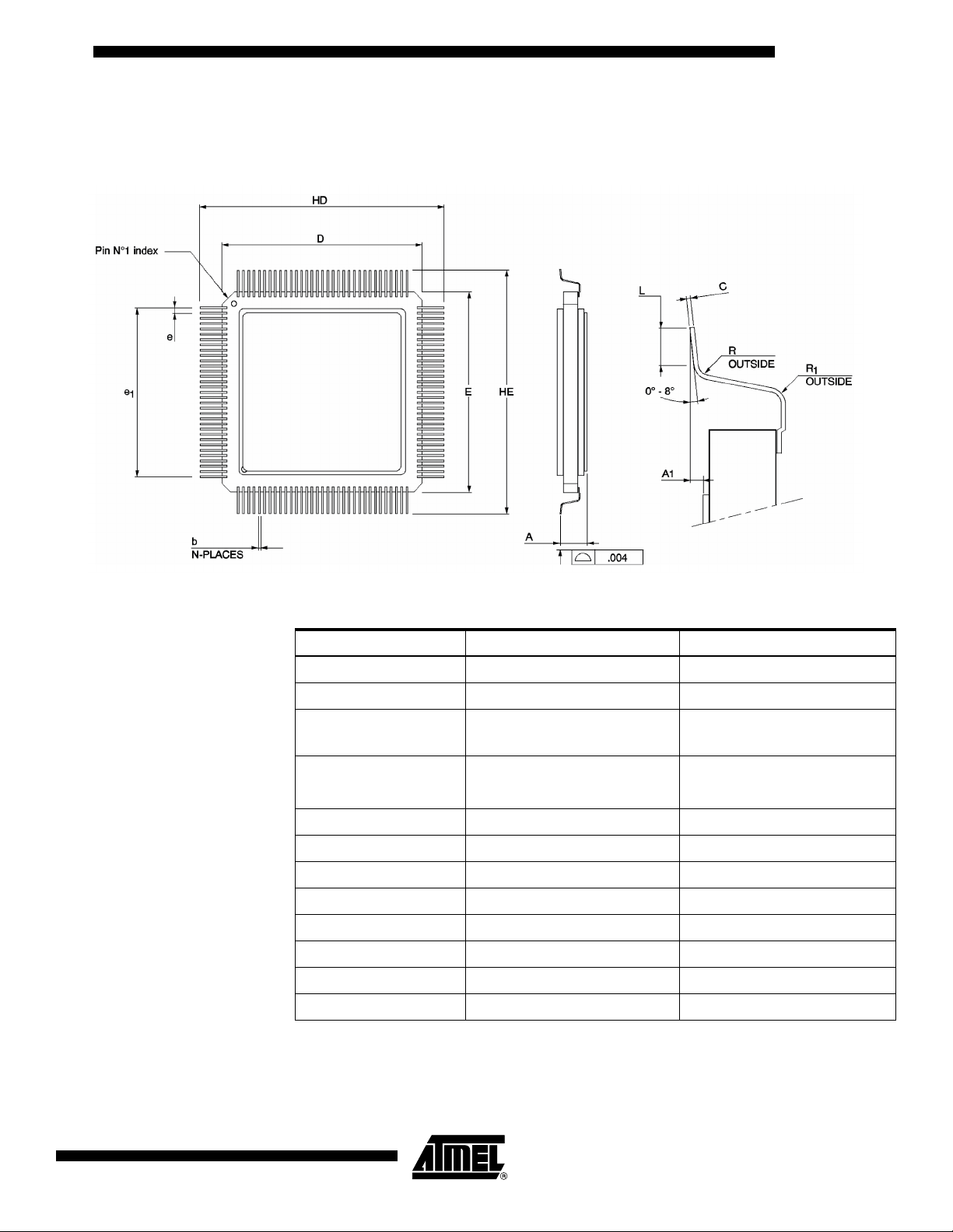
196 pins – Gullwing
CQFP cavity up
TS68040
* Reduce pin count shown for clarity, 49 pins per side
Symbol Millimeters Inches
A 4.19 max 0.165 max
A1 0.673 ± 0.2 .0265 ±.008
b
c
D/E 33.91 ±0.25 1.335 ±.01
e .635 BSC .025 BSC
e1 30.48 ±0.13 1.2 ±.005
HD/HE 38.8 ±0.18 1.528 ±.007
L 0.813 ±0.2 .032 ±.008
N 196 196
R 0.55 ±0.25 .022 ±.01
R1 0.23 min .009 min
0.23 +0.05
0.23 -0.038
0.127 +0.05 .005 +.002
0.127 -0.025 .005 -.001
.009 +.002
.009 -.0015
2116A–HIREL–09/02
45

Ordering Information
MIL-STD-883 C and
Internal Standard
Device
Temperature range:
M: Tc = -55; Tj = +125°C
V: Tc = -40; Tj = +110°C
Package:
F: CQFP/Gullwing leads
R: PGA
FT: CQFP Flat tie-bar
Notes: 1. On request.
2. Standard process.
3. Non request for small quantity.
(3)
Standard lead finish
DESC Drawing 5962-93143
Gold
Gold
Gold
TS68040
TS68040
R 1B/C25 A
M
DESC
01 XA
Revision level
Operating frequency:
25: 25 MHz
33: 33 MHz
Screening level:
B/C: MIL-STD-883, class B
D/T: Internal standard with burn-in
U: Upscreening
U/T: Upscreening + burn-in
___: Internal standard
Lead finish:
1: Hot solder dip
__: Gold
A
(2)
(1)
46
Device
DESC Screening
Speed:
01: 25 MHz
02: 33 MHz
TS68040
Revision level
Lead finish:
A: Hot solder dip
C: Gold
Package:
X: PGA
Y: CQFP Flat tie-bar
Z: CQFP Gullwing leads
2116A–HIREL–09/02

Detailed TS68040 Part
List
Hi-REL Product
TS68040
Commercial Atmel
Part Number Norms Package Temperature range (°C)
TS68040MRB/C25A MIL-STD-883 PGA 179 T
TS68040MRB/C33A MIL-STD-883 PGA 179 T
TS68040MFB/C25A MIL-STD-883 CQFP 196 T
TS68040MFB/C33A MIL-STD-883 CQFP 196 T
TS68040DESC01XAA DESC PGA 179 tin T
TS68040DESC02XAA DESC PGA 179 tin T
TS68040DESC01XCA DESC PGA 179 gold T
TS68040DESC02XCA DESC PGA 179 gold T
TS68040DESC01YCA DESC
TS68040DESC02YCA DESC
TS68040DESC01ZAA DESC
TS68040DESC01ZCA DESC
TS68040DESC02ZAA DESC
CQFP 196 tie
bar gold
CQFP 196 tie
bar gold
CQFP 196
gullwing tin
CQFP 196
gullwing gold
CQFP 196
gullwing tin
= -55/+TJ= +125 25 Atmel datasheet
C
= -55/+TJ= +125 33 Atmel datasheet
C
= -55/+TJ= +125 25 Atmel datasheet
C
= -55/+TJ= +125 33 Atmel datasheet
C
= -55/+TJ= +125 25 5962-9314301MXA
C
= -55/+TJ= +125 33 5962-9314302MXA
C
= -55/+TJ= +125 25 5962-9314301MXC
C
= -55/+TJ= +125 33 5962-9314302MXC
C
T
= -55/+TJ= +125 25 5962-9314301MYC
C
T
= -55/+TJ= +125 33 5962-9314302MYC
C
= -55/+TJ= +125 25 5962-9314301MZA
T
C
= -55/+TJ= +125 25 5962-9314301MZC
T
C
T
= -55/+TJ= +125 33 5962-9314302MZA
C
Frequency
(MHz) Drawing number
TS68040DESC02ZCA DESC
CQFP 196
gullwing gold
TS68040MFB/C25A MIL-STD-883 CQFP 196 T
TS68040MFB/C33A MIL-STD-883 CQFP 196 T
TS68040MRD/T25A BURN IN PGA 179 T
TS68040MRD/T33A BURN IN PGA 179 T
TS68040MFD/T25A BURN IN CQFP 196 T
TS68040MFD/T33A BURN IN CQFP 196 T
= -55/+TJ= +125 33 5962-9314302MZC
T
C
= -55/+TJ= +125 25 Atmel datasheet
C
= -55/+TJ= +125 33 Atmel datasheet
C
= -55/+TJ= +125 25 Atmel datasheet
C
= -55/+TJ= +125 33 Atmel datasheet
C
= -55/+TJ= +125 25 Atmel datasheet
C
= -55/+TJ= +125 33 Atmel datasheet
C
2116A–HIREL–09/02
47

Standard Product
Commercial Atmel
Part Number Norms Package Temperature Range (°C)
TS68040VR25A Atmel standard PGA 179 T
TS68040VR33A Atmel standard PGA 179 T
TS68040MR25A Atmel standard PGA 179 T
TS68040MR33A Atmel standard PGA 179 T
TS68040VF25A Atmel standard CQFP 196 T
TS68040VF33A Atmel standard CQFP 196 T
TS68040MF25A Atmel standard CQFP 196 T
TS68040MF33A Atmel standard CQFP 196 T
= -40/+TJ= +110 25 Atmel datasheet
C
= -40/+TJ= +110 33 Atmel datasheet
C
= -55/+TJ= +125 25 Atmel datasheet
C
= -55/+TJ= +125 33 Atmel datasheet
C
= -40/+TJ= +110 25 Atmel datasheet
C
= -40/+TJ= +110 33 Atmel datasheet
C
= -55/+TJ= +125 25 Atmel datasheet
C
= -55/+TJ= +125 33 Atmel datasheet
C
Note: FT: available on request.
Frequency
(MHz) Drawing Number
48
TS68040
2116A–HIREL–09/02

Atmel Headquarters Atmel Operations
Corporate Headquarters
2325 Orchard Parkway
San Jose, CA 95131
TEL 1(408) 441-0311
FAX 1(408) 487-2600
Europe
Atmel Sarl
Route des Arsenaux 41
Case Postale 80
CH-1705 Fribourg
Switzerland
TEL (41) 26-426-5555
FAX (41) 26-426-5500
Asia
Room 1219
Chinachem Golden Plaza
77 Mody Road Tsimhatsui
East Kowloon
Hong Kong
TEL (852) 2721-9778
FAX (852) 2722-1369
Japan
9F, Tonetsu Shinkawa Bldg.
1-24-8 Shinkawa
Chuo-ku, Tokyo 104-0033
Japan
TEL (81) 3-3523-3551
FAX (81) 3-3523-7581
Memory
2325 Orchard Parkway
San Jose, CA 95131
TEL 1(408) 441-0311
FAX 1(408) 436-4314
Microcontrollers
2325 Orchard Parkway
San Jose, CA 95131
TEL 1(408) 441-0311
FAX 1(408) 436-4314
La Chantrerie
BP 70602
44306 Nantes Cedex 3, France
TEL (33) 2-40-18-18-18
FAX (33) 2-40-18-19-60
ASIC/ASSP/Smart Cards
Zone Industrielle
13106 Rousset Cedex, France
TEL (33) 4-42-53-60-00
FAX (33) 4-42-53-60-01
1150 East Cheyenne Mtn. Blvd.
Colorado Springs, CO 80906
TEL 1(719) 576-3300
FAX 1(719) 540-1759
Scottish Enterprise Technology Park
Maxwell Building
East Kilbride G75 0QR, Scotland
TEL (44) 1355-803-000
FAX (44) 1355-242-743
RF/Automotive
Theresienstrasse 2
Postfach 3535
74025 Heilbronn, Germany
TEL (49) 71-31-67-0
FAX (49) 71-31-67-2340
1150 East Cheyenne Mtn. Blvd.
Colorado Springs, CO 80906
TEL 1(719) 576-3300
FAX 1(719) 540-1759
Biometrics/Imaging/Hi-Rel MPU/
High Speed Converters/RF Datacom
Avenue de Rochepleine
BP 123
38521 Saint-Egreve Cedex, France
TEL (33) 4-76-58-30-00
FAX (33) 4-76-58-34-80
e-mail
literature@atmel.com
Web Site
http://www.atmel.com
© Atmel Corporation 2002.
Atmel Corporation makes no warranty for the use of its products, other than those expressly contained in the Company’s standard warranty
whichisdetailedinAtmel’s Terms and Conditions located on the Company’s web site. The Company assumes no responsibility for any errors
which may appear in this document, reserves the right to change devices or specifications detailed herein at any time without notice, and does
not make any commitment to update the information contained herein. No licenses to patents or other intellectual property of Atmel are granted
by the Company in connection with the sale of Atmel products, expressly or by implication. Atmel’s products are not authorized for use as critical
components in life support devices or systems.
AT ME L®is the trademarks of Atmel.
®
UNIX
is a Registered Trademark of AT&T Bell Laboratories.
Other terms and product names may be the trademarks of others.
Printed on recycled paper.
2116A–HIREL–09/02 0M
 Loading...