


查询T89C51RB2-3CBCL供应商
T89C51RB2/RC2
8-bit Microcontroller with 16 Kbytes/ 32 Kbytes FLASH
1. Description
T89C51RB2/RC2 is a high performance FLASH version
of the 80C51 8-bit microcontrollers. It contains a 16K
or 32Kbytes Flash memory block for program and data.
The 16 Kbytes or 32 Kbytes FLASH memory can be
programmed either in parallel mode or in serial mode
with the ISP capability or with software. The
programming voltage is internally generated from the
standard V
The T89C51RB2/RC2 retains all features of the 80C52
with 256 bytes of internal RAM, a 7-source 4-level
interrupt controller and three timer/counters.
In addition, the T89C51RB2/RC2 has a Programmable
Counter Array, an XRAM of 1024 byte, a Hardware
Watchdog Timer, a Keyboard Interface, a SPI Interface,
a more versatile serial channel that facilitates
multiprocessor communication (EUART) and a speed
improvement mechanism (X2 mode).
CC
pin.
2. Features
• 80C52 Compatible
• 8051 pin and instruction compatible
• Four 8-bit I/O ports
• Three 16-bit timer/counters
• 256 bytes scratch pad RAM
• 10 Interrupt sources with 4 priority levels
• Dual Data Pointer
• Variable length MOVX for slow RAM/peripherals
• ISP (In System Programming) using standard V
power supply.
• Boot ROM contains low level FLASH programming
routines and a default serial loader
• High-Speed Architecture
• 40 MHz in standard mode
• 20 MHz in X2 mode (6 clocks/machine cycle)
• 16K/32K bytes on-chip FLASH program / data
Memory
• Byte and page (128 bytes) erase and write
• 100k write cycles
CC
Pinout is the standard 40/44 pins of the C52.
The fully static design of the T89C51RB2/RC2 allows
to reduce system power consumption by bringing the
clock frequency down to any value, even DC, without
loss of data.
The T89C51RB2/RC2 has 2 software-selectable modes
of reduced activity and 8 bit clock prescaler for further
reduction in power consumption. In the Idle mode the
CPU is frozen while the peripherals and the interrupt
system are still operating. In the power-down mode the
RAM is saved and all other functions are inoperative.
The added features of the T89C51RB2/RC2 make it more
powerful for applications that need pulse width
modulation, high speed I/O and counting capabilities
such as alarms, motor control, corded phones, smart card
readers.
• On-chip 1024 bytes expanded RAM (XRAM)
• Software selectable size (0, 256, 512, 768, 1024
bytes)
• 256 bytes selected at reset for TS87C51RB2/RC2
compatibility
• Keyboard interrupt interface on port P1
• SPI Interface (Master / Slave Mode)
• 8-bit clock prescaler
• Improved X2 mode with independant selection for
CPU and each peripheral
• Programmable Counter Array 5 Channels with:
• High Speed Output,
• Compare / Capture,
• Pulse Width Modulator,
• Watchdog Timer Capabilities
• Asynchronous port reset
• Full duplex Enhanced UART
• Dedicated Baud Rate Generator for UART
• Low EMI (inhibit ALE)
Rev. B - 30-Mar-01
Preliminary
1
T89C51RB2/RC2
• Hardware Watchdog Timer (One-time enabled with Reset-Out)
• Power control modes:
• Idle Mode.
• Power-down mode.
-50µA at 3V
- 100µA Commercial at 5V
- 150µA Industrial at 5V
• Power-Off Flag.
• Power supply: 4.5 to 5.5V or 2.7 to 3.6V
• Temperature ranges: Commercial (0 to +70°C) and industrial (-40°C to +85°C).
• Packages: PDIL40, PLCC44, VQFP44
Table 1. Memory Size
T89C51RB2 16k 1024 1280 32
T89C51RC2 32k 1024 1280 32
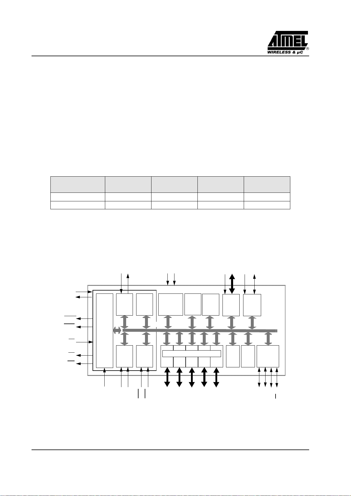
3. Block Diagram
XTAL1
XTAL2
ALE/
PROG
PSEN
EA
Flash (bytes) XRAM (bytes)
RxD
TxD
(2)(2)
EUART
BRG
CPU
RAM
+
256x8
C51
CORE
IB-bus
CC
V
Flash
32Kx8 or
16Kx8
TOTAL RAM
(bytes)
Vss
1Kx8
Boot
ROM
2Kx8
XRAM
(1)
ECI
PCA
PCA
(1)
(1) (1)
T2EX
Timer2
I/O
T2
RD
WR
(2)
(2)
Timer 0
Timer 1
(2) (2) (2) (2)
RESET
INT
Ctrl
T0
T1
INT1
INT0
(1): Alternate function of Port 1
(2): Alternate function of Port 3
2
Parallel I/O Ports & Ext. Bus
Port 0
P0
Port 1
P1
Port 2
Port 3
P2
P3
Port I2
PI2
Watch
Dog
Key
Board
SPI
(1) (1) (1)
(1)
MISO
SS
MOSI
SCK
Rev. B - 30-Mar-01
Preliminary

T89C51RB2/RC2
4. SFR Mapping
The Special Function Registers (SFRs) of the T89C51RB2/RC2 fall into the following categories:
• C51 core registers: ACC, B, DPH, DPL, PSW, SP
• I/O port registers: P0, P1, P2, P3
• Timer registers: T2CON, T2MOD, TCON, TH0, TH1, TH2, TMOD, TL0, TL1, TL2, RCAP2L, RCAP2H
• Serial I/O port registers: SADDR, SADEN, SBUF, SCON
• PCA ( Programmable Counter Array ) registers : CCON , CCAPMx , CL , CH , CCAPxH , CCAPxL (x : 0 to 4)
• Power and clock control registers: PCON
• Hardware Watchdog Timer registers : WDTRST, WDTPRG
• Interrupt system registers: IE0, IPL0, IPH0 , IE1 , IPL1 , IPH1
• Keyboard Interface registers : KBE , KBF , KBLS
• SPI registers : SPCON , SPSTR , SPDAT
• BRG ( Baud Rate Generator ) registers : BRL , BDRCON
• Flash register : FCON
• Clock Prescaler register : CKRL
• Others: AUXR, AUXR1 , CKCON0 , CKCON1
Rev. B - 30-Mar-01
Preliminary
3

T89C51RB2/RC2
Table 2. Sfr mapping
Table below shows all SFRs with their address and their reset value.
Bit
Non Bit addressable
addressable
0/8 1/9 2/A 3/B 4/C 5/D 6/E 7/F
F8h
F0h
E8h
E0h
D8h
D0h
C8h
C0h
B8h
B0h
A8h
A0h
98h
90h
88h
80h
B
0000 0000
ACC
0000 0000
CCON
00X0 0000
PSW
0000 0000
T2CON
0000 0000
IPL0
X000 000
P3
1111 1111
IE0
0000 0000
P2
1111 1111
SCON
0000 0000
P1
1111 1111
TCON
0000 0000
P0
1111 1111SP0000 0111
0/8 1/9 2/A 3/B 4/C 5/D 6/E 7/F
CH
0000 0000
CL
0000 0000
CMOD
00XX X000
FCON (1)
XXXX 0000
T2MOD
XXXX XX00
SADEN
0000 0000
IE1
XXXX X000
SADDR
0000 0000
SBUF
XXXX XXXX
TMOD
0000 0000
CCAP0H
XXXX XXXX
CCAP0L
XXXX XXXX
CCAPM0
X000 0000
RCAP2L
0000 0000
IPL1
XXXX X000
AUXR1
XXXX X0X0
BRL
0000 0000
TL0
0000 0000
DPL
0000 0000
CCAP1H
XXXX XXXX
CCAP1L
XXXX XXXX
CCAPM1
X000 0000
RCAP2H
0000 0000
SPCON
0001 0100
IPH1
XXXX X111
BDRCON
XXX0 0000
TL1
0000 0000
DPH
0000 0000
CCAPL2H
XXXX XXXX
CCAPL2L
XXXX XXXX
CCAPM2
X000 0000
TL2
0000 0000
SPSTA
0000 0000
KBLS
0000 0000
TH0
0000 0000
CCAPL3H
XXXX XXXX
CCAPL3L
XXXX XXXX
CCAPM3
X000 0000
TH2
0000 0000
SPDAT
XXXX XXXX
KBE
0000 0000
TH1
0000 0000
CCAPL4H
XXXX XXXX
CCAPL4L
XXXX XXXX
CCAPM4
X000 0000
WDTRST
XXXX XXXX
KBF
0000 0000
AUXR
XX0X 0000
IPH0
X000 0000
CKCON1
XXXX XXX0
WDTPRG
XXXX X000
CKRL
1111 1111
CKCON0
0000 0000
PCON
00X1 0000
FFh
F7h
EFh
E7h
DFh
D7h
CFh
C7h
BFh
B7h
AFh
A7h
9Fh
97h
8Fh
87h
reserved
(1) FCON access is reserved for the FLASH API and ISP software.
4
Preliminary
Rev. B - 30-Mar-01

5. Pin Configurations
T89C51RB2/RC2
P1.0/T2
P1.1/T2EX/SS
P1.2/ECI
P1.3CEX0
P1.4/CEX1
P1.5/CEX2/MISO
P1.6/CEX3/SCK
P1.7CEX4/MOSI
RST
P3.0/RxD
P3.1/TxD
P3.2/INT0
P3.3/INT1
P3.4/T0
P3.5/T1
P3.6/WR
P3.7/RD
XTAL2
XTAL1
VSS
1
3
4
5
9
10
11
12
13
14
15
16
17
2
6
7
8
18
19
20
PDIL40
40
39
38
37
36
35
34
33
32
31
30
29
28
27
26
25
24
23
22
21
VCC
P0.0/AD0
P0.1/AD1
P0.2/AD2
P0.3/AD3
P0.4/AD4
P0.5/AD5
P0.6/AD6
P0.7/AD7
EA
ALE/PROG
PSEN
P2.7/AD15
P2.6/AD14
P2.5/AD13
P2.4/AD12
P2.3/AD11
P2.2/AD10
P2.1/AD9
P2.0/AD8
P1.5/CEX2/MISO
P1.6/CEX3/SCK
P1.7/CEx4/MOSI
RST
P3.0/RxD
NIC*
P3.1/TxD
P3.2/INT0
P3.3/INT1
P3.4/T0
P3.5/T1
P1.4/CEX1
P1.3/CEX0
5 4 3 2 1 6
7
8
9
10
11
12
13
14
15
16
17
18 19 23222120 262524 27 28
P1.1/T2EX/SS
P1.2/ECI
P1.0/T2
NIC*
VCC
44 43 42 41 40
PLCC44
P0.0/AD0
P0.1/AD1
P0.2/AD2
P0.3/AD3
39
38
37
36
35
34
33
32
31
30
29
P0.4/AD4
P0.5/AD5
P0.6/AD6
P0.7/AD7
EA
NIC*
ALE/PROG
PSEN
P2.7/A15
P2.6/A14
P2.5/A13
P1.5/CEX2/MISO
P1.6/CEX3/SC K
P1.7/CEX4/MOSI
P3.0/RxD
NIC*
P3.1/TxD
P3.2/INT0
P3.3/INT1
P3.4/T0
P3.5/T1
*NIC: No Internal Connection
RST
1
3
4
5
9
10
11
2
6
7
8
P1.4/CEX1
43 42 41 40 3944 38 37 36 35 34
12 13 17161514 201918 21 22
P3.6/ WR
P1.1/T2EX/SS
P1.3/CEX0
P1.2/ECI
VQFP44 1.4
XTAL1
XTAL2
P3.7/RD
P1.0/T2
VSS
NIC*
VCC
P0.0/AD0
NIC*
P2.0/ A8
P2.1/A9
NIC*
VSS
XTAL2
P0.2/AD2
P0.3/AD3
P0.1/AD1
P0.4/AD4
33
32
P0.5/AD5
31
P0.6/AD6
30
P0.7/AD7
29
EA
28
NIC*
27
ALE/PROG
26
PSEN
25
P2.7/A15
24
P2.6/A14
23
P2.5/A13
P2.3/ A11
P2.2/ A10
P2.4/ A12
P3.6/WR
XTAL1
P3.7/RD
P2.0/A8
P2.1/A9
P2.2/A10
P2.3/A11
P2.4/A12
Rev. B - 30-Mar-01
Preliminary
5

T89C51RB2/RC2
Table 3. Pin Description for 40/44 pin packages
Pin Number
Mnemonic
V
SS
V
CC
P0.0-P0.7 39-32 43-36 37-30 I/O Port 0: Port 0 is an open-drain, bidirectional I/O port. Port 0 pins that
P1.0-P1.7 1-8 2-9 40-44
XTAL1 19 21 15 I
XTAL2 18 20 14 O Crystal 2: Output from the inverting oscillator amplifier
DIL LCC
20 22 16 I Ground: 0V reference
40 44 38 I
12 40 I/OP1.0 : Input / Output
23 41 I/OP1.1 : Input / Output
34 42 I/OP1.2 : Input / Output
45 43 I/OP1.3: Input / Output
56 44 I/OP1.4 : Input / Output
67 1 I/OP1.5 : Input / Output
78 2 I/OP1.6 : Input / Output
89 3 I/OP1.7 : Input / Output:
VQFP44
1.4
1-3
Type Name and Function
Power Supply: This is the power supply voltage for normal, idle and
power-down operation
have 1s written to them float and can be used as high impedance inputs.
Port 0 must be polarized to V
current consumption. Port 0 is also the multiplexed low-order address
and data bus during access to external program and data memory. In this
application, it uses strong internal pull-up when emitting 1s. Port 0 also
inputs the code bytes during FLASH programming. External pull-ups are
required during program verification during which P0 outputs the code
bytes.
I/O Port 1: Port 1 is an 8-bit bidirectional I/O port with internal pull-ups.
Port 1 pins that have 1s written to them are pulled high by the internal
pull-ups and can be used as inputs. As inputs, Port 1 pins that are
externally pulled low will source current because of the internal pullups. Port 1 also receives the low-order address byte during memory
programming and verification.
Alternate functions for T89C51RB2/RC2 Port 1 include:
I/O T2 (P1. 0): Timer/Counter 2 external count input/Clockout
I T2EX : Timer/Counter 2 Reload/Capture/Direction Control
I SS
I ECI : External Clock for the PCA
I/O CEX0 : Capture/Compare External I/O for PCA module 0
I/O CEX1 : Capture/Compare External I/O for PCA module 1
I/O CEX2 : Capture/Compare External I/O for PCA module 2
I/O MISO : SPI Master Input Slave Output line
I/O CEX3 : Capture/Compare External I/O for PCA module 3
I/O SCK : SPI Serial Clock
I/O CEX4 : Capture/Compare External I/O for PCA module 4
I/O MOSI : SPI Master Output Slave Input line
: SPI Slave Select
When SPI is is in master mode , MISO receives data from the slave
peripheral. When SPI is in slave mode , MISO outputs data to the master
controller.
SCK outputs clock to the slave peripheral
When SPI is is in master mode , MOSI outputs data to the slave peripheral.
When SPI is in slave mode , MOSI receives data from the master
controller.
Crystal 1: Input to the inverting oscillator amplifier and input to the
internal clock generator circuits.
or VSS in order to prevent any parasitic
CC
6
Rev. B - 30-Mar-01
Preliminary

T89C51RB2/RC2
Pin Number
Mnemonic
P2.0-P2.7 21-28 24-31 18-25 I/O Port 2: Port 2 is an 8-bit bidirectional I/O port with internal pull-ups.
P3.0-P3.7 10-17 11,
RST 9 10 4 I/O
ALE/PROG
PSEN 29 32 26 O Program Strobe ENable: The read strobe to external program memory.
EA 31 35 29 I External Access Enable: EA
DIL LCC
10 11 5 I RXD (P3.0): Serial input port
11 13 7 O TXD (P3.1): Serial output port
12 14 8 I INT0
13 15 9 I INT1
14 16 10 I T0 (P3.4): Timer 0 external input
15 17 11 I T1 (P3.5): Timer 1 external input
16 18 12 O WR
17 19 13 O RD
30 33 27 O (I) Address Latch Enable/Program Pulse: Output pulse for latching the
VQFP44
1.4
13-195,7-13
Type Name and Function
Port 2 pins that have 1s written to them are pulled high by the internal
pull-ups and can be used as inputs. As inputs, Port 2 pins that are
externally pulled low will source current because of the internal pullups. Port 2 emits the high-order address byte during fetches from external
program memory and during accesses to external data memory that use
16-bit addresses (MOVX @DPTR).In this application, it uses strong
internal pull-ups emitting 1s. During accesses to external data memory
that use 8-bit addresses (MOVX @Ri), port 2 emits the contents of the
P2 SFR. Some Port 2 pins receive the high order address bits during
EPROM programming and verification:
P2.0 to P2.5 for 16Kb devices
P2.0 to P2.6 for 32Kb devices
I/O Port 3: Port 3 is an 8-bit bidirectional I/O port with internal pull-ups.
Port 3 pins that have 1s written to them are pulled high by the internal
pull-ups and can be used as inputs. As inputs, Port 3 pins that are
externally pulled low will source current because of the internal pullups. Port 3 also serves the special features of the 80C51 family, as listed
below.
(P3.2): External interrupt 0
(P3.3): External interrupt 1
(P3.6): External data memory write strobe
(P3.7): External data memory read strobe
Reset: A high on this pin for two machine cycles while the oscillator is
running, resets the device. An internal diffused resistor to V
a power-on reset using only an external capacitor to V
an output when the hardware watchdog forces a system reset.
low byte of the address during an access to external memory. In normal
operation, ALE is emitted at a constant rate of 1/6 (1/3 in X2 mode) the
oscillator frequency, and can be used for external timing or clocking.
Note that one ALE pulse is skipped during each access to external data
memory. This pin is also the program pulse input (PROG
programming. ALE can be disabled by setting SFR’s AUXR.0 bit. With
this bit set, ALE will be inactive during internal fetches.
When executing code from the external program memory, PSEN
activated twice each machine cycle, except that two PSEN
are skipped during each access to external data memory. PSEN
activated during fetches from internal program memory.
device to fetch code from external program memory locations 0000H to
FFFFH (RD). If security level 1 is programmed, EA
latched on Reset.
must be externally held low to enable the
will be internally
permits
SS
. This pin is
CC
) during Flash
activations
is not
is
Rev. B - 30-Mar-01
Preliminary
7

6. Ordering Information
T89C51RB2/RC2
T
89C51RC2 ( 32k Flash )
89C51RB2 ( 16k Flash )
89C51Rx2
-3C
Packages:
3C: PDIL40
SL: PLCC44
RL: VQFP44 (1.4mm)
S
Conditioning
S: Stick
T: Tra y
B: Blue Tape
W: Wafe r
C
Temperature Range
C:Commercial 0 to 70
I:Industrial -40 to 85
o
C
o
C
-M: VCC: 5V
-L: VCC: 3 V
M
40 MHz, X1 mode
20 MHz, X2 mode
40 MHz, X1 mode
20 MHz, X2 mode
Rev. B - 30-Mar-01
Preliminary
8
T89C51RB2/RC2
Table 4. Possible order entries
Exten-
sion
-3CSCM Stick, PDIL40, Com, 5V
-3CSIM Stick, PDIL40, Ind, 5V
-SLSCM Stick, PLCC44, Com, 5V
-SLSIM Stick, PLCC44, Ind, 5V
-SLSCL Stick, PLCC44, Com, 3V
-SLSIL Stick, PLCC44, Ind, 3V
-RLTIM Tray, VQFP44, Ind, 5V
-RLTCL Tray, VQFP44, Com, 3V
-SLSEM Stick, PLCC44, Sample, 5V
Type T89C51RB2 T89C51RC2
X X
X X
X X
X X
X X
X X
X X
X X
X X
9
Rev. B - 30-Mar-01
Preliminary
 Loading...