


Appendix A – ATtiny24A/44A Specification at 105°C
This document contains information specific to devices operating at temperatures up
to 105°C. Only deviations are covered in this appendix, all other information can be
found in the complete datasheet. The complete datasheet can be found at
www.atmel.com.
8-bit
Microcontroller
with 2K/4K
Bytes In-System
Programmable
Flash
ATtiny24A
ATtiny44A
Appendix A
Rev. 8183D-Appendix A–AVR–08/11

1. Memories
1.1 EEPROM Data Memory
The EEPROM has an endurance of at least 50,000 write/erase cycles.
2
ATtiny24A/44A
8183D-Appendix A–AVR–08/11

2. Electrical Characteristics
2.1 Absolute Maximum Ratings*
ATtiny24A/44A
Operating Temperature.................................. -55°C to +125°C
*NOTICE: Stresses beyond those listed under “Absolute
Maximum Ratings” may cause permanent dam-
Storage Temperature..................................... -65°C to +150°C
age to the device. This is a stress rating only and
functional operation of the device at these or
Voltage on any Pin except RESET
with respect to Ground ................................-0.5V to VCC+0.5V
other conditions beyond those indicated in the
operational sections of this specification is not
implied. Exposure to absolute maximum rating
Voltage on RESET
with respect to Ground......-0.5V to +13.0V
conditions for extended periods may affect
device reliability.
Maximum Operating Voltage ............................................ 6.0V
DC Current per I/O Pin............................................... 40.0 mA
DC Current V
and GND Pins ................................ 200.0 mA
CC
2.2 DC Characteristics
Table 2-1. DC Characteristics. TA = -40°C to +105°C
Symbol Parameter Condition Min Typ
V
= 1.8V - 2.4V -0.5 0.2V
Input Low Voltage
V
IL
Input Low Voltage,
Pin as Reset
RESET
(4)
Input High-voltage
Except RESET pin
V
IH
Input High-voltage
pin as Reset
RESET
V
OL
V
OH
I
LIL
I
LIH
Output Low Voltage
Except RESET pin
Output High-voltage
Except RESET pin
Input Leakage
Current I/O Pin
Input Leakage
Current I/O Pin
(4)
(5)
(7)
(6)
(7)
CC
V
= 2.4V - 5.5V -0.5 0.3V
CC
VCC = 1.8V - 5.5 -0.5 0.2V
= 1.8V - 2.4V 0.7V
V
CC
= 2.4V - 5.5V 0.6V
V
CC
VCC = 1.8V to 5.5V 0.9V
CC
CC
CC
(2)
(2)
(2)
IOL = 10 mA, VCC = 5V 0.6 V
= 5 mA, VCC = 3V 0.5 V
I
OL
IOH = -10 mA, VCC = 5V 4.3 V
= -5 mA, VCC = 3V 2.5 V
I
OH
Vcc = 5.5V, pin low
(absolute value)
Vcc = 5.5V, pin high
(absolute value)
(1)
Max Units
VCC +0.5 V
VCC +0.5 V
VCC +0.5 V
< 0.05 1
< 0.05 1
(8)
(8)
CC
CC
CC
(3)
(3)
(3)
V
V
µA
µA
R
Pull-up Resistor, I/O Pin VCC = 5.5V, input low 20 50 kΩ
PU
8183D-Appendix A–AVR–08/11
Pull-up Resistor, Reset Pin V
= 5.5V, input low 30 60 kΩ
CC
3

Table 2-1. DC Characteristics. TA = -40°C to +105°C (Continued)
4 MHz
1.8V 5.5V
4.5V
20 MHz
Symbol Parameter Condition Min Typ
f = 1MHz, VCC = 2V 0.25 0.5 mA
Supply Current,
Active Mode
I
CC
Supply Current,
Idle Mode
Supply Current,
Power-Down Mode
(9)
(9)
(10)
Notes: 1. Typical values at 25°C.
2. “Min” means the lowest value where the pin is guaranteed to be read as high.
3. “Max” means the highest value where the pin is guaranteed to be read as low.
4. Not tested in production.
5. Although each I/O port can sink more than the test conditions (10 mA at V
conditions (non-transient), the sum of all I
may exceed the related specification. Pins are not guaranteed to sink current greater than the listed test condition.
6. Although each I/O port can source more than the test conditions (10 mA at V
conditions (non-transient), the sum of all I
may exceed the related specification. Pins are not guaranteed to source current greater than the listed test condition.
7. The RESET
pin must tolerate high voltages when entering and operating in programming modes and, as a consequence,
has a weak drive strength as compared to regular I/O pins. See Figure 3-25, Figure 3-26, Figure 3-27, and Figure 3-28
(starting on page 22).
8. These are test limits, which account for leakage currents of the test environment. Actual device leakage currents are lower.
9. Values are with external clock using methods described in “Minimizing Power Consumption”. Power reduction is enabled
(PRR = 0xFF) and there is no I/O drive.
10.BOD disabled.
f = 4MHz, V
f = 8MHz, V
f = 1MHz, VCC = 2V 0.04 0.2 mA
f = 4MHz, V
f = 8MHz, V
WDT enabled, VCC = 3V 4 20 µA
WDT disabled, V
= 3V 1.2 2 mA
CC
= 5V 4.4 7 mA
CC
= 3V 0.25 0.6 mA
CC
= 5V 1.3 2 mA
CC
= 3V 0.2 10 µA
CC
= 5V, 5 mA at VCC = 3V) under steady state
(for all ports) should not exceed 60 mA. If IOL exceeds the test conditions, VOL
OL
(for all ports) should not exceed 60 mA. If IOH exceeds the test condition, VOH
OH
CC
= 5V, 5 mA at VCC = 3V) under steady state
CC
(1)
Max Units
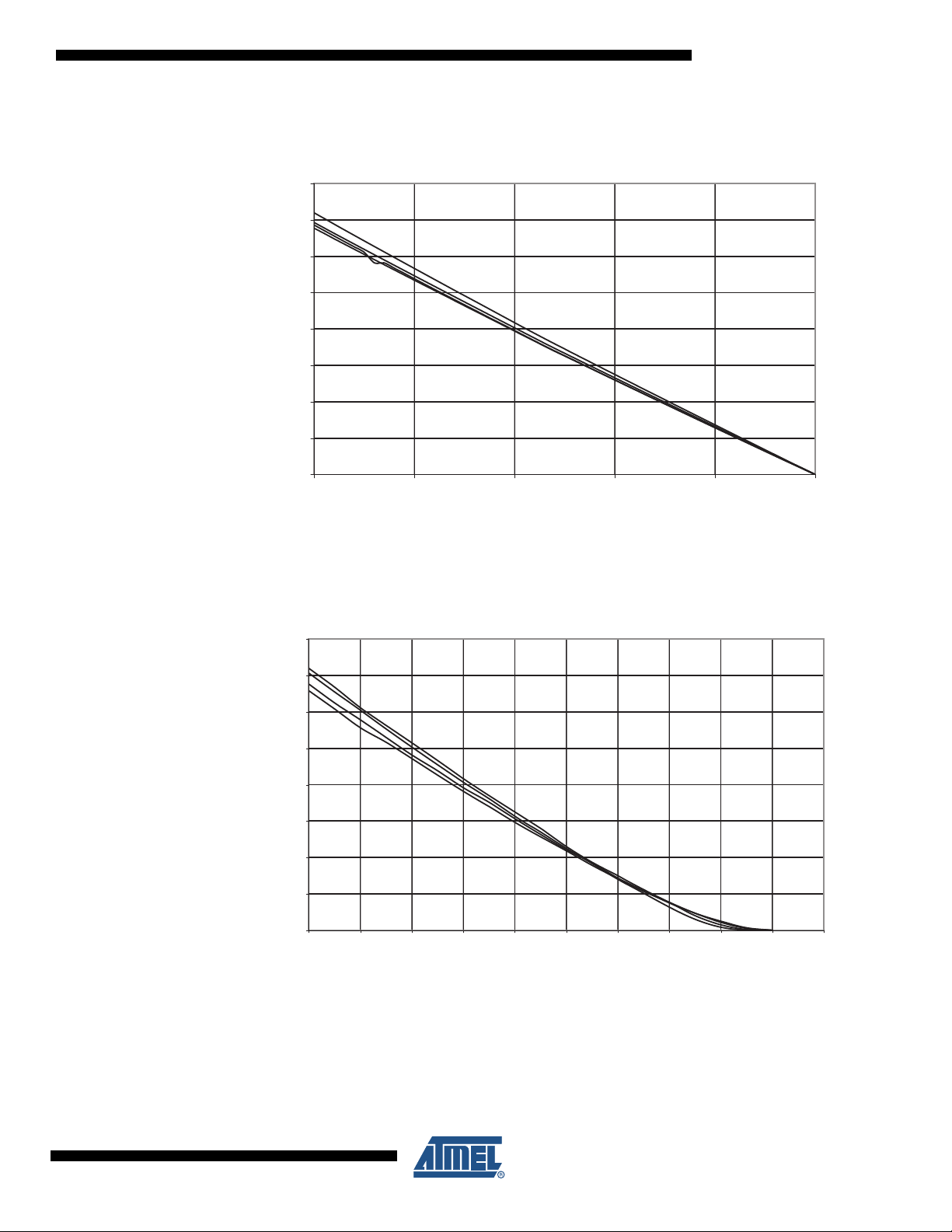
2.3 Speed
4
ATtiny24A/44A
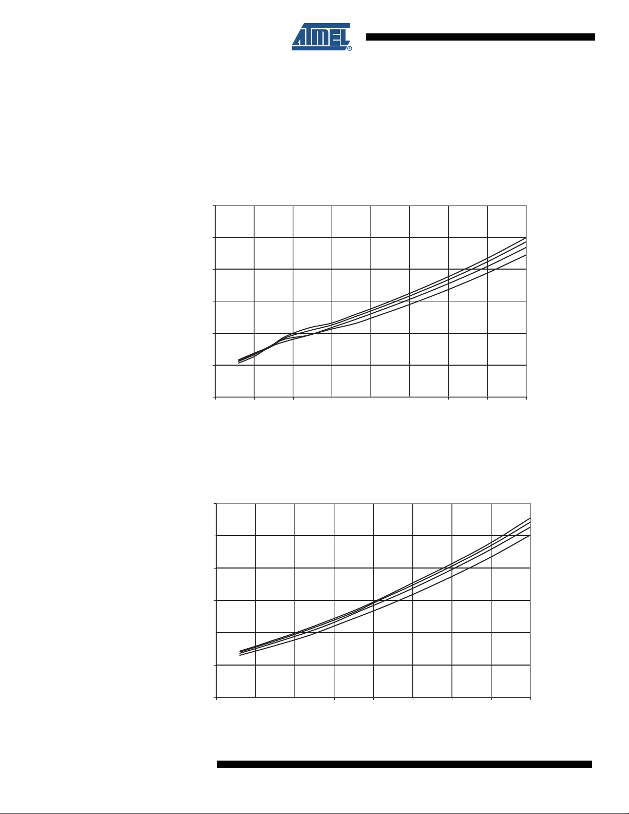
The maximum operating frequency of the device depends on V
relationship between maximum frequency and V
Figure 2-1. Maximum Frequency vs. V
. TA = -40°C to +105°C
CC
is linear in the region 1.8V < VCC < 4.5V.
CC
As shown in Figure 2-1, the
CC.
8183D-Appendix A–AVR–08/11
2.4 Clock Characteristics
2.4.1 Accuracy of Calibrated Internal Oscillator
It is possible to manually calibrate the internal oscillator to be more accurate than default factory
calibration. Note that the oscillator frequency depends on temperature and voltage. Voltage and
temperature characteristics can be found in Figure 3-46 on page 32.
Table 2-2. Calibration Accuracy of Internal RC Oscillator
ATtiny24A/44A
Calibration
Method Target Frequency V
Factory
Calibration
User
Calibration
8.0 MHz 3V 25°C±10%
Fixed frequency within:
7.3 – 8.1 MHz
Fixed voltage within:
1.8V – 5.5V
Note: 1. Accuracy of oscillator frequency at calibration point (fixed temperature and fixed voltage).
2.5 System and Reset Characteristics
2.5.1 Power-On Reset
Table 2-3. Characteristics of Enhanced Power-On Reset. TA = -40 to +105°C
Symbol Parameter Min
V
POR
V
POA
SR
Notes: 1. Values are guidelines, only
Release threshold of power-on reset
Activation threshold of power-on reset
Power-On Slope Rate 0.01 V/ms
ON
2. Threshold where device is released from reset when voltage is rising
3. The Power-on Reset will not work unless the supply voltage has been below V
CC
Temperature
Fixed temperature
within: -40°C to 105°C
(1)
(2)
(3)
1.1 1.4 1.7 V
0.6 1.3 1.7 V
Accuracy at given voltage
& temperature
(1)
±1%
Typ
(1)
Max
POA
(1)
Units
2.6 Analog Comparator Characteristics
Table 2-4. Analog Comparator Characteristics, TA = -40°C to +105°C
Symbol Parameter Condition Min Typ Max Units
V
AIO
I
LAC
t
APD
t
DPD
Note: All parameters are based on simulation results and are not tested in production
8183D-Appendix A–AVR–08/11
Input Offset Voltage VCC = 5V, VIN = VCC / 2 < 10 40 mV
Input Leakage Current VCC = 5V, VIN = VCC / 2 -50 50 nA
= 2.7V 750
V
Analog Propagation Delay
(from saturation to slight overdrive)
Analog Propagation Delay
(large step change)
CC
V
= 4.0V 500
CC
= 2.7V 100
V
CC
= 4.0V 75
V
CC
Digital Propagation Delay VCC = 1.8V - 5.5 1 2 CLK
ns
5
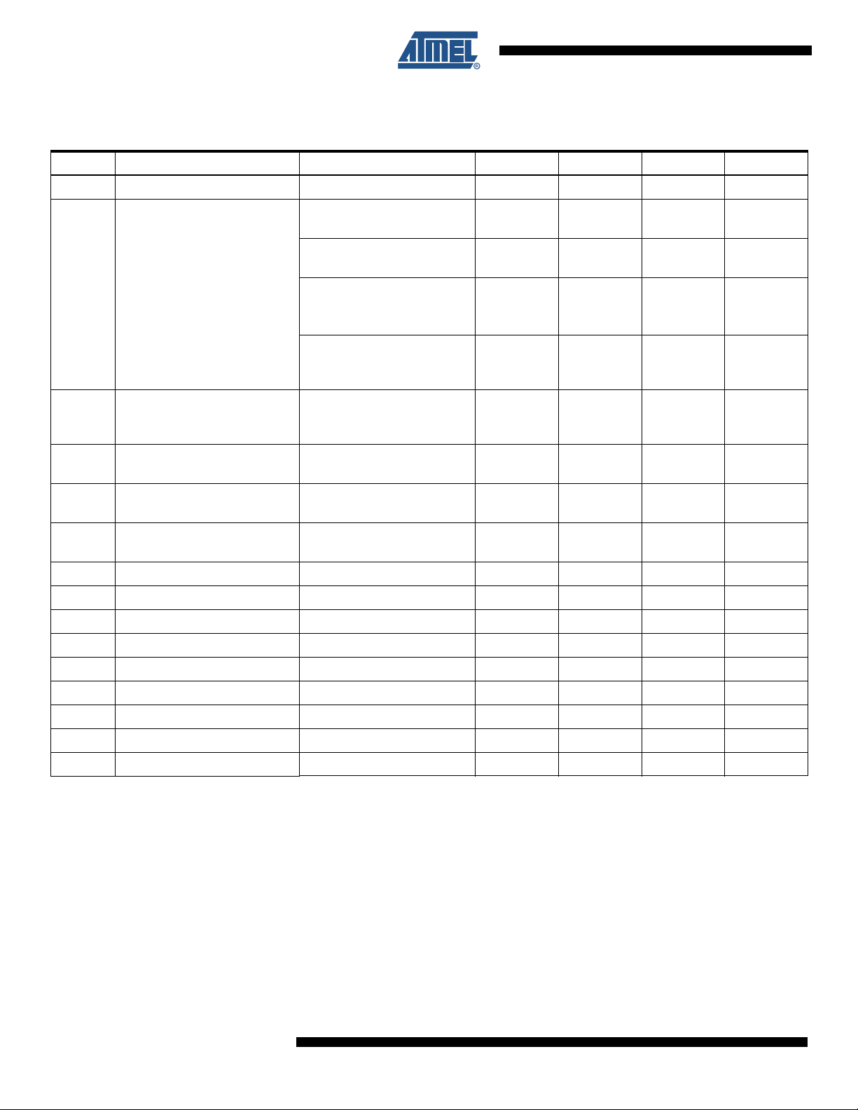
2.7 ADC Characteristics
Table 2-5. ADC Characteristics, Single Ended Channels. T = -40°C to +105°C
Symbol Parameter Condition Min Typ Max Units
Resolution 10 Bits
= 4V, VCC = 4V,
V
Absolute accuracy
(Including INL, DNL, and
Quantization, Gain and Offset
Errors)
Integral Non-Linearity (INL)
(Accuracy after Offset and
Gain Calibration)
Differential Non-linearity
(DNL)
Gain Error
REF
ADC clock = 200 kHz
= 4V, VCC = 4V,
V
REF
ADC clock = 1 MHz
= 4V, VCC = 4V,
V
REF
ADC clock = 200 kHz
Noise Reduction Mode
= 4V, VCC = 4V,
V
REF
ADC clock = 1 MHz
Noise Reduction Mode
= 4V, VCC = 4V,
V
REF
ADC clock = 200 kHz
V
= 4V, VCC = 4V,
REF
ADC clock = 200 kHz
= 4V, VCC = 4V,
V
REF
ADC clock = 200 kHz
2.0 LSB
2.5 LSB
1.5 LSB
2.0 LSB
1.0 LSB
0.5 LSB
2.0 LSB
V
= 4V, VCC = 4V,
Offset Error (Absolute)
REF
ADC clock = 200 kHz
1.5 LSB
Conversion Time Free Running Conversion 14 280 µs
Clock Frequency 50 1000 kHz
V
IN
Input Voltage GND V
REF
V
Input Bandwidth 38.5 kHz
A
REF
V
INT
R
REF
R
AIN
External Voltage Reference 2.0 V
CC
V
Internal Voltage Reference 1.0 1.1 1.2 V
Reference Input Resistance 32 kΩ
Analog Input Resistance 100 MΩ
ADC Conversion Output 0 1023 LSB
6
ATtiny24A/44A
8183D-Appendix A–AVR–08/11
ATtiny24A/44A
Table 2-6. ADC Characteristics, Differential Channels (Unipolar Mode), TA = -40°C to +105°C
Symbol Parameter Condition Min Typ Max Units
Resolution
Absolute accuracy
(Including INL, DNL, and Quantization, Gain
and Offset Errors)
Integral Non-Linearity (INL)
(Accuracy after Offset and Gain Calibration)
Gain Error
Offset Error
Conversion Time Free Running Conversion 70 280 µs
Clock Frequency 50 200 kHz
Gain = 1x 10 Bits
Gain = 20x 10 Bits
Gain = 1x
V
= 4V, VCC = 5V
REF
10 LSB
ADC clock = 50 - 200 kHz
Gain = 20x
= 4V, VCC = 5V
V
REF
15 LSB
ADC clock = 50 - 200 kHz
Gain = 1x
= 4V, VCC = 5V
V
REF
4LSB
ADC clock = 50 - 200 kHz
Gain = 20x
= 4V, VCC = 5V
V
REF
10 LSB
ADC clock = 50 - 200 kHz
Gain = 1x 10 LSB
Gain = 20x 15 LSB
Gain = 1x
V
= 4V, VCC = 5V
REF
3LSB
ADC clock = 50 - 200 kHz
Gain = 20x
V
= 4V, VCC = 5V
REF
4LSB
ADC clock = 50 - 200 kHz
V
V
IN
DIFF
Input Voltage GND V
Input Differential Voltage V
Input Bandwidth 4kHz
A
REF
V
INT
R
REF
R
AIN
External Reference Voltage 2.0 V
Internal Voltage Reference 1.0 1.1 1.2 V
Reference Input Resistance 32 kΩ
Analog Input Resistance 100 MΩ
ADC Conversion Output 0 1023 LSB
8183D-Appendix A–AVR–08/11
CC
/Gain V
REF
- 1.0 V
CC
V
7
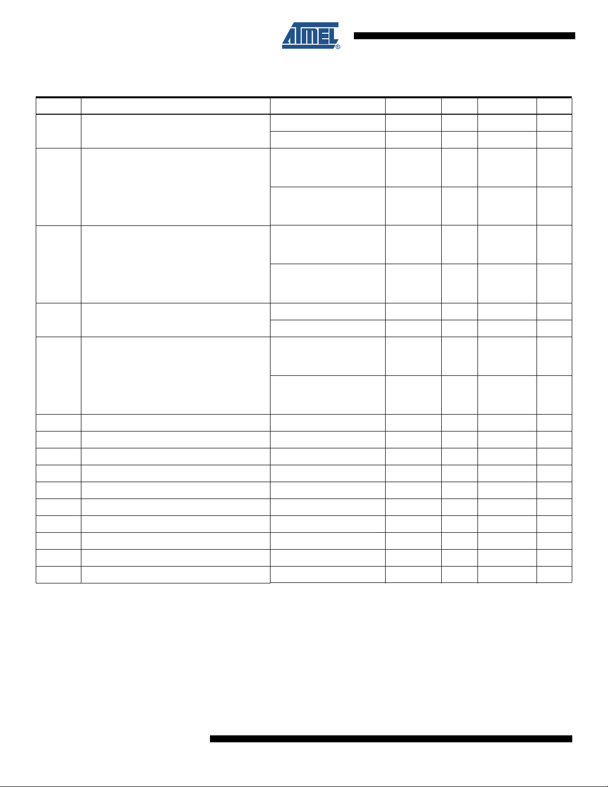
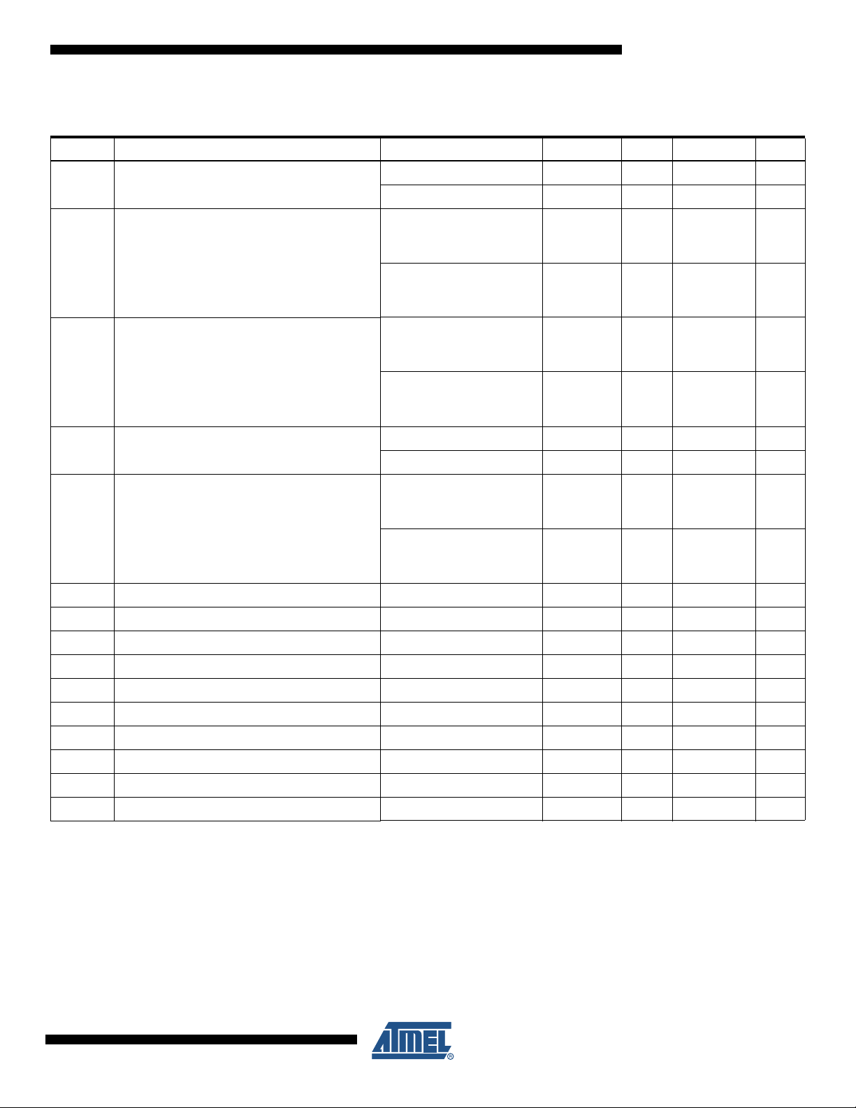
Table 2-7. ADC Characteristics, Differential Channels (Bipolar Mode), TA = -40°C to +105°C
Symbol Parameter Condition Min Typ Max Units
Resolution
Absolute accuracy
(Including INL, DNL, and Quantization, Gain
and Offset Errors)
Integral Non-Linearity (INL)
(Accuracy after Offset and Gain Calibration)
Gain Error
Offset Error
Conversion Time Free Running Conversion 70 280 µs
Clock Frequency 50 200 kHz
Gain = 1x 10 Bits
Gain = 20x 10 Bits
Gain = 1x
V
= 4V, VCC = 5V
REF
8LSB
ADC clock = 50 - 200 kHz
Gain = 20x
= 4V, VCC = 5V
V
REF
8LSB
ADC clock = 50 - 200 kHz
Gain = 1x
= 4V, VCC = 5V
V
REF
4LSB
ADC clock = 50 - 200 kHz
Gain = 20x
= 4V, VCC = 5V
V
REF
5LSB
ADC clock = 50 - 200 kHz
Gain = 1x 4 LSB
Gain = 20x 5 LSB
Gain = 1x
V
= 4V, VCC = 5V
REF
3LSB
ADC clock = 50 - 200 kHz
Gain = 20x
V
= 4V, VCC = 5V
REF
4LSB
ADC clock = 50 - 200 kHz
V
V
IN
DIFF
Input Voltage GND V
Input Differential Voltage V
REF
CC
/Gain V
V
Input Bandwidth 4kHz
A
REF
V
INT
R
REF
R
AIN
External Reference Voltage 2.0 V
- 1.0 V
CC
Internal Voltage Reference 1.0 1.1 1.2 V
Reference Input Resistance 32 kΩ
Analog Input Resistance 100 MΩ
ADC Conversion Output -512 511 LSB
8
ATtiny24A/44A
8183D-Appendix A–AVR–08/11

2.8 Serial Programming Characteristics
Table 2-8. Serial Programming Characteristics, TA = -40°C to +105°C, VCC = 1.8 - 5.5V
(Unless Otherwise Noted)
Symbol Parameter Min Typ Max Units
ATtiny24A/44A
1/t
CLCL
t
CLCL
1/t
CLCL
t
CLCL
t
SHSL
t
SLSH
t
OVSH
t
SHOX
Note: 1. 2 t
Oscillator Frequency 0 4 MHz
Oscillator Period 250 ns
Oscillator Frequency (VCC = 4.5V - 5.5V) 0 20 MHz
Oscillator Period (VCC = 4.5V - 5.5V) 50 ns
SCK Pulse Width High 2 t
SCK Pulse Width Low 2 t
MOSI Setup to SCK High t
MOSI Hold after SCK High 2 t
for fck < 12 MHz, 3 t
CLCL
for fck >= 12 MHz
CLCL
CLCL
CLCL
CLCL
CLCL
(1)
(1)
ns
ns
ns
ns
8183D-Appendix A–AVR–08/11
9
3. Typical Characteristics
105 °C
85 °C
25 °C
-40 °C
0
1
2
3
4
5
6
1.5 2 2.5 3 3.5 4 4.5 5 5.5
V
CC
(V)
I
CC
(mA)
105 °C
85 °C
25 °C
-40 °C
0
0.2
0.4
0.6
0.8
1
1.2
1.5 2 2.5 3 3.5 4 4.5 5 5.5
V
CC
(V)
I
CC
(mA)
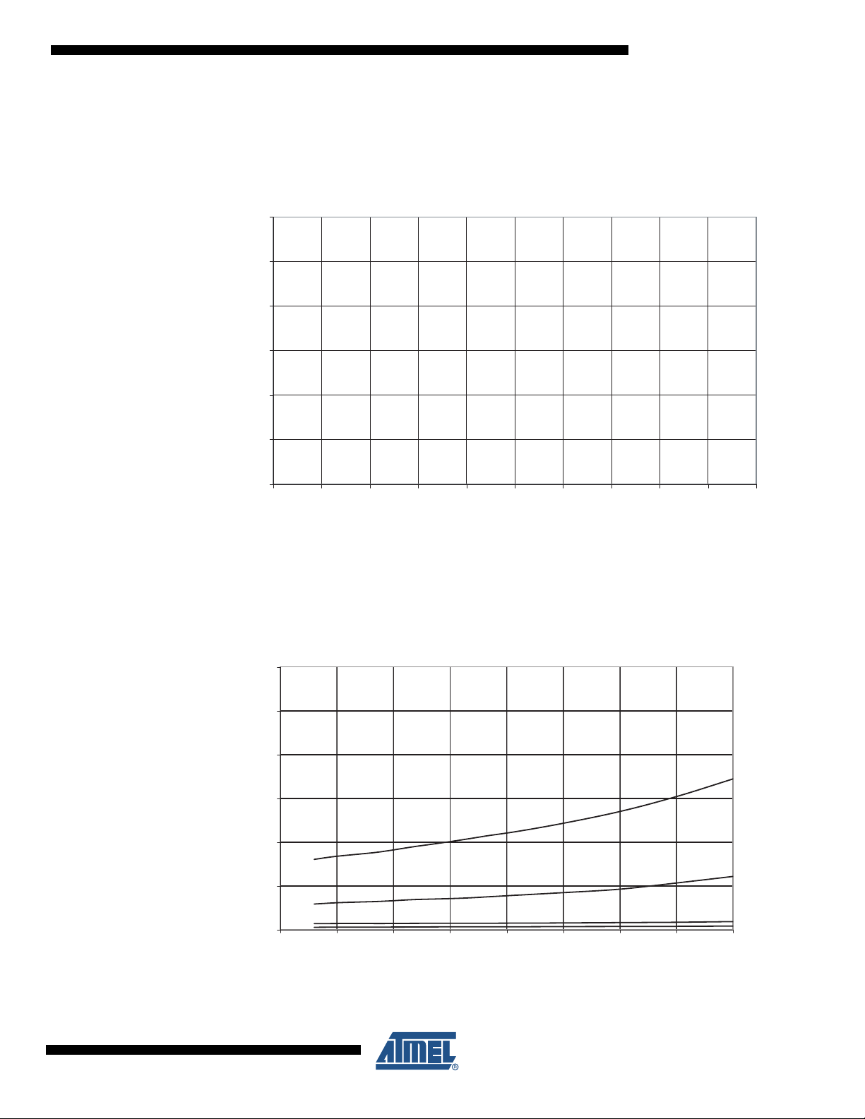
3.1 ATtiny24A
3.1.1 Current Consumption in Active Mode
Figure 3-1. Active Supply Current vs. V
(Internal RC Oscillator, 8 MHz)
CC
Figure 3-2. Active Supply Current vs. V
(Internal RC Oscillator, 1 MHz)
CC
10
ATtiny24A/44A
8183D-Appendix A–AVR–08/11

ATtiny24A/44A
105 °C
85 °C
25 °C
-40 °C
0
0.02
0.04
0.06
0.08
0.1
0.12
0.14
1.5 2 2.5 3 3.5 4 4.5 5 5.5
V
CC
(V)
I
CC
(mA)
105 °C
85 °C
25 °C
-40 °C
0
0.2
0.4
0.6
0.8
1
1.2
1.4
1.6
1.8
2
1.5 2 2.5 3 3.5 4 4.5 5 5.5
V
CC
(V)
I
CC
(mA)
Figure 3-3. Active Supply Current vs. VCC (Internal RC Oscillator, 128 kHz)
3.1.2 Current Consumption in Idle Mode
Figure 3-4. Idle Supply Current vs. V
(Internal RC Oscillator, 8 MHz)
CC
8183D-Appendix A–AVR–08/11
11

Figure 3-5. Idle Supply Current vs. VCC (Internal RC Oscillator, 1 MHz)
105 °C
85 °C
25 °C
-40 °C
0
0.05
0.1
0.15
0.2
0.25
0.3
0.35
0.4
1.5 2 2.5 3 3.5 4 4.5 5 5.5
V
CC
(V)
I
CC
(mA)
105 °C
85 °C
25 °C
-40 °C
0
0.005
0.01
0.015
0.02
0.025
0.03
1.5 2 2.5 3 3.5 4 4.5 5 5.5
V
CC
(V)
I
CC
(mA)
Figure 3-6. Idle Supply Current vs. V
(Internal RC Oscillator, 128 kHz)
CC
12
ATtiny24A/44A
8183D-Appendix A–AVR–08/11
3.1.3 Current Consumption of Standby Supply
TBD
105 °C
85 °C
25 °C
-40 °C
0
0.5
1
1.5
2
2.5
3
1.5 2 2.5 3 3.5 4 4.5 5 5.5
V
CC
(V)
I
CC
(uA)
ATtiny24A/44A
Figure 3-7. Standby Supply Current vs. V
Watchdog Timer Disabled)
(4 MHz External Crystal, External Capacitors,
CC
3.1.4 Current Consumption in Power-down Mode
Figure 3-8. Power-down Supply Current vs. V
(Watchdog Timer Disabled)
CC
8183D-Appendix A–AVR–08/11
13
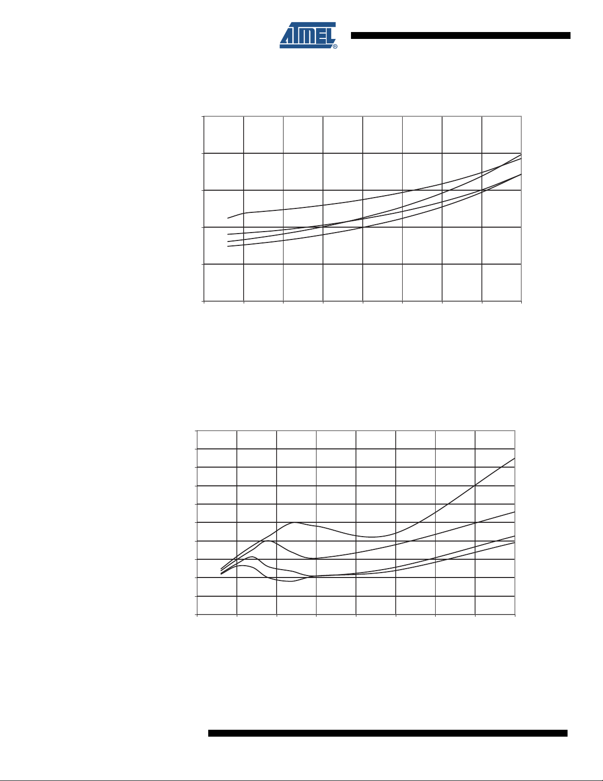
Figure 3-9. Power-down Supply Current vs. VCC (Watchdog Timer Enabled)
105 °C
85 °C
25 °C
-40 °C
0
2
4
6
8
10
1.5 2 2.5 3 3.5 4 4.5 5 5.5
V
CC
(V)
I
CC
(uA)
105 °C
85 °C
25 °C
-40 °C
0
1000
2000
3000
4000
5000
6000
7000
8000
9000
10000
1.5 2 2.5 3 3.5 4 4.5 5 5.5
V
CC
(V)
I
CC
(uA)
3.1.5 Current Consumption of Peripheral Units
Figure 3-10. Programming Current vs. V
CC
14
ATtiny24A/44A
8183D-Appendix A–AVR–08/11

ATtiny24A/44A
105 °C
85 °C
25 °C
-40 °C
0
10
20
30
40
50
1.5 2 2.5 3 3.5 4 4.5 5 5.5
V
CC
(V)
I
CC
(uA)
105 °C
85 °C
25 °C
-40 °C
0
1
2
3
4
5
6
7
8
1.5 2 2.5 3 3.5 4 4.5 5 5.5
V
CC
(V)
I
CC
(uA)
Figure 3-11. Brownout Detector Current vs. VCC (BOD Level = 1.8V)
Figure 3-12. Watchdog Timer Current vs. V
CC
8183D-Appendix A–AVR–08/11
15
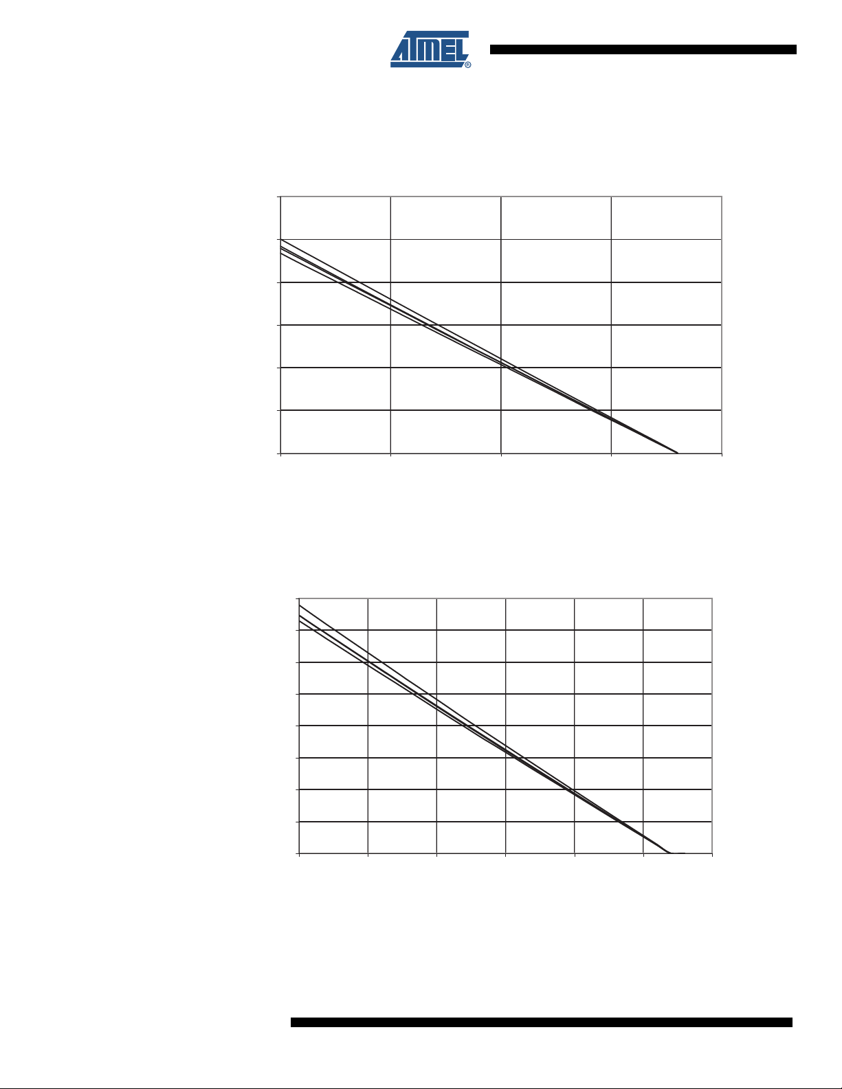
3.1.6 Pull-up Resistors
105 °C
85 °C
25 °C
0
10
20
30
40
50
60
0 0.5 1 1.5 2
V
OP
(V)
I
OP
(uA)
-40 °C
85 °C
25 °C
0
10
20
30
40
50
60
70
80
0 0.5 1 1.5 2 2.5 3
V
OP
(V)
I
OP
(uA)
105 °C
-40 °C
Figure 3-13. Pull-up Resistor Current vs. Input Voltage (I/O Pin, V
= 1.8V)
CC
Figure 3-14. Pull-up Resistor Current vs. input Voltage (I/O Pin, V
16
ATtiny24A/44A
= 2.7V)
CC
8183D-Appendix A–AVR–08/11
ATtiny24A/44A
85 °C
25 °C
0
20
40
60
80
100
120
140
160
012345
V
OP
(V)
I
OP
(uA)
105 °C
-40 °C
105 °C
85 °C
25 °C
-40 °C
0
5
10
15
20
25
30
35
40
0 0,2 0,4 0,6 0,8 1 1,2 1,4 1,6 1,8 2
V
RESET
(V)
I
RESET
(uA)
Figure 3-15. Pull-up Resistor Current vs. Input Voltage (I/O Pin, VCC = 5V)
Figure 3-16. Reset Pull-up Resistor Current vs. Reset Pin Voltage (V
= 1.8V)
CC
8183D-Appendix A–AVR–08/11
17

Figure 3-17. Reset Pull-up Resistor Current vs. Reset Pin Voltage (VCC = 2.7V)
105 °C
85 °C
25 °C
-40 °C
0
10
20
30
40
50
60
35,225,115,00
V
RESET
(V)
I
RESET
(uA)
105 °C
85 °C
25 °C
-40 °C
0
20
40
60
80
100
120
6543210
V
RESET
(V)
I
RESET
(uA)
Figure 3-18. Reset Pull-up Resistor Current vs. Reset Pin Voltage (V
CC
= 5V)
18
ATtiny24A/44A
8183D-Appendix A–AVR–08/11
 Loading...