

Page 1

BDTIC www.bdtic.com/ATMEL
Features
• High Performance, Low Power AVR
• Advanced RISC Architecture
– 123 Powerful Instructions – Most Single Clock Cycle Execution
– 32 x 8 General Purpose Working Registers
– Fully Static Operation
• Non-volatile Program and Data Memories
– 16K Byte of In-System Programmable (ISP) Program Memory Flash
Endurance: 10,000 Write/Erase Cycles
– 512 Bytes In-System Programmable EEPROM
Endurance: 100,000 Write/Erase Cycles
– 512 Bytes Internal SRAM
– Programming Lock for Self-Programming Flash Program and EEPROM Data
Security
– Low size LIN/UART Software In-System Programmable
• Peripheral Features
– LIN 2.1 and 1.3 Controller or 8-Bit UART
– 8-bit Asynchronous Timer/Counter0:
. 10-bit Clock Prescaler
. 1 Output Compare or 8-bit PWM Channel
– 16-bit Synchronous Timer/Counter1:
. 10-bit Clock Prescaler
. External Event Counter
. 2 Output Compares Units or 16-bit PWM Channels on 2x 4 Separated Pins
– Master/Slave SPI Serial Interface,
– Universal Serial Interface (USI) with Start Condition Detector (Master/Slave SPI,
TWI, AES, ...)
– 10-bit ADC:
. 11 Single Ended Channels
. 16 Differential ADC Channel Pairs with Programmable Gain (8x or 20x)
– On-chip Analog Comparator with Selectable Voltage Referenc e
– 100µA ±6% Current Source (LIN Node Identification)
– On-chip Temperature Sensor
– Programmable Watchdog Timer with Separate On-chip Oscillator
• Special Microcontroller Features
– Dynamic Clock Switching (External/Internal RC/Watchdog Clock)
– DebugWIRE On-chip Debug (OCD) System
– Hardware In-System Programmable (ISP) via SPI Port
– External and Internal Interrupt Sources
– Interrupt and Wa ke -up on Pin Change
– Low Power Idle, ADC Noise Reduction, and Power-down Modes
– Enhanced Power-on Reset Circuit
– Programmable Brown-out Detection Circuit
– Internal Calibrated RC Oscillator 8MHz
– 4-16 MHz and 32 KHz Crystal/Ceramic Resonator Oscillators
• I/O and Packages
– 16 Programmable I/O Lines
– 20-pin SOIC, 32-pad QFN and 20 -p in TSSOP
• Operating Voltage:
– 2.7 - 5.5V for ATtiny167
• Speed Grade:
– 0 - 8 MHz @ 2.7 - 5.5V (Automotive Temp. Range: -40°C to +125°C)
– 0 - 16 MHz @ 4.5 - 5.5V (Automotive Temp. Range: -40°C to +125°C)
®
8-Bit Microcontroller
8-bit
Microcontroller
with 16K Bytes
In-System
Programmable
Flash
and
LIN Controller
ATtiny167
Automotive
Preliminary
7728A-AUTO-07/08
Page 2

1. Description
1.1 Part Description
The ATtiny167 is a low-power CMOS 8-bit microcontroller based on the AVR enhanced RISC
architecture. By executing powerful instructions in a single clock cycle, the ATtiny167 achieves
throughputs approaching 1 MIPS pe r MHz allow ing the sy stem de signer to op timize po wer con sumption versus processing speed.
The AVR core combines a rich instruction set with 32 general purpose working registers. All the
32 registers are directly connected to the Arithmetic Logic Unit (ALU), allowing two independent
registers to be accessed in one single instruction executed in one clock cycle. The resulting
architecture is more code efficient while achieving throughputs up to ten times faster than conventional CISC microcontrollers.
The ATtiny167 provides the following features: 16K byte of In-System Programmable Flash, 512
bytes EEPROM, 512 bytes SRAM, 6 general purpose I/O lines, 32 general purpose working registers, one 8-bit Timer/Counter with compare modes, one 8-bit high speed Timer/Co unter,
Universal Serial Interface, a LIN controller, Internal and External Interrupts, a 4-channel, 10-bit
ADC, a programmable Watchdog Timer with internal Oscillator, and three software selectable
power saving modes. The Idle mode stops the CPU while allowing the SRAM, Timer/Counter,
ADC, Analog Comparator, an d Inte rrup t syst em t o co ntinu e fu nctio ning. Th e Pow er-dow n mode
saves the register contents, disabling all chip functions until the nex t Interrupt or Hardware
Reset. The ADC Noise Reduction mode stops the CPU and all I/O modules except ADC, to minimize switching noise during ADC conversions.
The device is manufactured using Atmel’s high density non-volatile memory technology. The
On-chip ISP Flash allows the Program memory to be re-programmed In-System through an SPI
serial interface, by a conventional non-volatile memory programmer or by an On-chip boot code
running on the AVR core. The Boot program can use any interface to download the application
program in the Flash memory. By combining an 8-bit RISC CPU with In-System Self-Programmable Flash on a monolithic chip, the Atmel ATtin y167 is a powerful microcontroller that
provides a highly flexible and cost effective solution to many embedded control applications.
The ATtiny167 AVR is supported w ith a full suite of program and system development tools
including: C Compilers, Macro Assemblers, Program Debugger/Simulators, In-Circuit Emulators,
and Evaluation kits.
1.2 Automotive Quality Grade
The ATtiny167 have been developed and manufactured according to the most stringent requirements of the international standard ISO-TS-16949. This data sheet contains limit values
extracted from the results of exten sive characterizatio n (temperature and voltage). The q uality
and reliability of the ATtiny167 have been verified during regular product qualification as per
AEC-Q100 grade 1.
As indicated in the ordering information paragraph, the products are available in only one temperature grade as listed in Table 1-1.
Table 1-1. Temperature Grade Identification for Automotive Products
Temperature
-40°C / +125°C Z Automotive Temperature Range
Temperature
Identifier
Comments
2
ATtiny167
7728A–AUTO–07/08
Page 3
1.3 Disclaimer
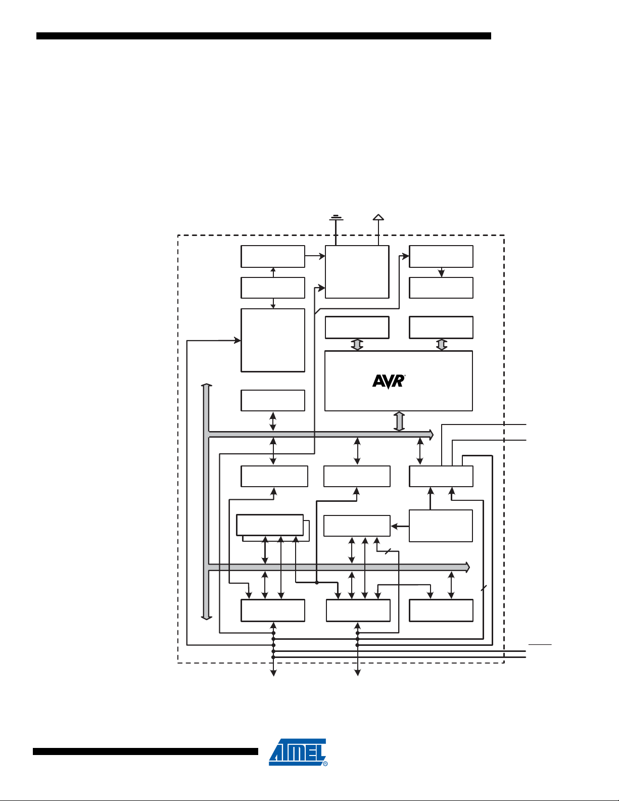
PORT A (8) LIN / UARTPORT B (8)
SPI & USI
Timer/Counter-0
Timer/Counter-1 A/D Conv.
Internal
Voltage
References
Analog Comp.
SRAMFlash
EEPROM
Watchdog
Oscillator
Watchdog
Timer
Oscillator
Circuits /
Clock
Generation
Powe r
Supervision
POR / BOD &
RESET
VCC
GND
PROGRAM
LOGIC
debugWIRE
AGND
AVCC
DATA B U S
PA[0..7]PB[0..7]
11
RESET
XTAL[1;2]
CPU
2
1.4 Block Diagram
ATtiny167
Typical values contained in this data sheet are based on simulations and characterization of
other AVR microcontrollers manufactured on the same process technology. Min. and Max
values will be available after the device is characterized.
Figure 1-1. Block Dia gram
7728A–AUTO–07/08
3
Page 4

1.5 Pin Configuration
PB0 (PCINT8 / OC1AU / DI / SDA)
PB1 (PCINT9 / OC1BU / DO)
PB2 (PCINT10 / OC1AV / USCK / SCL)
PB3 (PCINT11 / OC1BV)
GND
VCC
PB4 (PCINT12 / OC1AW / XTAL1 / CLKI)
PB5 (PCINT13 / ADC8 / OC1BW / XTAL2 / CLKO)
PB6 (PCINT14 / ADC9 / OC1AX / INT0)
PB7 (PCINT15 / ADC10 / OC1BX / RESET / dW)
(RXLIN / RXD / ADC0 / PCINT0) PA0
(TXLIN / TXD / ADC1 / PCINT1) PA1
(MISO / DO / OC0A / ADC2 / PCINT2) PA2
(INT1 / ISRC / ADC3 / PCINT3) PA3
AVCC
AGND
(MOSI / SDA / DI / ICP1 / ADC4 / PCINT4) PA4
(SCK / SCL / USCK / T1 / ADC5 / PCINT5) PA5
(SS / AIN0 / ADC6 / PCINT6) PA6
(AREF / XREF / AIN1 / ADC7 / PCINT7) PA7
1
2
3
4
5
6
7
8
9
10
20
19
18
17
16
15
14
13
12
11
20-pin
top
view
(INT0 / OC1AX / ADC9 / PCINT14 ) PB6
PB5 (PCINT13 / ADC8 / OC1BW / XTAL2 / CLKO)
PB4 (PCINT12 / OC1AW / XTAL1 / CLKI)
VCC
GND
1
2
3
4
5
21
20
19
18
17
323029
28
31
9
11
12
13
10
32-lead
top view
PB2 (PCINT10 / OC1AV / USCK / SCL)
PB1 (PCINT9 / OC1BU / DO) (dW / RESET / OC1BX / ADC10 / PCINT15) PB7
(AREF / XREF / AIN1 / ADC7 / PCINT7) PA7
(SS / AIN0 / ADC6 / PCINT6) PA6
(SCK / SCL / USCK / T1 / ADC5 / PCINT5) PA5
AGND
AVCC
(INT1 / ISRC / ADC3 / PCINT3) PA3
PA1 (PCINT1 / ADC1 / TXD / TXLIN)
PA2 (PCINT2 / ADC2 / OC0A / DO / MISO)
nc
nc
nc
nc
nc
nc
nc
nc
nc
nc
nc nc
PA0 (PCINT0 / ADC0 / RXD / RXLIN)
INDEX CORNER
Bottom pad should be
soldered to ground
6
7
8
141516
PB3 (PCINT11 / OC1BV)
24
23
22
272526
PB0 (PCINT8 / OC1AU / DI / SDA)
(MOSI / SDA / DI / ICP1 / ADC4 / PCINT4) PA4
Figure 1-2. Pinout ATtiny167 - SOIC20 & TSSOP20
Figure 1-3. Pinou t ATt iny 16 7 - QF N3 2
1.6 Pin Description
1.6.1 Vcc
4
ATtiny167
Supply voltage.
7728A–AUTO–07/08
Page 5

1.6.2 GND
Ground.
1.6.3 AVcc
Analog supply voltage.
1.6.4 AGND
Analog ground.
1.6.5 Port A (PA7..PA0)
Port A is an 8-bit bi-directional I/O port wit h intern al pull-up r esistors ( selecte d for each bit). The
Port A output buffers have symmetrical drive characteristics with both high sink and source
capability. As inputs, Port A pins that are externally pulled low will source current if the pull-up
resistors are activated. The Port A pins are tri-stated when a reset co ndition becomes active,
even if the clock is not running.
Port A also serves the functions of various special feat ures of the AT tiny167 as liste d on Section
9.3.3 ”Alternate Functions of Port A” on page 73.
1.6.6 Port B (PB7..PB0)
Port B is an 8-bit bi-directional I/O port wit h intern al pull-up r esistors ( selecte d for each bit). The
Port B output buffers have symmetrical drive characteristics with both high sink and source
capability. As inputs, Port B pins that are externally pulled low will source current if the pull-up
resistors are activated. The Port B pins are tri-stated when a reset co ndition becomes active,
even if the clock is not running.
ATtiny167
Port B also serves the functions of various special feat ures of the AT tiny167 as liste d on Section
9.3.4 ”Alternate Functions of Port B” on page 78.
1.7 Resources
A comprehensive set of development tools, application notes and datasheets are available for
download on http://www.atmel.com/avr.
1.8 About Code Examples
This documentation contains simple code examples that briefly sh ow how to use vari ous parts of
the device. These code examples assume that the part specific header file is included b efore
compilation. Be aware that not all C compiler vendors include bit definitions in the header files
and interrupt handling in C is compiler dependent. Plea se con firm with th e C com piler d ocumentation for more details.
7728A–AUTO–07/08
5
Page 6
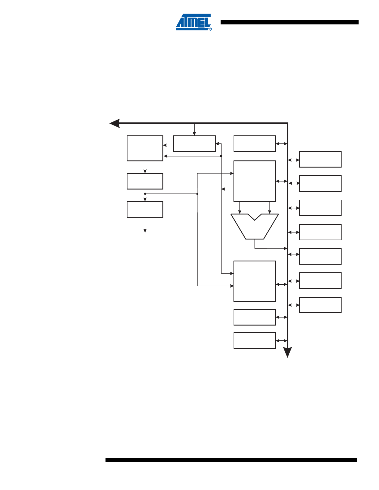
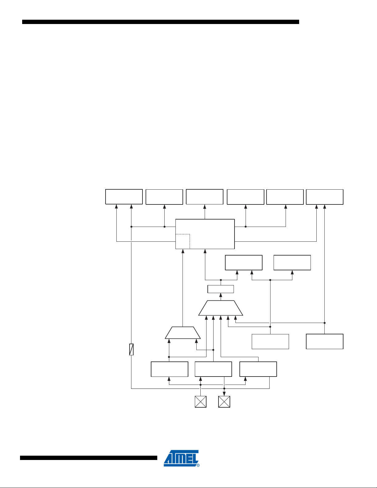
2. AVR CPU Core
Flash
Program
Memory
Instruction
Register
Instruction
Decoder
Program
Counter
Control Lines
32 x 8
General
Purpose
Registrers
ALU
Status
and Control
EEPROM
Data Bus 8-bit
I/O Lines
Data
SRAM
Direct Addressing
Indirect Addressing
I/O Module 2
Analog
Comparator
I/O Module1
Watchdog
Timer
I/O Module n
Interrupt
Unit
A.D.C.
2.1 Overview
This section discusses the AVR core architecture in general. The main function of the CPU core
is to ensure correct program execution. The CPU must therefore be able to access memories,
perform calculations, control peripherals, and handle interrupts.
Figure 2-1. Block Diagram of the AVR Architecture
In order to maximize performance and parallelism, the AVR uses a Harvard architecture – with
separate memories and buses for program and data. Instructions in the Program memory are
executed with a single level pipe lining. While one instruc tion is being executed, the next instruction is pre-fetched from the Program memory. This concept enables instructions to be executed
in every clock cycle. The Program memory is In-System Reprogrammable Flash memory.
The fast-access Register File contains 32 x 8-bit general purpose working registers with a single
clock cycle access time. This allows single-cycle Arithmetic Logic Unit (ALU) opera tion. In a
typical ALU operation, two operands are output from the Reg ister File, the opera tion is executed,
and the result is stored back in the Register File – in one clock cycle.
6
ATtiny167
7728A–AUTO–07/08
Page 7

ATtiny167
Six of the 32 registers can be used as three 16-bit indirect address register pointers for Data
Space addressing – enabling efficient address calculations. One of the these address pointers
can also be used as an address pointer for look up tables in Flash Program memory. These
added function registers are the 16-bit X-, Y-, and Z-register, described later in this section.
The ALU supports arithmetic and logic operations between registers or between a constant and
a register. Single register operations can also be executed in the ALU. After an arithmetic operation, the Status Register is updated to reflect information about the result of the operation.
Program flow is provided by conditional and unconditional jump and call instructions, able to
directly address the whole address space. Most AVR instructions have a single 16-bit word
format. Every Program memory address contains a 16- or 32-bit instruction.
During interrupts and subroutine calls, the return address Program Counter (PC) is stored on the
Stack. The Stack is effectively allocated in the general data SRAM, and consequently the Stack
size is only limited by the total SRAM size and the usage of the SRAM. All user programs must
initialize the SP in the Reset routine (before subroutines or interrupts are executed). The Stack
Pointer (SP) is read/write accessible in the I/O space. The data SRAM can easily be accessed
through the five different addressing modes supported in the AVR architecture.
The memory spaces in the AVR architecture are all linear and regular memory maps.
A flexible interrupt module has its control registers in the I/O space with an additional Global
Interrupt Enable bit in the Status Register. All interrupts have a separate Interrupt Vector in the
Interrupt Vector table. The interrupts have priority in accordance with their Interrupt Vector position. The lower the Interrupt Vector address, the higher the priority.
The I/O memory space contains 64 addresses for CPU peripheral functions as Control Registers, SPI, and other I/O functions. The I/O memory can be acces sed directly, or as the Data
Space locations following those of the Register File, 0x20 - 0x5F.
2.2 ALU – Arithmetic Logic Unit
The high-performance AVR ALU operates in direct connection with all the 32 general purpose
working registers. Within a single clock cycle, arithmetic operations between general purpose
registers or between a register and an immediate are executed. The ALU opera tions are divided
into three main categories – arithmetic, logical, and bit-functions. Some implementations of the
architecture also provide a powerful multiplier supporting both signed/unsigned multiplication
and fractional format. See the “Instruction Set” section for a detailed description.
2.3 Status Register
The Status Register contains information about the result of the most recently executed arithmetic instruction. This information can be used for altering program flow in order to perform
conditional operations. Note that the Status Register is updated after all ALU operations, as
specified in the Instruction Set Reference. This will in man y case s re move th e need for using the
dedicated compare instructions, resulting in faster and more compact code.
The Status Register is not automatically stored when entering an interrupt routine and restored
when returning from an interrupt. This must be ha nd le d by software.
7728A–AUTO–07/08
7
Page 8

2.3.1 SREG – AVR Status Register
The AVR Status Register – SREG – is defined as:
Bit 76543210
Read/Write R/W R/W R/W R/W R/W R/W R/W R/W
Initial Value00000000
• Bit 7 – I: Global Interrupt Enable
The Global Interrupt Enable bit must be set for the interrupts to be enabled. The individual interrupt enable control is then performed in separate control registers. If the Global Interrupt Enable
Register is cleared, none of the interrupts are enabled independent of the individual interrupt
enable settings. The I-bit is cleared by hardware after an interrupt has occurred, and is set by
the RETI instruction to enable subsequent interrupts. The I-bit can also be set and cleared by
the application with the SEI and CLI instructions, as described in the instruction set reference.
• Bit 6 – T: Bit Copy Storage
The Bit Copy instructions BLD (Bit LoaD) and BST (Bit STore) use the T-bit as source or destination for the operated bit. A bit from a register in the Register File can be copied into T by the
BST instruction, and a bit in T can be copied into a bit in a register in the Register File by the
BLD instruction.
• Bit 5 – H: Half Carry Flag
The Half Carry Flag H indicates a Half Carry in some arithmetic operations. Half Carry is useful
in BCD arithmetic. See the “Instruction Set Description” for detailed information.
I T H S V N Z C SREG
• Bit 4 – S: Sign Bit, S = N
⊕ V
The S-bit is always an exclusive or between the Negative Flag N and the Two’s Complement
Overflow Flag V. See the “Instruction Set Description” for detailed information.
• Bit 3 – V: Two’s Complement Overflow Flag
The Two’s Complement Overflow Flag V supports two’s complement arithmetics. See the
“Instruction Set Description” for detailed information.
• Bit 2 – N: Negative Flag
The Negative Flag N indicates a negative result in an arithmetic or logic operation. See the
“Instruction Set Description” for detailed information.
• Bit 1 – Z: Zero Flag
The Zero Flag Z indicates a zero result in an arithmetic or logic operation. See the “Instruction
Set Description” for detailed information.
• Bit 0 – C: Carry Flag
The Carry Flag C indicates a carry in an arithmetic or logic operation. See the “Instruction Set
Description” for detailed information.
8
ATtiny167
7728A–AUTO–07/08
Page 9

2.4 General Purpose Register File
The Register File is optimized for the AVR Enhanced RISC instruction set. In order to achieve
the required performance and flexibility, the following input/output schemes are supported by the
Register File:
• One 8-bit output operand and one 8-bit result input
• Two 8-bit output operands and one 8-bit result input
• Two 8-bit output operands and one 16-bit result input
• One 16-bit output operand and one 16-bit result input
Figure 2-2 shows the structure of the 32 general purpose working registers in the CPU.
Figure 2-2. AVR CPU General Purpose Working Registers
General R14 0x0E
Purpose R15 0x0F
Working R16 0x10
Registers R17 0x11
ATtiny167
7 0 Addr.
R0 0x00
R1 0x01
R2 0x02
…
R13 0x0D
…
R26 0x1A X-register Low Byte
R27 0x1B X-register High Byte
R28 0x1C Y-register Low Byte
R29 0x1D Y-register High Byte
R30 0x1E Z-register Low Byte
R31 0x1F Z-register High Byte
Most of the instructions operating on the Register File have direct access to all registers, and
most of them are single cycle instructions.
As shown in Figure 2-2, each register is also assigned a Data memory address, mapping them
directly into the first 32 locations of the user Data Space. Although not being physically implemented as SRAM locations, this memory organization provides great flexibility in access of the
registers, as the X-, Y- and Z-pointer registers can be set to index any register in the file.
2.4.1 The X-register, Y-register, and Z-register
The registers R26..R31 have some a dded functions to their general purpose usage. These registers are 16-bit address pointers for indirect addressing of the data space. The three indirect
address registers X, Y, and Z are defined as described in Figure 2-3 on page 10.
7728A–AUTO–07/08
9
Page 10
2.5 Stack Pointer
Figure 2-3. The X-, Y-, and Z-registers
15 XH XL 0
X-register 7 0 7 0
R27 (0x1B) R26 (0x1A)
15 YH YL 0
Y-register 7 0 7 0
R29 (0x1D) R28 (0x1C)
15 ZH ZL 0
Z-register 7 0 7 0
R31 (0x1F) R30 (0x1E)
In the different addressing modes these address registers have functions as fixed d isplacem ent,
automatic increment, and automatic decrement (see the instruction set reference fo r details).
The Stack is mainly used for storing temporary data, for storing local variables and for storing
return addresses after interrupts and subroutine calls. The Stack Pointer Register always points
to the top of the Stack. Note that the Stack is implemented as growing from higher memor y locations to lower memory locations. This implies that a Stack PUSH command decreases the Stack
Pointer.
The Stack Pointer points to the data SRAM Stack area where the Subroutine and Interrupt
Stacks are located. This Stack space in the data SRAM must be defined by the program before
any subroutine calls are executed or interrupts are enabled. The Stack Pointer must be set to
point above 0x60. The Stack Pointer is decremented by one when data is pushed onto the Stack
with the PUSH instruction, and it is decremented by two when the return address is pushed onto
the Stack with subroutine call or interrupt. The Stack Pointer is incremented by one when data is
popped from the Stack with the POP instruction, and it is incremented by two when data is
popped from the Stack with return from subroutine RET or return from interrupt RETI.
The AVR Stack Pointer is implemented as two 8-bit registers in the I/O space. The number of
bits actually used is implementation dependent. Note that the data space in some implementations of the AVR architecture is so small that only SPL is needed. In this case, the SPH Register
will not be present
2.5.1 SPH and SPL – Stack Pointer Register
Bit 151413121110 9 8
SP15 SP14 SP13 SP12 SP11 SP10 SP9 SP8 SPH
SP7 SP6 SP5 SP4 SP3 SP2 SP1 SP0 SPL
76543210
Read/Write R/W R/W R/W R/W R/W R/W R/W R/W
R/W R/W R/W R/W R/W R/W R/W R/W
Initial Value RAMEND RAMEND RAMEND RAMEND RAMEND RAMEND RAMEND RAMEND
RAMEND RAMEND RAMEND RAMEND RAMEND RAMEND RAMEND RAMEND
10
ATtiny167
7728A–AUTO–07/08
Page 11
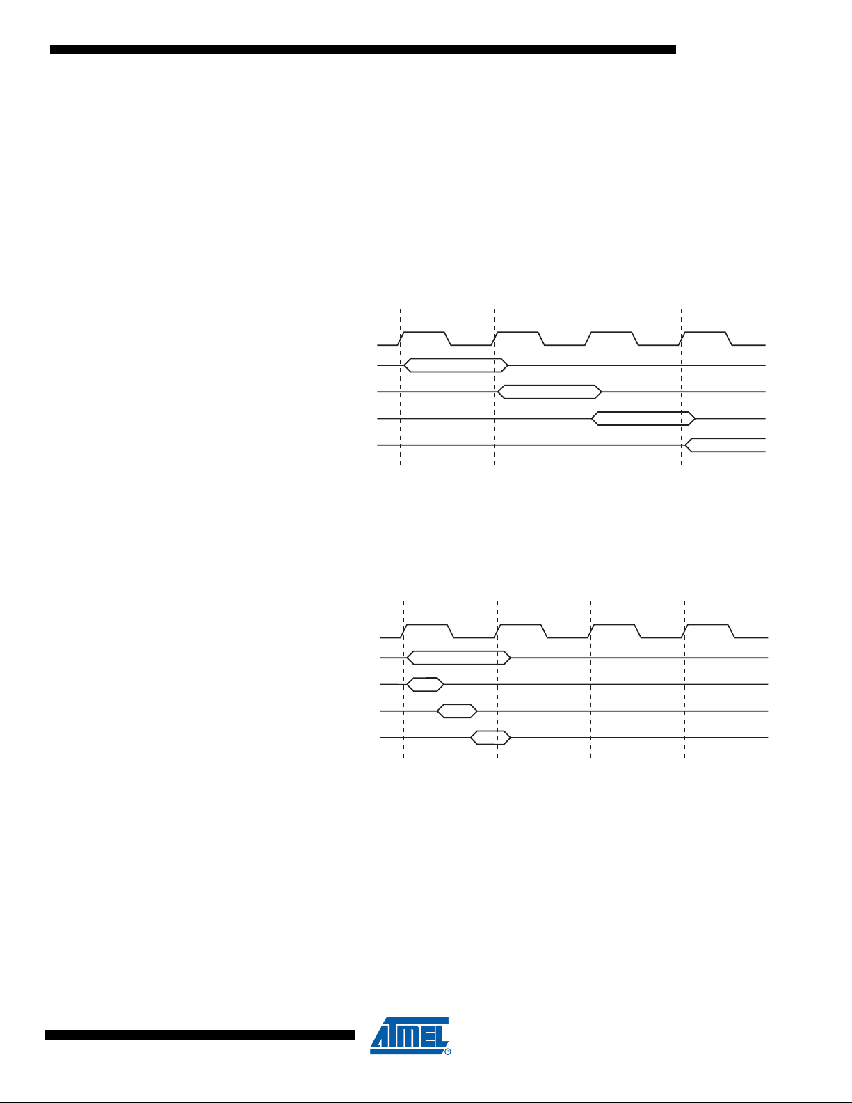
2.6 Instruction Execution Timing
clk
1st Instruction Fetch
1st Instruction Execute
2nd Instruction Fetch
2nd Instruction Execute
3rd Instruction Fetch
3rd Instruction Execute
4th Instruction Fetch
T1 T2 T3 T4
CPU
Total Execution Time
Register Operands Fetch
ALU Operation Execute
Result Write Back
T1 T2 T3 T4
clk
CPU
This section describes the general access timing concepts for instruction execution. The AVR
CPU is driven by the CPU clock clk
chip. No internal clock division is used.
Figure 2-4 shows the parallel instruction fetches and instruction executions enabled by the
Harvard architecture and the fast access Register File concept. This is the basic pipelining
concept to obtain up to 1 MIPS per MHz with the corresponding unique results for functions per
cost, functions per clocks, and functions per power-unit.
Figure 2-4. The Parallel Instruction Fetches and Instruction Executions
ATtiny167
, directly generated from the selected clock source for the
CPU
2.7 Reset and Interrupt Handling
7728A–AUTO–07/08
Figure 2-5 shows the internal timing concept for the Register File. In a single clock cycl e an ALU
operation using two register operands is executed, and the result is stored back to the destination register.
Figure 2-5. Single Cycle ALU Operation
The AVR provides several different interrupt sources. These interrupts and the separate Reset
Vector each have a separate Program Vector in the Program memory space. All interrupts are
assigned individual enable bits which must be written logic one together with th e Global Interrupt
Enable bit in the Status Register in order to enable the interrupt.
The lowest addresses in the Program memory space are by default defined as the Reset and
Interrupt Vectors. The complete list of vectors is shown in Section 7. ”Interrupts” on page 57.
The list also determines the priority levels of the different interrupts. The lower the address the
higher is the priority level. RESET has the highest priority, and next is INT0 – the External Interrupt Request 0.
11
Page 12

2.7.1 Interrupt behavior
When an interrupt occurs, the Global Interrupt Enable I-bit is cleared and all interrupts are disabled. The user software can write logic one to the I-bit to enable nested interrupts. All enabled
interrupts can then interrupt the current interrupt routine. The I-bit is automatically set when a
Return from Interrupt instruction – RETI – is executed.
There are basically two types of interrupts. The first type is triggered by an event that sets the
Interrupt Flag. For these interrupts, the Program Counter is vectored to the actual Interrupt
Vector in order to execute the interrupt handling routine, and hardware clears the corresponding
Interrupt Flag. Interrupt Flags can also be cleared by writing a logic one to the flag bit position(s)
to be cleared. If an interrupt condition occurs while the corresponding interrupt enable bit is
cleared, the Interrupt Flag will be set and remembered until the interrupt is enabled, or the flag is
cleared by software. Similarly, if one or more interrupt conditions occur while the Global Interrupt
Enable bit is cleared, the corresponding Interrupt Flag(s) will be set and remembered until the
Global Interrupt Enable bit is set, and will then be executed by order of priority.
The second type of interrupts will trigger as long as the interrupt condition is present. These
interrupts do not necessarily have Interrupt Flags. If the interrupt condition disap pears befo re the
interrupt is enabled, the interrupt will not be triggered.
When the AVR exits from an interrupt, it will always return to the main program and execute one
more instruction before any pending interrupt is served.
Note that the Status Register is not automatically stored when entering an interrupt routine, nor
restored when returning from an interrupt routine. This must be handled by software.
When using the CLI instruction to disable interrupts, the interrupts will be immediately disabled.
No interrupt will be executed after the CLI instruction, even if it occurs simultaneously with the
CLI instruction. The following example shows how this can be used to avoid interrupts during the
timed EEPROM write sequence.
Assembly Code Example
in r16, SREG ; store SREG value
cli ; disable interrupts during timed sequence
sbi EECR, EEMPE ; start EEPROM write
sbi EECR, EEPE
out SREG, r16 ; restore SREG value (I-bit)
C Code Example
char cSREG;
cSREG = SREG; /* store SREG value */
/* disable interrupts during timed sequence */
_CLI();
EECR |= (1<<EEMPE); /* start EEPROM write */
EECR |= (1<<EEPE);
SREG = cSREG; /* restore SREG value (I-bit) */
12
ATtiny167
7728A–AUTO–07/08
Page 13

When using the SEI instruction to enable interrupts, the instruction following SEI will be executed before any pending interrupts, as shown in this example.
Assembly Code Example
sei ; set Global Interrupt Enable
sleep ; enter sleep, waiting for interrupt
; note: will enter sleep before any pending
; interrupt(s)
C Code Example
_SEI(); /* set Global Interrupt Enable */
_SLEEP(); /* enter sleep, waiting for interrupt */
/* note: will enter sleep before any pending interrupt(s) */
2.7.2 Interrupt Response Time
The interrupt execution response for all the enabled AVR interrupts is four clock cycles minimum. After four clock cycles the Program Vector address for the actual interrupt handling routine
is executed. During this four clock cycle period, the Program Counter is pushed onto the Stack.
The vector is normally a jump to the interrupt routine, and this jump takes three clock cycles. If
an interrupt occurs during execution of a multi-cycle instruction, this instruction is completed
before the interrupt is served. If an interrupt occurs when the MCU is in sleep mode, the interrupt
execution response time is increased by four clo ck cycles. This increase comes in addition to the
start-up time from the selected sleep mode.
ATtiny167
A return from an interrupt handling routine takes four clock cycles. During these four clock
cycles, the Program Counter (two bytes) is popped back from the Stack, the Stack Pointer is
incremented by two, and the I-bit in SREG is set.
7728A–AUTO–07/08
13
Page 14

3. AVR Memories
This section describes the different memories in the ATtiny167. The AVR architecture has two
main memory spaces, the Data memory and the Program memory space. In addition, the
ATtiny167 features an EEPROM Memory for data storage. All three memory spaces are lin ear
and regular.
Table 3-1. Memory Mapping.
Memory Mnemonic ATtiny167
Flash
32 Registers
I/O
Registers
Ext I/O
Registers
Internal
SRAM
EEPROM
Size
Start Address
End Address
Size
Start Address
End Address
Size
Start Address
End Address
Size
Start Address
End Address
Size
Start Address
End Address
Size
Start Address
End Address
Flash size 16 K bytes
-
Flash end
- 32 bytes
- 0x0000
- 0x001F
- 64 bytes
- 0x0020
- 0x005F
- 160 bytes
- 0x0060
- 0x00FF
ISRAM size 512 bytes
ISRAM start 0x0100
ISRAM end 0x02FF
E2 size 512 bytes
- 0x0000
E2 end 0x01FF
0x3FFF
0x1FFF
(1)
(2)
Notes: 1. Byte address.
2. Word (16-bit) address.
3.1 In-System Re-programmable Flash Program Memory
The ATtiny167 contains On-chip In-System Reprogrammable Flash memory for program
storage (see “Flash size” in Table 3-1 on page 14). Since all AVR instructions are 16 or 32 bits
wide, the Flash is organized as 16 bits wide. ATtiny167 does not have separate Boot Lo ader and
Application Program sections, and the SPM instruction can be executed from the entire Flash.
See SELFPRGEN description in Section 20.2.1 ”Store Program Memory Control and Status
Register – SPMCSR” on page 210 for more details.
The Flash memory has an endurance of at least 10,000 write/erase cycles in automotive range.
The ATtiny167 Program Counter (PC) address the program memory locations. Section 21.
”Memory Programming” on page 216 contains a detailed description on Flash data serial down-
loading using the SPI pins.
Constant tables can be allocated within the entire Prog ram memory address space (se e the
LPM – Load Program memory instruction description).
Timing diagrams for instruction fetch and execution are presented in Section 2.6 ”Instruction
Execution Timing” on page 11.
14
ATtiny167
7728A–AUTO–07/08
Page 15

Figure 3-1. Program Memory Map
0x0000
Flash end
Program Memory
3.2 SRAM Data Memory
Figure 3-2 shows how the ATtiny167 SRAM Memory is organized.
ATtiny167
The ATtiny167 is a complex microcontroller with more peripheral units tha n can be supported
within the 64 locations reserved in the Opcode for the IN and OUT instructions. For the
Extended I/O space in SRAM, only the ST/STS/STD and LD/LDS/LDD instructions can be used.
The data memory locations address both the Register File, the I/O memory, Extended I/O
memory, and the internal data SRAM. The first 32 locations address the Register File, the next
64 location the standard I/O memory, then 160 locations of Extended I/O memory, and the next
locations address the internal data SRAM (see “ISRAM size” in Table 3-1 on page 14).
The five different addressing modes for the Data memory cov er: Direct, Indirect with Displacement, Indirect, Indirect with Pre-decrement, and Indirect with Post-increment. In the Register
File, registers R26 to R31 feature the indirect addressing pointer registers.
The direct addressing reaches the entire data space.
The Indirect with Displacement mode reaches 63 address locations from the base addres s given
by the Y- or Z-register.
When using register indirect addressing modes with automatic pre-decrement and post-incre-
ment, the address registers X, Y, and Z are decremented or incremented.
The 32 general purpose working registers, 64 I/O Registers, 160 Extended I/O Registers and the
internal data SRAM in the ATtiny167 are all accessible through all these add ressing mo des. The
Register File is described in ”General Purpose Register File” on page 9.
7728A–AUTO–07/08
15
Page 16
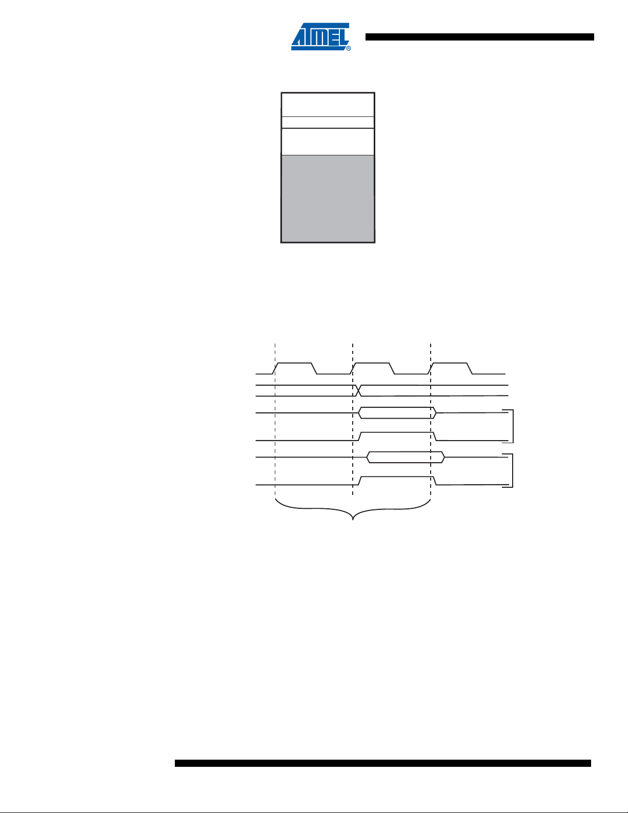
Figure 3-2. Data Memory Map
32 Registers
64 I/O Registers
Internal SRAM
(ISRAM size)
0x0000 - 0x001F
0x0020 - 0x005F
ISRAM end
0x0060 - 0x00FF
Data Memory
160 Ext I/O Reg.
ISRAM start
clk
WR
RD
Data
Data
Address
Address valid
T1 T2 T3
Compute Address
Read
Write
CPU
Memory Access Instruction
Next Instruction
3.2.1 Data Memory Access Times
This section describes the general access timing concepts for internal memory access. The
internal data SRAM access is performed in two clk
Figure 3-3. On-chip Data SRAM Access Cycles
cycles as described in Figure 3-3.
CPU
3.3 EEPROM Data Memory
3.3.1 EEPROM Read/Write Access
16
The ATtiny167 contains EEPROM memory (see “E2 size” in Table 3-1 on page 14). It is organized as a separate data space, in which single bytes can be read and written. The EEPROM
has an endurance of at least 100,000 write/erase cycles in automotive range. The access
between the EEPROM and the CPU is described in the following, specifying the EEPROM
Address Registers, the EEPROM Data Register and the EEPROM Control Register.
Section 21. ”Memory Programming” on page 216 contains a detailed description on EEPROM
programming in SPI or Parallel Programming mode.
The EEPROM Access Registers are accessible in the I/O space.
ATtiny167
7728A–AUTO–07/08
Page 17

The write access times for the EEPROM are given in Table 3-2. A self-timing function, however,
lets the user software detect when the next byte can be written. If the user code contains instructions that write the EEPROM, some precautions must be taken. In heavily filtered power
supplies, Vcc is likely to rise or fall slowly on Power-up/down. This causes the device for some
period of time to run at a voltage lower than specif ied as m inimu m for the clock fre que ncy us ed.
See ”Preventing EEPROM Corruption” on page 19 for details on how to avoid problems in these
situations.
In order to prevent unintentional EEPROM writes, a specific write procedure must be followed.
Refer to ”Atomic Byte Programming” on page 17 and ”Split Byte Programming” on page 17 for
details on this.
When the EEPROM is read, the CPU is halted for four clock cycles before the next instruction is
executed. When the EEPROM is written, the CPU is halted for two clock cycles before the next
instruction is executed.
3.3.2 Atomic Byte Programming
Using Atomic Byte Programming is the simplest mode. When writing a byte to the EEPROM, the
user must write the address into the EEARL Register and data into EEDR Register. If the
EEPMn bits are zero, writing EEPE (within four cycles after EEMPE is written) will trigger the
erase/write operation. Both the erase and write cycle are done in one operation and the total
programming time is given in Table 1. The EEPE bit remains set until the erase and write operations are completed. While the device is busy with programming, it is not possible to do any
other EEPROM operations.
ATtiny167
3.3.3 Split Byte Programming
It is possible to split the erase and write cycle in two different operation s. This may be useful if
the system requires short access time for some limited period of time (typically if the power
supply voltage falls). In order to take advantage of this method, it is required th at the loca tions to
be written have been erased before the write oper ation. But since the e rase and write operatio ns
are split, it is possible to do the erase operations whe n the system allows doing time-critical
operations (typically after Power-up).
3.3.4 Erase
To erase a byte, the address must be written to EEAR. If the EEPMn bits are 0b0 1, writing the
EEPE (within four cycles after EEMPE is written) will trigger the erase operation only (programming time is given in Table 1). The EEPE bit remains set until the erase operation completes.
While the device is busy programming, it is not possible to do any other EEPROM operations.
3.3.5 Write
To write a location, the user must write the address into EEAR and the data into EEDR. If the
EEPMn bits are 0b10, writing the EEPE (within four cycles after EEMPE is written) will trigger
the write operation only (programming time is given in Table 1). The EEPE bit remains set until
the write operation completes. If the location to be written has not been erased before write, the
data that is stored must be considered as lost. While the device is busy with programming, it is
not possible to do any other EEPROM operations.
The calibrated Oscillator is used to time the EEPROM accesses. Make sure the Oscillator frequency is within the requirements described in ”OSCCAL – Oscillator Calibration Register” on
page 36.
7728A–AUTO–07/08
17
Page 18

The following code examples s how o ne as sembly a nd one C function for erase, write, or atomic
write of the EEPROM. The examples assume that interrupts are controlled (e.g., by disabling
interrupts globally) so that no interrupts will occur during execution of these functions.
Assembly Code Example
EEPROM_write:
; Wait for completion of previous write
sbic EECR,EEPE
rjmp EEPROM_write
; Set Programming mode
ldi r16, (0<<EEPM1)|(0<<EEPM0)
out EECR, r16
; Set up address (r18:r17) in address register
out EEARH, r18
out EEARL, r17
; Write data (r16) to data register
out EEDR, r16
; Write logical one to EEMPE
sbi EECR,EEMPE
; Start eeprom write by setting EEPE
sbi EECR,EEPE
ret
C Code Example
void EEPROM_write(unsigned char ucAddress, unsigned char ucData)
{
/* Wait for completion of previous write */
while(EECR & (1<<EEPE))
;
/* Set Programming mode */
EECR = (0<<EEPM1)|(0<<EEPM0);
/* Set up address and data registers */
EEAR = ucAddress;
EEDR = ucData;
/* Write logical one to EEMPE */
EECR |= (1<<EEMPE);
/* Start eeprom write by setting EEPE */
EECR |= (1<<EEPE);
}
18
ATtiny167
7728A–AUTO–07/08
Page 19

ATtiny167
The next code examples show assembly and C functions for reading the EEPROM. The examples assume that interrupts are controlled so that no interrupts will occur during execution of
these functions.
Assembly Code Example
EEPROM_read:
; Wait for completion of previous write
sbic EECR,EEPE
rjmp EEPROM_read
; Set up address (r18:r17) in address register
out EEARH, r18
out EEARL, r17
; Start eeprom read by writing EERE
sbi EECR,EERE
; Read data from data register
in r16,EEDR
ret
C Code Example
unsigned char EEPROM_read(unsigned char ucAddress)
{
/* Wait for completion of previous write */
while(EECR & (1<<EEPE))
;
/* Set up address register */
EEAR = ucAddress;
/* Start eeprom read by writing EERE */
EECR |= (1<<EERE);
/* Return data from data register */
return EEDR;
}
3.3.6 Preventing EEPROM Corruption
During periods of low Vcc, the EEPROM data can be corrupted because the supply voltage is
too low for the CPU and the EEPROM to operate properly. These issues a re the same as for
board level systems using EEPROM, and the same design solutions should be applied.
An EEPROM data corruption can be caused by two situ at ion s wh en the vo lt age is too low. First,
a regular write sequence to the EEPROM requires a minimum voltage to operate correctly. Secondly, the CPU itself can execute instructions incorrectly, if the supply voltage is too low.
7728A–AUTO–07/08
EEPROM data corruption can easily be avoided by following this design recommendation:
Keep the AVR RESET active (low) during periods of insufficient power supply voltage. This can
be done by enabling the internal Brown-ou t Detector (BOD). If the detection level of the internal
BOD does not match the needed detection level, an external low Vcc reset protection circuit can
be used. If a reset occurs while a write operation is in progress, the write operation will be completed provided that the power supply voltage is sufficient.
19
Page 20

3.4 I/O Memory
The I/O space definition of the ATtiny167 is shown in Section 25. ”Register Summary” on page
257.
All ATtiny167 I/Os and peripherals are placed in the I/O space. All I/O locations may be
accessed by the LD/LDS/LDD and ST/STS/STD instructio ns, transferring data be tween the 32
general purpose working registers and the I/O space. I/O Registers within the address range
0x00 - 0x1F are directly bit-accessible using the SBI and CBI instructions. In these registers, the
value of single bits can be checked by using the SBIS and SBIC instructions. Refer to the
instruction set section for more details. When using the I/O specific commands IN and OUT, the
I/O addresses 0x00 - 0x3F must be used. When addressing I/O Registers as data space using
LD and ST instructions, 0x20 must be added to these addresses. The ATtiny167 is a complex
microcontroller with more peripheral units than can be supported within the 64 location reserved
in Opcode for the IN and OUT instructions. For the Extended I/O space from 0x60 - 0xFF in
SRAM, only the ST/STS/STD and LD/LDS/LDD instru ct ion s can be us ed .
For compatibility with future devices, reserved bits should be written to zero if accessed.
Reserved I/O memory addresses should never be written.
Some of the Status Flags are cleared by writing a logical one to them. Note that, unlike most
other AVRs, the CBI and SBI instructions will only operate on the specified bit, and can therefore
be used on registers containing such Status Flags. The CBI and SBI instructions work with registers 0x00 to 0x1F only.
The I/O and Peripherals Control Registers are explained in later sections.
3.4.1 General Purpose I/O Registers
The ATtiny167 contains three General Purpose I/O Registers. These registers can b e used for
storing any information, and they are particularly useful for storing global variables and Status
Flags.
The General Purpose I/O Registers within the address range 0x00 - 0x1F are directly bit-accessible using the SBI, CBI, SBIS, and SBIC instructions.
3.5 Register Description
3.5.1 EEARH and EEARL – EEPROM Address Register
Bit 76543210
-------EEAR8EEARH
EEAR7 EEAR6 EEAR5 EEAR4 EEAR3 EEAR2 EEAR1 EEAR0 EEARL
Bit 76543210
Read/Write RRRRRRRR/W
Read/Write R/W R/W R/W R/W R/W R/W R/W R/W
Initial Value0000000X
Initial ValueXXXXXXXX
• Bit 7:1 – Reserved Bits
These bits are reserved for future use and will always read as 0 in ATtiny167.
• Bits 8:0 – EEAR8:0: EEPROM Address
The EEPROM Address Registers – EEARH and EEARL – specifies the high EEPROM address
in the EEPROM space (see “E2 size” in Table 3-1 on page 14). The EEPROM data bytes are
20
ATtiny167
7728A–AUTO–07/08
Page 21
addressed linearly between 0 and “E2 size”. The initial value of EEAR is undefined. A proper
value must be written before the EEPROM may be accessed.
Note: For information only - ATtiny47: EEAR8 exists as register bit but it is not used for addressing.
3.5.2 EEDR – EEPROM Data Register
Bit 76543210
EEDR7 EEDR6 EEDR5 EEDR4 EEDR3 EEDR2 EEDR1 EEDR0 EEDR
Read/Write R/W R/W R/W R/W R/W R/W R/W R/W
Initial Value00000000
• Bits 7:0 – EEDR7:0: EEPROM Data
For the EEPROM write operation the EEDR Register contains the data to be written to the
EEPROM in the address given by the EEAR Register. For the EEPROM read operation, the
EEDR contains the data read out from the EEPROM at the address given by EEAR.
3.5.3 EECR – EEPROM Control Register
Bit 76543210
– – EEPM1 EEPM0 EERIE EEMPE EEPE EERE EECR
Read/Write R R R/W R/W R/W R/W R/W R/W
Initial Value 0 0 X X 0 0 X 0
ATtiny167
• Bit 7,6 – Res: Reserved Bits
These bits are reserved for future use and will always read as 0 in ATtiny167. After reading,
mask out these bits. For compatibility with future AVR devices, always write these bits to zero.
• Bits 5, 4 – EEPM1 and EEPM0: EEPROM Programming Mode Bits
The EEPROM Programming mode bits setting defines which programming action that will be
triggered when writing EEPE. It is possible to program data in on e atomic operation (e rase the
old value and program the new value) or to split the Erase and Write operations in two different
operations. The Programming times for th e differen t modes are shown in Table 3- 2. While EEPE
is set, any write to EEPMn will be ignored. During reset, the EEPMn bits will be reset to 0b00
unless the EEPROM is busy programming.
Table 3-2. EEPROM Mode Bits
Typical
EEPM1 EEPM0
0 0 3.4 ms Erase and Write in one operation (Atomic Operation)
0 1 1.8 ms Erase Only
1 0 1.8 ms Write Only
1 1 – Reserved for future use
Programming
Time
Operation
• Bit 3 – EERIE: EEPROM Ready Interrupt Enable
Writing EERIE to one enables the EEPROM Ready Interrupt if the I-bit in SREG is set. Writing
EERIE to zero disables the interrupt. The EEPROM Ready Interrupt generates a constant interrupt when Non-volatile memory is ready for programming.
7728A–AUTO–07/08
• Bit 2 – EEMPE: EEPROM Master Program Enable
The EEMPE bit determines whether writing EEPE to one will have effect or not.
21
Page 22

When EEMPE is set, setting EEPE within four clock cycles will program the EEPROM at the
selected address. If EEMPE is zero, setting EEPE will have no effect. When EEMPE has been
written to one by software, hardware clears the bit to zero after four clock cycles.
• Bit 1 – EEPE: EEPROM Program Enable
The EEPROM Program Enable Signal EEPE is the programming enable signal to the EEPROM.
When EEPE is written, the EEPROM will be programmed according to the EEPMn bits setting.
The EEMPE bit must be written to one before a logical one is written to EEPE, otherwise no
EEPROM write takes place. When the write access time has elapsed, the EEPE bit is cleared by
hardware. When EEPE has been set, the CPU is halted for two cycles before the next instruction
is executed.
• Bit 0 – EERE: EEPROM Read Enable
The EEPROM Read Enable Signal – EERE – is the read strobe to the EEPROM. When the
correct address is set up in the EEAR Register, the EERE bit must be written to one to trigger
the EEPROM read. The EEPROM read access takes one instruction, and the requested data is
available immediately. When the EEPROM is read, the CPU is halted for four cycles before the
next instruction is executed. The user should poll the EEPE bit before starting the read operation. If a write operation is in progress, it is neither possible to read the EEPROM, nor to change
the EEAR Register.
3.5.4 General Purpose I/O Register 2 – GPIOR2
Bit 76543210
GPIOR27 GPIOR26 GPIOR25 GPIOR24 GPIOR23 GPIOR22 GPIOR21 GPIOR20 GPIOR2
Read/Write R/W R/W R/W R/W R/W R/W R/W R/W
Initial Value 00000000
3.5.5 General Purpose I/O Register 1 – GPIOR1
Bit 76543210
GPIOR17 GPIOR16 GPIOR15 GPIOR14 GPIOR13 GPIOR12 GPIOR11 GPIOR10 GPIOR1
Read/Write R/W R/W R/W R/W R/W R/W R/W R/W
Initial Value 00000000
3.5.6 General Purpose I/O Register 0 – GPIOR0
Bit 76543210
GPIOR07 GPIOR06 GPIOR05 GPIOR04 GPIOR03 GPIOR02 GPIOR01 GPIOR00 GPIOR0
Read/Write R/W R/W R/W R/W R/W R/W R/W R/W
Initial Value 00000000
22
ATtiny167
7728A–AUTO–07/08
Page 23
4. System Clock and Clock Options
Modules
clk
I/O
clk
ASY
AVR Clock
Control Unit
clk
CPU
clk
FLASH
Source Clock
Watchdog Timer
Watchdog
Oscillator
Reset Logic
Prescaler
Multiplexer
Watchdog Clock
Low-frequency
Crystal Oscillator
Crystal
Oscillator
External Clock
clk
ADC
Asynchronous
Timer/Counter0
General I/O ADC CPU Core RAM
Flash and
EEPROM
Calibrated RC
Oscillator
PB5 / XTAL2 / CLKOPB4 / XTAL1 / CLKI
CKOUT
Fuse
Clock Switch
The ATtiny167 provides a large number of clock sources. They can be divided into two categories: internal and external. Some external clock sources can be shared with the asynchronous
timer. After reset, the clock source is determined by the CKSEL Fuses. Once the device is running, software clock switching is possible to any other clock sources.
Hardware controls are provided for clock switching management but some specific pro cedures
must be observed. Clock switching should be performed with caution as some settings could
result in the device having an incorrect configuration.
4.1 Clock Systems and their Distribution
Figure 4-1 presents the principal clock systems in the AVR and their distribution. All of the clocks
may not need to be active at any given time. In order to reduce power consumption, the clocks to
modules not being used can be halted by using diffe rent sleep mo des or by using features of the
dynamic clock switch circuit (See ”Power Management and Sleep Modes” on page 41 and
”Dynamic Clock Switch” on page 30). The clock systems are detailed below.
Figure 4-1. Clock Distribution
ATtiny167
7728A–AUTO–07/08
23
Page 24

4.1.1 CPU Clock – clk
CPU
The CPU clock is routed to parts of the system concerned with the AVR core operation. Examples of such modules are the General Purpose Register File, the Status Register and the Data
memory holding the Stack Pointer. Halting the CPU clock inhibits the core from performing general operations and calculations.
4.1.2 I/O Clock – clk
I/O
The I/O clock is used by the majority of the I/O modules, like synchronous Timer/Counter. The
I/O clock is also used by the External Interrupt module, but note that some external interrupts
are detected by asynchronous logic, allowing such interrupts to be detected even if the I/O clock
is halted.
4.1.3 Flash Clock – clk
FLASH
The Flash clock controls operation of the Flash interface. The Flash clock is usually active simultaneously with the CPU clock.
4.1.4 Asynchronous Timer Clock – clk
The asynchronous timer clock allows the asynchronous Timer/Counter to be clocked directly
from an external clock or an external low frequency crystal. The dedicated clock domain allows
using this Timer/Counter as a real-time counter even when the device is in sleep mode.
4.1.5 ADC Clock – clk
ADC
The ADC is provided with a dedicated clock domain. This allows halting the CPU and I/O clocks
in order to reduce noise generated by digital circuitry. This gives more accurate ADC conversion
results.
4.2 Clock Sources
The device has the following clock source options, selectable by Flash Fuse bits (default) or by
the CLKSELR register (dynamic clock switch circuit) as shown below. The clock from the
selected source is input to the AVR clock generator, and routed to the appropriate modules.
ASY
24
Table 4-1. Device Clocking Options Select
Device Clocking Option
External Clock 0000
Calibrated Internal RC Oscillator 8.0 MHz 0010
Watchdog Oscillator 128 kHz 001 1
External Low-frequency Oscillator 01xx
External Crystal/Ceramic Resonator (0.4 - 0.9 MHz) 10 0x
External Crystal/Ceramic Resonator (0.9 - 3.0 MHz) 10 1x
External Crystal/Ceramic Resonator (3.0 - 8.0 MHz) 110x
External Crystal/Ceramic Resonator (8.0 - 16.0 MHz) 111x
Note: 1. For all fuses “1” means unprogrammed while “0” means programmed.
The various choices for each clocking option are given in the following sections.
ATtiny167
2. Flash Fuse bits.
3. CLKSELR register bits.
(1)
vs. PB4 and PB5 Functionality
CKSEL3..0
CSEL3..0
(2)
(3)
b
b
b
b
b
b
b
b
PB4 PB5
CLKI CLKO - I/O
I/O CLKO - I/O
I/O CLKO - I/O
XTAL1 XTAL2
XTAL1 XTAL2
XTAL1 XTAL2
XTAL1 XTAL2
XTAL1 XTAL2
7728A–AUTO–07/08
Page 25

ATtiny167
When the CPU wakes up from Power-down or Power-save, or when a new clock source is
enabled by the dynamic clock switch circuit, the selected clock source is used to time the startup, ensuring stable oscillator operation before instruction execution starts.
When the CPU starts from reset, there is an additional delay allowing the power to reach a stable level before commencing normal operation. The Watchdog Oscillator is used for timing this
real-time part of the start-up sequence. The number of WDT Oscillator cycles used for each
time-out is shown in Table 4-2.
Table 4-2. Number of Watchdog Oscillator Cycles
Typ. Time-out
(Vcc = 5.0V)
4.1 ms 4.3 ms 512
65 ms 69 ms 8K (8,192)
4.2.1 Default Clock Source
At reset, the CKSEL and SUT fuse settings are copied into the CLKSELR register. The device
will then use the clock source and the start-up timings defined by the CLKSELR bits (CSEL3..0
and CSUT1:0).
The device is shipped with CKSEL Fuses = 0010
grammed. The default clock source setting is therefore the Internal RC Oscillator running at 8
MHz with the longest start-up time and an initial system clock divided by 8. This default setting
ensures that all users can make their desired clock source setting using an In-System or Highvoltage Programmer. This set-up must be taken into account when using ISP tools.
4.2.2 Calibrated Internal RC Oscillator
By default, the Internal RC Oscillator provides an approximate 8.0 MHz clock. Though voltage
and temperature dependent, this clock can be accurately calibrated by the user. See Table 22-1
on page 235 and Section 24.7 ”Internal Oscillator Speed” on page 254 for more details.
If selected, it can operate without external components. At reset, hardware loads the pre-programmed calibration value into the OSCCAL Register and thereby automatically configuring the
RC Oscillator. The accuracy of this calibration is shown as Factory calibration in Table 22-1 on
page 235.
Typ. Time-out
(Vcc = 5.0V)
, SUT Fuses = 10 b, and CKDIV8 Fuse pro-
b
Number of Cycles
7728A–AUTO–07/08
By adjusting the OSCCAL register in software, see ”OSCCAL – Oscillator Calibration Register”
on page 36, it is possible to get a higher calibration accuracy than by using the factory calibra-
tion. The accuracy of this calibration is shown as User calibration in Table 22-1 on page 235.
The Watchdog Oscillator will still be used for the Watchdog Timer and for th e Reset Time-out
even when this Oscillator is used as the device clock. For more information on the pre-programmed calibration value, see the section ”Calibration Byte” on page 218.
Table 4-3. Internal Calibrated RC Oscillator Operating Modes
Frequency Range
7.6 - 8.4 0010
Notes: 1. If 8 MHz frequency exceeds the specification of the device (depends on Vcc), the CKDIV8
fuse can be programmed in order to divide the internal frequency by 8.
2. The frequency ranges are guideline values.
3. The device is shipped with this CKSEL = “0010”.
4. Flash Fuse bits.
(2)
(MHz)
(1)
CKSEL3..0
CSEL3..0
(3)(4)
(5)
25
Page 26

5. CLKSELR register bits.
When this Oscillator is selected, start-up times are determined by the SUT Fuses or by CSUT
field as shown in Table 4-4.
Table 4-4. Start-up Times for the Internal Calibrated RC Oscillator Clock Selection
SUT1..0
CSUT1..0
Notes: 1. Flash Fuse bits
(1)
(3)
00
01 6 CK 14CK + 4.1 ms Fast rising power
(4)
10
11 Reserved
2. CLKSELR register bits
3. This setting is only available if RSTDISBL fuse is not set
4. The device is shipped with this option selected.
4.2.3 128 KHz Internal Oscillator
The 128 KHz internal Oscillator is a low power Oscillator providing a clock of 128 KHz. The frequency is nominal at 3V and 25°C. This clock may be selected as the system clock by
programming CKSEL Fuses or CSEL field as shown in Table 4-1 on page 24.
When this clock source is selected, start-up times are determined by the SUT Fuses or by CSUT
field as shown in Table 4-5.
(2)
Start-up Time from
Power-down/save
6 CK 14CK BOD enabled
6 CK 14CK + 65 ms Slowly rising power
Additional Delay from
Reset (Vcc = 5.0V)
Recommended Usage
Table 4-5. Start-up Times for the 128 kHz Internal Oscillator
Notes: 1. Flash Fuse bits
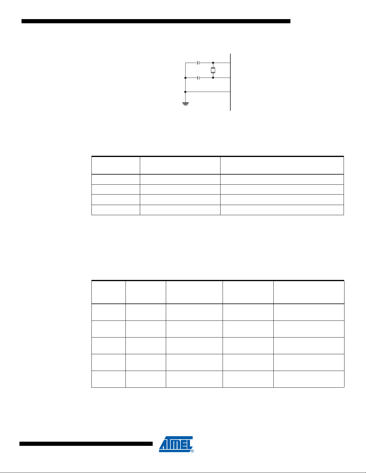
4.2.4 Crystal Oscillator
XTAL1 and XTAL2 are input and output, respectively, of an inverting amplifier which can be configured for use as an On-chip Oscillator, as shown in Figure 4-2. Either a quartz crystal or a
ceramic resonator may be used.
C1 and C2 should always be equal for both crystals and resonators. The optimal value of the
capacitors depends on the crystal or resonator in use, the amount of stray capacitance, and the
electromagnetic noise of the environment. Some initial guidelines for choosing capacitors for
use with crystals are given in Table 4-6. For ceramic resonators, the capacitor values given by
the manufacturer should be used.
SUT1..0
CSUT1..0
(1)
(2)
(3)
00
01 6 CK 14CK + 4.1 ms Fast rising power
10 6 CK 14CK + 65 ms Slowly rising power
11 Reserved
2. CLKSELR register bits
3. This setting is only available if RSTDISBL fuse is not set
Start-up Time from
Power-down/save
6 CK 14CK BOD enabled
Additional Delay
from Reset
(Vcc = 5.0V)
Recommended Usage
26
ATtiny167
7728A–AUTO–07/08
Page 27
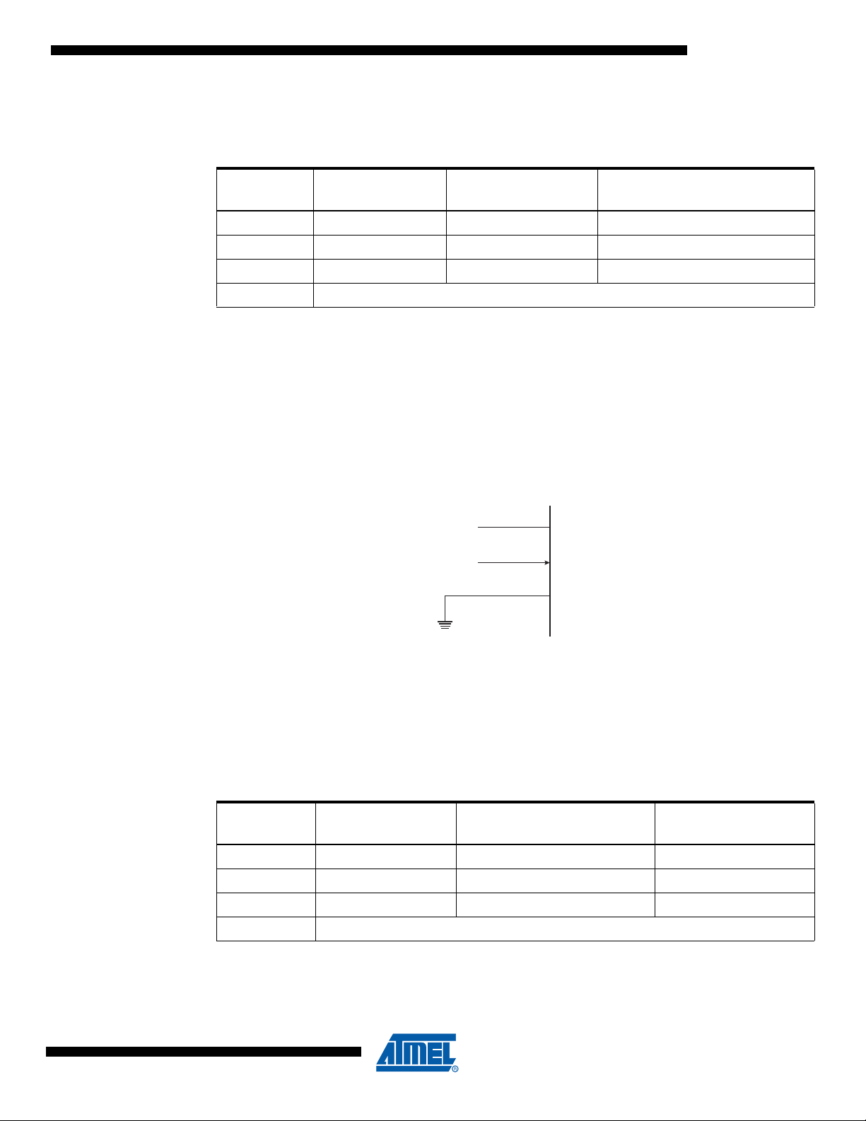
ATtiny167
XTAL2
XTAL1
GND
C2
C1
Figure 4-2. Crystal Oscillator Connections
The Oscillator can operate in three different modes, each optimized for a specific frequency
range. The operating mode is selected by CKSEL3..1 fuses or by CSEL3..1 field as shown in
Table 4-6.
Table 4-6. Crystal Oscillator Operating Modes
CKSEL3..1
CSEL3..1
100
(1)
(2)
(3)
Frequency Range (MHz)
0.4 - 0.9 –
Recommended Range for Capacitors
C1 and C2 for Use with Crystals (pF)
101 0.9 - 3.0 12 - 22
110 3.0 - 8.0 12 - 22
111 8.0 - 16.0 12 - 22
Notes: 1. Flash Fuse bits.
2. CLKSELR register bits.
3. This option should not be used with crystals, only with ceramic resonators.
The CKSEL0 Fuse together with the SUT1..0 Fuses or CSEL0 together with CSUT1..0 field
select the start-up times as shown in Table 4-7.
Table 4-7. Start-up Times for the Crystal Oscillator Clock Selection
CKSEL0
CSEL0
(1)
(2)
SUT1..0
CSUT1..0
(1)
Start-up Time from
(2)
Power-down/save
0 00 258 CK
0 01 258 CK
010
(5)
1K (1024) CK
0 11 1K (1024)CK
1 00 1K (1024)CK
(3)
(3)
(4)
(4)
(4)
Additional Delay
from Reset
(Vcc = 5.0V)
14CK + 4.1 ms
14CK + 65 ms
14CK
14CK + 4.1 ms
14CK + 65 ms
Recommended Usage
Ceramic resonator, fast
rising power
Ceramic resonator, slowly
rising power
Ceramic resonator, BOD
enabled
Ceramic resonator, fast
rising power
Ceramic resonator, slowly
rising power
7728A–AUTO–07/08
27
Page 28
Table 4-7. Start-up Times for the Crystal Oscillator Clock Selection (Continued)
XTAL2
XTAL1
GND
C1=12-22 pF
32.768 KHz
12-22 pF capacitors may be necessary if parasitic
impedance (pads, wires & PCB) is very low.
C2=12-22 pF
(1)
CKSEL0
Notes: 1. Flash Fuse bits.
(2)
CSEL0
101
1 10 16K (16384) CK 14CK + 4.1 ms
1 11 16K (16384) CK 14CK + 65 ms
2. CLKSELR register bits.
3. These options should only be used when not operating close to the maximum frequency of the
4. These options are intended for use with ceramic resonators and will ensure frequency stability
5. This setting is only available if RSTDISBL fuse is not set.
SUT1..0
CSUT1..0
device, and only if frequency stability at start-up is not important for the application. These
options are not suitable for crystals.
at start-up. They can also be used with crystals when not operating close to the maximum frequency of the device, and if frequency stability at start-up is not important for the application.
4.2.5 Low-frequency Crystal Oscillator
To use a 32.768 kHz watch crystal as the clock source for the device, the low-frequency crystal
oscillator must be selected by setting CKSEL fuses or CSEL field as shown in Table 4-1 on page
24. The crystal should be connected as shown in Figure 4-3. Refer to the 32.768 kHz Crystal
Oscillator Application Note for details on oscillator operation and how to choose appropriate values for C1 and C2.
(1)
Start-up Time from
(2)
Power-down/save
(5)
16K (16384) CK 14CK
Additional Delay
from Reset
(Vcc = 5.0V)
Recommended Usage
Crystal Oscillator, BOD
enabled
Crystal Oscillator, fast
rising power
Crystal Oscillator, slowly
rising power
28
The 32.768 kHz watch crystal oscillator can be used by the asynchronous timer if the (high-frequency) Crystal Oscillator is not running or if the External Clock is not enabed (See
”Enable/Disable Clock Source” on page 31.). The asynchronous timer is then able to start itself
this low-frequency crystal oscillator.
Figure 4-3. Low-frequency Crystal Oscillator Connections
ATtiny167
7728A–AUTO–07/08
Page 29
4.2.6 External Clock
(XTAL2)
(CLKO)
CLKI
(XTAL1)
GND
~
External
Clock
Signal
ATtiny167
When this oscillator is selected, start-up times are determined by the SUT fuses or by CSUT
field as shown in Table 4-8.
Table 4-8. Start-up Times for the Low Frequency Crystal Oscillator Clock Selection
SUT1..0
CSUT1..0
Notes: 1. Flash Fuse bits.
To drive the device from this external clock so ur ce, CL KI sho uld be d riven as shown in Figure 4-
4. To run the device on an external clock, the CKSEL Fuses or CSEL field must be programmed
as shown in Table 4-1 on page 24.
(1)
Start-up Time from
(2)
Power-down/save
00 1K (1024) CK
01 1K (1024) CK
10 32K (32768) CK 65 ms Stable frequency at start-up
11 Reserved
2. CLKSELR register bits.
3. These options should only be used if frequency stability at start-up is not important for the
application.
(3)
(3)
Additional Delay from
Reset (Vcc = 5.0V)
4.1 ms Fast rising power or BOD enabled
65 ms Slowly rising power
Recommended usage
Figure 4-4. External Clock Drive Configuration
When this clock source is selected, start-up times are determined by the SUT Fuses or CSUT
field as shown in Table 4-9.
This external clock can be used by the asynchronous timer if the high or low frequency Crystal
Oscillator is not running (See ”Enable/Disable Clock Source” on page 31.). The asynchronous
timer is then able to enable this input.
Table 4-9. Start-up Times for the External Clock Selection
SUT1..0
CSUT1..0
(1)
00 6 CK 14CK (+ 4.1 ms
01 6 CK 14CK + 4.1 ms Fast rising power
10 6 CK 14CK + 65 ms Slowly rising power
Start-up Time from
(2)
Power-down/save
Additional Delay from Reset
(Vcc = 5.0V)
(3)
) BOD enabled
Recommended Usage
7728A–AUTO–07/08
11 Reserved
Notes: 1. Flash Fuse bits.
2. CLKSELR register bits.
3. Additional delay (+ 4ms) available if RSTDISBL fuse is set.
29
Page 30

Note that the System Clock Prescaler can be used to implement run-time changes of the internal
clock frequency while still ensuring stable operation. Refer to ”System Clock Prescaler” on page
36 for details.
4.2.7 Clock Output Buffer
If not using a crystal oscillator, the device can output the system clock on the CLKO pin. To
enable the output, the CKOUT Fuse or COUT bit of CLKSELR register has to be programmed.
This option is useful when the device clock is nee ded to d rive ot her circ uits on th e sys tem. N ote
that the clock will not be output during reset and the normal operation of I/O pin will be overridden when the fuses are programmed. If the System Clock Prescaler is used, it is the divided
system clock that is output.
4.3 Dynamic Clock Switch
4.3.1 Features
The ATtiny167 provides a powerful dynamic clock switch circuit that allows users to turn on and
off clocks of the device on the fly. The built-in de-glitching circuitry allows clocks to be enabled or
disabled asynchronously. This enables efficient power management schemes to be implemented easily and quickly. In a safety application, the dynamic clock switch circuit allows
continuous monitoring of the external clock permitting a fallback scheme in case of clock failure.
The control of the dynamic clock switch circuit must be supervised by software. This operation is
facilitated by the following features:
• Safe commands, to avoid unintentional commands, a special write procedure must be
• Exclusive action, the actions are controlled by a decoding table (commands) written to the
• Command status return. The ‘Request Clock Availability ’ command returns status via the
4.3.2 CLKSELR Register
4.3.2.1 Fuses Substitution
At reset, bits of the Low Fuse Byte are copied into the CL KSELR register. The content of this
register can subsequently be user modified to overwrite the default values from the Low Fuse
Byte. CKSEL3..0, SUT1..0 and CKOUT fuses correspond respectively to CSEL3..0, CSUT1:0
and ~(COUT) bits of the CLKSELR register as shown in Figure 4-5 on page 31.
followed to change the CLKCSR register bits (See Section “4.5.3” on page 38.):
CLKCSR register. This ensures that only one command operation can be launched at any
time. The main actions of the decoding table are:
–‘Disable Clock Source’,
–‘Enable Clock Source’,
–‘Request Clock Availability’,
–‘Clock Source Switching’,
–‘Recover System Clock Source’,
–‘Enable Watchdog in Automatic Reload Mode’.
CLKRDY bit in the CLKCSR register. The ‘Recover System Clock Source ’ command
returns a code of the current clock source in the CLKSELR register. This information is used
in the supervisory software routines as shown in Section 4.3.7 on page 32.
30
ATtiny167
7728A–AUTO–07/08
Page 31

4.3.2.2 Source Selection
CLKSEL[3..0]
SUT[1..0]
CKOUT
Register:
CLKSELR
Fuse:
Fuse Low Byte
CSEL[3..0]
CSUT[1..0]
COUT
Default R/W Reg.
SEL
Decoder
SEL-1
SEL-0
SEL-2
SEL-n
CKSEL[3..0]
SUT[1..0]
SEL
Encoder
EN-1
EN-0
EN-2
EN
-n
CKOUT
Reset
SCLKRq
(*)
SCLKRq
(*)
: Command of Clock Control & Status Register
Internal
Data Bus
Selected
Configuration
Clock
Switch
Current
Configuration
The available codes of clock source are given in Table 4-1 on page 24.
Figure 4-5. Fuses substitution and Clock Source Selection
ATtiny167
4.3.2.3 Source Recovering
4.3.3 Enable/Disable Clock Source
4.3.4 COUT Command
4.3.5 Clock Availability
The CLKSELR register contains the CSEL, CSUT and COUT values which will be used by the
‘Enable/Disable Clock Source’, ‘Request for Clock Availability’ or ‘Clock Source Switching’
commands.
The ‘Recover System Clock Source’ command updates the CKSEL field of CLKSELR register
(See Section “4.3.6” on page 32.).
The ‘Enable Clock Source’ command selects and enables a clock source configured by the settings in the CLKSELR register. CSEL3..0 will select the clock source and CSUT1:0 will select the
start-up time (just as CKSEL and SUT fuse bits do). To be sure that a clock source is operating,
the ‘Request for Clock Availability ’ command must be executed after the ‘Enable Clock Source’
command. This will indicate via the CLKRDY bit in the CLKCSR register that a valid clock source
is available and operational.
The ‘Disable Clock Source’ command disables the clock source indicated by the settings of
CLKSELR register (only CSEL3..0). If the clock source indicated is currently the one that is used
to drive the system clock, the command is not executed.
Because the selected configuration is latched at cloc k source level, it is possib le to en able ma ny
clock sources at a given time (ex: the internal RC oscillator for system clock + an oscillator with
external crystal). The user (code) is responsible of this management.
The ‘CKOUT ’ command allows to drive the CLKO pin. Refer to Section 4.2.7 ”Clock Outp ut
Buffer” on page 30 for using.
‘Request for Clock Availability’ command enables a hardware oscillation cycle counter driven by
the selected source clock, CSEL3..0. The count limit value is determined by the settings of
7728A–AUTO–07/08
31
Page 32

CSUT1..0. The clock is declared ready (CLKRDY = 1) when the count limit value is reached.
The CLKRDY flag is reset when the count starts. Once set, this flag remains unchanged until a
new count is commanded. To perform this checking, the CKSEL and CSUT fields should not be
changed while the operation is running.
Note that once the new clock source is selected (‘Enable Clock Source’ command), the count
procedure is automatically started. The user (code) should wait for the setting of the CLKRDY
flag in CLKSCR register before using a newly selected clock.
At any time, the user (code) can ask for the availability of a clock source. The user (code) can
request it by writing the ‘Request for Clock Availability ’ command in the CLKSCR register. A full
polling of the status of clock sources can thus be done.
4.3.6 System Clock Source Recovering
The ‘Recover System Clock Source’ command returns the current clock source us ed to dr ive the
system clock as per Table 4-1 on page 24. The CKSEL field of CLKSELR register is then
updated with this returned value. There is no information on the SUT used or status on CKOUT.
4.3.7 Clock Switching
To drive the system clock, the user can swit ch from th e curren t clock sour ce to any other of the
following ones (one of them being the current clock source):
1. Calibrated internal RC oscillator 8.0 MHz,
2. Internal watchdog oscillator 128 kHz,
3. External clock,
4. External low-frequency oscillator,
5. External Crystal/Ceramic Resonator. The clock switching is performed by a sequence of commands. First, the user (code) must make sure that the new clock source is operating. Then the ‘Clock Source Switching’ comma nd can be
issued. Once this command has been successfully completed using the ‘Recover System Clock
Source’ command, the user (code) may stop the previous clock source. It is strongly recommended to run this sequence only once the interrupts have been disabled. The user (code) is
responsible for the correct implementation of the clock switching sequence.
32
ATtiny167
7728A–AUTO–07/08
Page 33

Here is a “light” C-code that describes such a sequence of commands.
C Code Example
void ClockSwiching (unsigned char clk_number, unsigned char sut) {
ATtiny167
#define CLOCK
#define CLOCK
#define CLOCK
#define CLOCK_DISABLE 0x01
unsigned char previous
// Disable interrupts
temp = SREG; asm ("cli");
// Save the current system clock source
CLKCSR = 1 << CLKCCE;
CLKCSR = CLOCK
previous_clk = CLKSELR & 0x0F;
// Enable the new clock source
CLKSELR = ((sut << 4 ) & 0x30) | (clk
CLKCSR = 1 << CLKCCE;
CLKCSR = CLOCK_ENABLE;
// Wait for clock validity
while ((CLKCSR & (1 << CLKRDY)) == 0);
// Switch clock source
CLKCSR = 1 << CLKCCE;
CLKCSR = CLOCK
// Wait for effective switching
while (1){
CLKCSR = 1 << CLKCCE;
CLKCSR = CLOCK
if ((CLKSELR & 0x0F) == (clk
}
// Shut down unneeded clock source
if (previous_clk != (clk_number & 0x0F)) {
CLKSELR = previous_clk;
CLKCSR = 1 << CLKCCE;
CLKCSR = CLOCK
}
// Re-enable interrupts
SREG = temp;
}
_RECOVER 0x05
_ENABLE 0x02
_SWITCH 0x04
_clk, temp;
_RECOVER;
_SWITCH;
_RECOVER;
_number & 0x0F)) break;
_DISABLE;
_number & 0x0F);
Warning
4.3.8 Clock Monitoring
A safe system needs to monitor its clock sources. Two domains need to be monitored:
- Clock sources for peripherals,
- Clocks sources for system clock generation.
In the first domain, the user (code) can easily check the validity of the clock(s) (See Section
“4.3.4” on page 31.).
7728A–AUTO–07/08
:
In the ATtiny167, only one among the three external clock sources can be enabled at a
given time. Moreover, the enables of the external clock and of the external low-frequency
oscillator are shared with the asynchronous timer.
33
Page 34

In the second domain, the lack of a clock results in the code not running. Thus, the presence of
Internal Bus
Register:
WDTCSR
WDE
WDP
[3..0]
WDIF
WDIE
Checker
Reload
Enable
System CLK
Automatic
Reloading
Mode
WatchDog Clock
WD
Interrupt
WD
Reset
WatchDog
01
the system clock needs to be monitored by hardware.
Using the on-chip watchdog allows this monitoring. Normally, the watchdog reloading is per-
formed only if the code reaches some specific software labels, reaching these labels p roves that
the system clock is running. Otherwise the watchdog reset is enabled. This behavior can be considered as a clock monitoring.
If the standard watchdog functionality is n ot desired, the ATtiny167 watchdog per mits the system
clock to be monitored without having to resort to the complexity of a full software watchdog handler. The solution proposed in the ATtiny167 is to automate the watchdog reloading with only
one command, at the beginning of the session.
So, to monitor the system clock, the user will have two options:
1. Using the standard watchdog features (software reload),
2. Or using the automatic reloading (hardware reload).
The two options are exclusive.
Note: Warning
:
These two options make sense ONLY if the clock source at RESET is an INTERNAL
SOURCE. The fuse settings determine this operation.
Figure 4-6. Watchdog Timer with Automatic Reloading.
The ‘Enable Watchdog in Automatic Reload Mode’ command has priority over the standard
watchdog enabling. In this mode, only the reset function of the watchdog is enabled (no more
watchdog interrupt). The WDP3..0 bits of the WDTCSR register always determine the watchdog
timer prescaling.
As the watchdog will not be active before executing the ‘Enable Watchdog in Automatic Reload
Mode’ command, it is recommended to activate this command before switching to an external
clock source (See note on page 34).
34
ATtiny167
Note: 1. ONLY the reset (watchdog reset included) disables this function. The Watchdog System Reset
Flag (WDRF bit of MCUSR register) can be used to monitor the reset cause.
2. ONLY clock frequencies
≥ (4 * WatchDog Clock frequency) can be monitored.
7728A–AUTO–07/08
Page 35

ATtiny167
// Enable the watchdog in automatic reload mode
WDTCSR = (1 << WDCE) | (1 << WDE);
WDTCSR = (1 << WDE ) | WD
_2048CYCLES;
CLKCSR = 1 << CLKCCE;
CLKCSR = WD
_ARL_ENABLE;
Here is a “light” C-code of a clock switching function using automatic clock monitoring.
C Code Example
void ClockSwiching (unsigned char clk_number, unsigned char sut) {
#define CLOCK
#define CLOCK
#define CLOCK
#define CLOCK_DISABLE 0x01
#define WD_ARL_ENABLE 0x06
#define WD_2048CYCLES 0x07
unsigned char previous
// Disable interrupts
temp = SREG; asm ("cli");
// Save the current system clock source
CLKCSR = 1 << CLKCCE;
CLKCSR = CLOCK
previous_clk = CLKSELR & 0x0F;
// Enable the new clock source
CLKSELR = ((sut << 4 ) & 0x30) | (clk
CLKCSR = 1 << CLKCCE;
CLKCSR = CLOCK_ENABLE;
// Wait for clock validity
while ((CLKCSR & (1 << CLKRDY)) == 0);
_RECOVER 0x05
_ENABLE 0x02
_SWITCH 0x04
_clk, temp;
_RECOVER;
_number & 0x0F);
// Switch clock source
CLKCSR = 1 << CLKCCE;
CLKCSR = CLOCK
// Wait for effective switching
while (1){
CLKCSR = 1 << CLKCCE;
CLKCSR = CLOCK
if ((CLKSELR & 0x0F) == (clk
}
// Shut down unneeded clock source
if (previous_clk != (clk_number & 0x0F)) {
CLKSELR = previous_clk;
CLKCSR = 1 << CLKCCE;
CLKCSR = CLOCK
}
// Re-enable interrupts
SREG = temp;
}
7728A–AUTO–07/08
_SWITCH;
_RECOVER;
_number & 0x0F)) break;
_DISABLE;
35
Page 36

4.4 System Clock Prescaler
4.4.1 Features
The ATtiny167 system clock can be divided by setting the Clock Prescaler Register – CLKPR.
This feature can be used to decrease power consumption when the requirement for processing
power is low. This can be used with all clock source options, and it will affect the clock frequency
of the CPU and all synchronous peripherals. clk
factor as shown in Table 4-10 on page 38.
4.4.2 Switching Time
When switching between prescaler settings, the System Clock Prescaler ensures that no
glitches occur in the clock system and that no intermediate frequency is higher than neither the
clock frequency corresponding to the previous setting, nor the clock frequency corresponding to
the new setting.
The ripple counter that implements the prescaler runs at the frequency of the undivided clock,
which may be faster than the CPU’s clock frequency. Hence, it is not possible to determine the
state of the prescaler – even if it were readable, and the exact time it takes to switch from one
clock division to another cannot be exactly predicted.
From the time the CLKPS values are written, it takes between T1 + T2 and T1 + 2*T2 before the
new clock frequency is active. In this interval, 2 active clock edges are produced. Here, T1 is the
previous clock period, and T2 is the period corresponding to the new prescaler setting.
I/O
, clk
ADC
, clk
, and clk
CPU
are divided by a
FLASH
4.5 Register Description
4.5.1 OSCCAL – Oscillator Calibration Register
Bit 76543210
CAL7 CAL6 CAL5 CAL4 CAL3 CAL2 CAL1 CAL0 OSCCAL
Read/Write R/W R/W R/W R/W R/W R/W R/W R/W
Initial Value Device Specific Calibration Value
• Bits 7:0 – CAL7:0: Oscillator Calibration Value
The Oscillator Calibration Register is used to trim the Calibrated Internal RC Oscillator to
remove process variations from the oscillator frequency. The factory-calibrated value is automatically written to this register during chip reset, giving an osc illator freq uen cy of 8.0 MHz at 25 °C.
The application software can write this register to change the oscillator frequency. The oscillator
can be calibrated to any frequency in the range 7.3 - 8.1 MHz within ± 2% accuracy. Calibration
outside that range is not guaranteed.
Note that this oscillator is used to time EEPROM and Flash write accesses, and these write
times will be affected accordingly. If the EEPROM or Flash are written, do not calibrate to more
than 8.8 MHz. Otherwise, the EEPROM or Flash write may fail.
The CAL7 bit determines the range of operation for the oscillator. Setting this bit to 0 gives the
lowest frequency range, setting this bit to 1 gives the highest frequency range. The two frequency ranges are overlapping, in other words a setting of OSCCAL = 0x7F gives a higher
frequency than OSCCAL = 0x80.
36
The CAL6..0 bits are used to tune the frequency within the selected range. A setting of 0x00
gives the lowest frequency in that range, and a setting of 0x7F gives the highest frequency in the
ATtiny167
7728A–AUTO–07/08
Page 37

range. Incrementing CAL6..0 by 1 will give a frequency increment of less than 2% in the frequency range 7.3 - 8.1 MHz.
4.5.2 CLKPR – Clock Prescaler Register
Bit 76543210
CLKPCE – – – CLKPS3 CLKPS2 CLKPS1 CLKPS0 CLKPR
Read/Write R/W R R R R/W R/W R/W R/W
Initial Value 0 0 0 0 See Bit Description
• Bit 7 – CLKPCE: Clock Prescaler Change Enable
The CLKPCE bit must be written to logic one to enable change of the CLKPS bits. The CLKPCE
bit is only updated when the other bits in CLKPR are simultaneously written to zero. CLKPCE is
cleared by hardware four cycles after it is written or when the CLKPS bits are written. Rewriting
the CLKPCE bit within this time-out period does neither extend the time-out period, nor clear the
CLKPCE bit.
• Bits 6:4 – Res: Reserved Bits
These bits are reserved bits in the ATtiny167 and will always read as zero.
• Bits 3:0 – CLKPS3:0: Clock Prescaler Select Bits 3 - 0
These bits define the division factor between the selected clock source and the internal system
clock. These bits can be written run-time to vary the clock frequency to suit the application
requirements. As the divider divides the master clock input to the MCU, the speed of all synchronous peripherals is reduced when a division factor is used. The division factors are given in
Table 4-10.
ATtiny167
To avoid unintentional changes of clock frequency, a special write procedure must be followed
to change the CLKPS bits:
1. Write the Clock Prescaler Change Enable (CLKPCE) bit to one and all other bits in
CLKPR to zero.
2. Within four cycles, write the desired value to CLKPS while writing a zero to CLKPCE.
Interrupts must be disabled when changing prescaler setting in order not to disturb th e
procedure.
The CKDIV8 Fuse determines the initial value of the CLKPS bits. If CKDIV8 is unprogrammed,
the CLKPS bits will be reset to “0000”. If CKDIV8 is programmed, CLKPS bits are reset to
“0011”, giving a division factor of eight at start up. This feature should be used if the selecte d
clock source has a higher frequency than the maximum frequency of the device at the present
operating conditions. Note that any value can be written to the CLKPS bits regardless of the
CKDIV8 Fuse setting. The Application software must ensure that a sufficient division factor is
chosen if the selected clock source has a higher frequency than the maximum frequency of the
device at the present operating conditions. The device is shipped with the CKDIV8 Fuse
programmed.
7728A–AUTO–07/08
37
Page 38

Table 4-10. Clock Presc aler Select
CLKPS3 CLKPS2 CLKPS1 CLKPS0 Clock Division Factor
0000 1
0001 2
0010 4
0011 8
0100 16
0101 32
0110 64
0111 128
1000 256
1001 Reserved
1010 Reserved
1011 Reserved
1100 Reserved
1101 Reserved
1110 Reserved
1111 Reserved
4.5.3 CLKCSR – Clock Control & Status Register
Bit 7 6 5 4 3 2 1 0
CLKCCE – – CLKRDY CLKC3 CLKC2 CLKC1 CLKC0 CLKCSR
Read/Write R/W R R R R/W R/W R/W R/W
Initial Value 0 0 0 0 0 0 0 0
• Bit 7 – CLKCCE: Clock Control Change Enable
The CLKCCE bit must be written to logic one to enable change of the CLKCSR bits. The
CLKCCE bit is only updated when the other bits in CLKCSR are simultaneously written to zero.
CLKCCE is cleared by hardware four cycles after it is written or when the CLKCSR bits are written. Rewriting the CLKCCE bit within this time-out period does neither extend the time-out
period, nor clear the CLKCCE bit.
• Bits 6:5 – Res: Reserved Bits
These bits are reserved bits in the ATtiny167 and will always read as zero.
• Bits 4 – CLKRDY: Clock Ready Flag
This flag is the output of the ‘Clock Availability ’ logic.
This flag is cleared by the ‘Request for Clock Availability’ command or ‘Enable Clock Source’
command being entered.
It is set when ‘Clock Availability’ logic confirms that the (selected) clock is running and is stable.
The delay from the request and the flag setting is not fixed, it depends on the clock start-up time,
the clock frequency and, of course, if the clock is alive. The user’s code has to differentiate
between ‘no_clock_signal’ and ‘clock_signal_not_yet_available’ condition.
38
ATtiny167
7728A–AUTO–07/08
Page 39

ATtiny167
• Bits 3:0 – CLKC3:0: Clock Control Bits 3 - 0
These bits define the command to provide to the ‘Clock Switch’ module. The special write procedure must be followed to change the CLKC3..0 bits (See ”Bit 7 – CLKCCE: Clock Control
Change Enable” on page 38.).
1. Write the Clock Control Change Enable (CLKCCE) bit to one and all other bits in
CLKCSR to zero.
2. Within 4 cycles, write the desired value to CLKCSR register while clearing CLKCCE bit.
Interrupts should be disabled when setting CLKCSR register in order not to disturb the
procedure.
Table 4-11. Clock command list.
Clock Command CLKC3..0
No command 0000
Disable clock source 0001
Enable clock source 0010
Request for clock availability 0011
Clock source switch 0100
Recover system clock source code 0101
Enable watchdog in automatic reload mode 0110
CKOUT command 0111
No command 1
xxx
b
b
b
b
b
b
b
b
b
4.5.4 CLKSELR - Clock Selection Register
Bit 7 6 543210
- COUT CSUT1 CSUT0 CSEL3 CSEL2 CSEL1 CSEL0 CLKSELR
Read/Write R R/W R/W R/W R/W R/W R/W R/W
Initial Value 0 ~ (CKOUT)
• Bit 7– Res: Reserved Bit
This bit is reserved bit in the ATtiny167 and will always read as zero.
• Bit 6 – COUT: Clock Out
The COUT bit is initialized with ~(CKOUT) Fuse bit.
The COUT bit is only used in case of ‘CKOUT’ command. Refer to Section 4.2.7 ”Clock Output
Buffer” on page 30 for using.
In case of ‘Recover System Clock Source’ command, COUT it is not affected (no recovering of
this setting).
• Bits 5:4 – CSUT1:0: Clock Start-up Time
CSUT bits are initialized with the values of SUT Fuse bits.
In case of ‘Enable/Disable Clock Source’ command, CSUT field provides the code of the clock
start-up time. Refer to subdivisions of Section 4.2 ”Clock Sources” on page 24 for code of clock
start-up times.
fuse
SUT1..0
fuses
CKSEL3..0
fuses
7728A–AUTO–07/08
39
Page 40

In case of ‘Recover System Clock Source’ command, CSUT field is not affected (no recovering
of SUT code).
• Bits 3:0 – CSEL3:0: Clock Source Select
CSEL bits are initialized with the values of CKSEL Fuse bits.
In case of ‘Enable/Disable Clock Source’, ‘Request for Clock Availability’ or ‘Clock Source
Switch’ command, CSEL field provides the code of the clock source. Refer to Ta ble 4-1 on page
24 and subdivisions of Section 4.2 ”Clock Sources” on page 24 for clock source codes.
In case of ‘Recover System Clock Source’ command, CSEL field contains the code of the clock
source used to drive the Clock Control Unit as described in Figure 4-1 on page 23.
40
ATtiny167
7728A–AUTO–07/08
Page 41

5. Power Management and Sleep Modes
Sleep modes enable the application to shut down unused modules in the MCU, thereby saving
power. The AVR provides various sleep modes allowing the user to tailor the po wer consumption to the application’s requirements.
When enabled, the Brown-out Detector (BOD) actively monitors the power supply voltage during
the sleep periods. To further save power, it is possible to d isable th e BOD in some sleep modes.
See ”BOD Disable” on page 41 for more details.
5.1 Sleep Modes
Figure 4-1 on page 23 presents the different clock systems in the ATtiny167, and their distribu-
tion. The figure is helpful in selecting an appropriate sleep mode. Table 5-1 shows the different
sleep modes, their wake up sources and BOD disable ability.
Table 5-1. Active Clock Domains and Wake-up Sources in the Different Sleep Modes
Active Clock Domains Oscillators Wake-up Sources
ATtiny167
5.2 BOD Disable
CPU
FLASH
clk
Sleep Mode
Idle XXX X X X XXXXXX
ADC Noise
Reduction
Power-down X
Power-Save X X X
Note: 1. For INT1 and INT0, only level interrupt.
clk
ADC
ASY
clkIOclk
clk
Main Clock
Source Enabled
Timer0 Osc.
XX X X X
Software
Enable
INT1, INT0 and
Pin Change
SPM/EEPROM
Ready
ADC
WDT
USI Start Condition
Timer0
(1)
X XXXX
(1)
(1)
XX X
XXX X
Other I/O
BOD Disable
To enter any of the four sleep modes, the SE bit in SMCR must be written to logic one and a
SLEEP instruction must be executed. The SM1, and SM0 bits in the SMCR Register select
which sleep mode (Idle, ADC Noise Reduction, Power-down, or Power-save) will be activated by
the SLEEP instruction. See Table 5-2 on page 45 for a summary.
If an enabled interrupt occurs while the MCU is in a sleep mode, the MCU wakes up. The MCU
is then halted for four cycles in addition to the start-up time, executes the interrupt routine, and
resumes execution from the instruction following SLEEP. The contents of the Register File and
SRAM are unaltered when the device wakes up from sleep. If a r eset occurs duri ng sle ep mod e,
the MCU wakes up and executes from the Reset Vector.
When the Brown-out Detector (BOD) is enabled by BODLEVEL fuses, Table 21-3 on page 217,
the BOD is actively monitoring the power supply voltage during a sleep period. To save power, it
is possible to disable the BOD by software for some of the sleep modes, see Table 5-1. The
sleep mode power consumption will then be at the same level as when BOD is globally disabled
by fuses. If BOD is disabled in software, the BOD function is turned off immediately after enter-
7728A–AUTO–07/08
41
Page 42

5.3 Idle Mode
ing the sleep mode. Upon wake-up from sleep, BOD is automatically enabled again. This
ensures safe operation in case the Vcc level has dropped during the sleep period.
When the BOD has been disabled, the wake-up time from sleep mode will be approximately 60
µs to ensure that the BOD is working correctly before the MCU continues executing code.
BOD disable is controlled by BODS bit (BOD Sleep) in the control register MCUCR, see
”MCUCR – MCU Control Register” on page 45. Setting it to one turns off the BOD in relevant
sleep modes, while a zero in this bit keeps BOD active. Default setting keeps BOD active, i.e.
BODS is cleared to zero.
Writing to the BODS bit is controlled by a timed sequence and an enable bit, see ”MCUCR –
MCU Control Register” on page 45.
When the SM1..0 bits are written to 00, the SLEEP instruction makes the MCU enter Idle mode,
stopping the CPU but allowing the SPI, Analog Comparator, ADC, USI start condition, Asynchronous Timer/Counter, Watchdog, and the interrupt system to continue operating. This sleep
mode basically halts clk
CPU
and clk
, while allowing the other clocks to run.
FLASH
Idle mode enables the MCU to wake up from external triggered interrupts as well as internal
ones like the SPI interrupts. If wake-up from the Analog Comparator interrupt is not required, the
Analog Comparator can be powered down by setting the ACD bit in the Analog Comparator
Control and Status Register – ACSR. This will reduce power consumption in Idle mode. If th e
ADC is enabled, a conversion starts automatically when this mode is entered.
5.4 ADC Noise Reduction Mode
When the SM1..0 bits are written to 01, the SLEEP instruction makes the MCU enter ADC Noise
Reduction mode, stopping the CPU but allowing the ADC, the external interrupts, the USI start
condition, the asynchronous Timer/Counter and the Watchdog to con tinue operating (if
enabled). This sleep mode basically halts clk
clocks to run.
This improves the noise environment for the ADC, enabling higher resolution measurements. If
the ADC is enabled, a conversion starts automatically when this mode is entered. Apart from the
ADC Conversion Complete interrupt, only an External Reset, a Watchdog System Reset, a
Watchdog Interrupt, a Brown-out Reset, a USI start condition inter rupt, an asynchronous
Timer/Counter interrupt, an SPM/EEPROM ready interrupt, an external level interrupt on INT0 or
INT1 or a pin change interrupt can wake up the MCU from ADC Noise Reduction mode.
5.5 Power-down Mode
When the SM1..0 bits are written to 10, the SLEEP instruction makes the MCU enter Powerdown mode. In this mode, the external Oscillator is stopped, while the external interrupts, the
USI start condition, and the Watchdog continue operating (if enabled). Only an External Reset, a
Watchdog System Reset, a Watchdog Interrupt, a Brown-out Reset, the USI start condition
interrupt, an external level interrupt on INT0 or INT1, or a pin change interrupt can wake up the
MCU. This sleep mode basically halts all generated clocks, allowing operation of asynchronous
modules only.
I/O
, clk
, and clk
CPU
, while allowing the other
FLASH
42
Note that if a level triggered interrupt is used for wake-up from Power-down mode, the changed
level must be held for some time to wake up the MCU. Refer to Section 8. ”External Interrupts”
on page 59 for details.
ATtiny167
7728A–AUTO–07/08
Page 43

When waking up from Power-down mode, there is a delay from the wake-up condition occurs
until the wake-up becomes effective. This allows the clock to restart and become stable after
having been stopped. The wake-up period is defined by the same CKSEL Fuses that define the
Reset Time-out period, as described in Section 4.2 ”Clock Sources” on page 24.
5.6 Power-save Mode
When the SM1..0 bits are written to 11, the SLEEP instruction makes the MCU enter Powersave mode. This mode is identical to Power-down, with one exception:
If Timer/Counter0 is clocked asynchronously, i.e., the AS0 bit in ASSR is set, Timer/Counter0
will run during sleep. The device can wake up from either Timer Overflow or Output Compare
event from Timer/Counter0 if the corresponding Timer/Counter0 interrupt enable bits are set in
TIMSK0, and the global interrupt enable bit in SREG is set.
If the Asynchronous Timer is NOT clocked asynchronously, Power-down mode is recommended
instead of Power-save mode because the contents of the re gisters in the asynchronous tim er
should be considered undefined after wake-up in Power-save mode if AS0 is 0.
ATtiny167
This sleep mode basically halts all clocks except clk
modules, including Timer/Counter0 if clocke d as yn ch ro nously.
5.7 Power Reduction Register
The Power Reduction Register (PRR), see ”PRR – Power Reduction Register” on page 46, pro-
vides a method to stop the clock to individual peripherals to reduce power consumption. The
current state of the peripheral is frozen and the I/O registers can not be read or written.
Resources used by the peripheral when stopping the clock will remain occupied, hence the
peripheral should in most cases be disabled before stopping the clock. Waking up a module,
which is done by clearing the bit in PRR, puts the module in the same state as before shutdo wn.
Module shutdown can be used in Idle mode and Active mode to significantly reduce the overall
power consumption. In all other sleep modes, the clock is already stopped.
5.8 Minimizing Power Consumption
There are several possibilities to consider when trying to minimize the power consumption in an
AVR controlled system. In general, sleep modes should be used as much as possible, and the
sleep mode should be selected so that as few as possible of the device’s functions are operating. All functions not needed should be disabled. In particular, the following modules may need
special consideration when trying to achieve the lowest possible power consumption.
5.8.1 Analog to Digital Converter
If enabled, the ADC will be enabled in all sleep modes. To save power, the ADC should be disabled before entering any sleep mode. When the ADC is turned off and on again, the next
conversion will be an extended conversion. Refer to Section 17. ”ADC – Analog to Digital Con-
verter” on page 183 for details on ADC operation.
, allowing operation only of asynchronous
ASY
5.8.2 Analog Comparator
When entering Idle mode, the Analog Comparator should be disabled if not used. When entering
ADC Noise Reduction mode, the Analog Comparator should be disabled. In other sleep modes,
the Analog Comparator is automatically disabled. However, if the Analog Comparator is set up
to use the Internal Voltage Reference as input, the Analog Comparat or shou ld be d isable d in all
sleep modes. Otherwise, the Internal Voltage Reference will be enabled, independe nt of sleep
7728A–AUTO–07/08
43
Page 44

mode. Refer to Section 18. ”AnaComp - Analog Comparator” on page 202 for details on how to
configure the Analog Comparator.
5.8.3 Brown-out Detector
If the Brown-out Detector is not needed by the a pplication, this modu le should be turned off . If
the Brown-out Detector is enabled by the BODLEVEL Fuses, it will be enabled in all sleep
modes, and hence, always consume power. In the deeper sleep modes, this will contribute significantly to the total current consumption. Refe r to Sec tio n 6. 1.5 ”Brown-out Detection” on page
49 for details on how to configure the Brown-out Detector.
5.8.4 Internal Voltage Reference
The Internal Voltage Reference will be enabled when needed by the Brown-out Detection, the
Analog Comparator or the ADC. If these modules are disabled as described in the sections
above, the internal voltage reference will be disabled and it will not be consuming power. When
turned on again, the user must allow the reference to start up before the output is used. If the
reference is kept on in sleep mode, the output can be used immediately. Refer to Section 6.2
”Internal Voltage Reference” on page 51 for details on the start-up time.
Output the internal voltage reference is not needed in the deeper sleep modes. This module
should be turned off to reduce significantly to the total current consumption. Refer to ”AMISCR –
Analog Miscellaneous Control Register” on page 201 for details on how to disable the internal
voltage reference output.
5.8.5 Internal Current Source
The Internal Current Source is not needed in the deeper sleep modes. This module should be
turned off to reduce significantly to the total current consumption. Refer to ”AMISCR – Analog
Miscellaneous Control Register” on page 182 for deta ils on how to disable the Internal Current
Source.
5.8.6 Watchdog T imer
If the Watchdog Timer is not needed in the application, the module should be turned off. If the
Watchdog Timer is enabled, it will be enabled in all sleep modes and hence always consume
power. In the deeper sleep modes, this will contribute significantly to the total current consumption. Refer to Section 6.3 ”Watchdog Timer” on page 51 for details on how to configure the
Watchdog Timer.
5.8.7 Port Pins
When entering a sleep mode, all port pins should be configured to use minimum power. The
most important is then to ensure that no pins drive resistive loads. In sleep modes where both
the I/O clock (clk
be disabled. This ensures that no power is consumed by the input logic when not needed. In
some cases, the input logic is needed for detecting wake-up conditions, and it will then be
enabled. Refer to the section Section 9.2.6 ”Digital Input Enable and Sleep Modes” on page 69
for details on which pins are enabled. If the input buffer is enabled and the input signal is left
floating or have an analog signal level close to Vcc/2, the input buffer will use excessive power.
) and the ADC clock (clk
I/O
) are stopped, the input buffers of the device will
ADC
44
For analog input pins, the digital input buffer should be disabled at all times. An analog signal
level close to Vcc/2 on an input pin can cause significant current even in active mode. Digital
input buffers can be disabled by writing to the Digital Input Disable Registers (DIDR1 and
DIDR0). Refer to Section 17.11.6 ”DIDR1 – Digital Input Disable Register 1” on page 201 and
Section 17.11.5 ”DIDR0 – Digital Input Disable Register 0” on page 200 for details.
ATtiny167
7728A–AUTO–07/08
Page 45

5.8.8 On-chip Debug System
If the On-chip debug system is enabled by the DWEN Fuse and the chip enters sleep mode, the
main clock source is enabled and hence always consumes power. In the deeper sleep modes,
this will contribute significantly to the total current consumption.
5.9 Register Description
5.9.1 SMCR – Sleep Mode Control Register
The Sleep Mode Control Register contains control bits for power management.
Bit 76543210
– – – – – SM1 SM0 SE SMCR
Read/Write RRRRRR/WR/WR/W
Initial Value 0 0 0 0 0 0 0 0
• Bits 7..3 Res: Reserved Bits
These bits are unused bits in the ATtiny167, and will always read as zero.
• Bits 2..1 – SM1..0: Sleep Mode Select Bits 1, and 0
These bits select between the four available sleep modes as shown in Table 5-2.
ATtiny167
Table 5-2. Sleep Mode Select
SM1 SM0 Sleep Mode
00Idle
0 1 ADC Noise Reduction
1 0 Power-down
1 1 Power-save
• Bit 0 – SE: Sleep Enable
The SE bit must be written to logic one to make the MCU enter the sleep mode when the SLEEP
instruction is executed. To avoid the MCU entering the sleep mode unless it is the programmer’s
purpose, it is recommended to write the Sleep Enab le (SE) bit to one just before the exec ution of
the SLEEP instruction and to clear it immediately after waking up.
5.9.2 MCUCR – MCU Control Register
Bit 7 6 5 4 3 2 1 0
– BODS BODSE PUD – – – – MCUCR
Read/Write R R/W R/W R/W R R R R
Initial Value 0 0 0 0 0 0 0 0
• Bit 6 – BODS: BOD Sleep
The BODS bit must be written to logic one in order to turn off BOD during sleep, see Table 5-1
on page 41. Writing to the BODS bit is controlled by a timed sequence and an enable bit,
BODSE in MCUCR. To disable BOD in relevant sleep modes, both BODS and BODSE must first
be set to one. Then, to set the BODS bit, BODS must be set to one and BODSE must be set to
zero within four clock cycles.
7728A–AUTO–07/08
45
Page 46

The BODS bit is active three clock cycles after it is set. A sleep instruction must be executed
while BODS is active in order to turn off the BOD for the actual sleep mode. The BODS bit is
automatically cleared after three clock cycles.
• Bit 5 – BODSE: BOD Sleep Enable
BODSE enables setting of BODS control bit, as explained in BODS bit description. BOD disable
is controlled by a timed sequence.
5.9.3 PRR – Power Reduction Register
Bit 76543210
– – PRLIN PRSPI PRTIM1 PRTIM0 PRUSI PRADC PRR
Read/Write R/W R R/W R/W R/W R/W R/W R/W
Initial Value00000000
• Bit 7 - Res: Reserved bit
This bit is reserved in ATtiny167 and will always read as zero.
• Bit 6 - Res: Reserved bit
This bit is reserved in ATtiny167 and will always read as zero.
• Bit5 - PRLIN: Power Reduction LIN / UART controller
Writing a logic one to this bit shuts down the LIN by stopping the clock to the module. When
waking up the LIN again, the LIN should be re initialized to ensure proper operation.
• Bit 4 - PRSPI: Power Reduction Serial Peripheral Interface
If using debugWIRE On-chip Debug System, this bit should not be written to one.
Writing a logic one to this bit shuts down the Serial Peripheral Interface by stopping the clock to
the module. When waking up the SPI again, the SPI should be re initialized to ensure proper
operation.
• Bit 3 - PRTIM1: Power Reduction Timer/Counter1
Writing a logic one to this bit shuts down the Timer/Counter1 module. When the Timer/Counter1
is enabled, operation will continue like before the shutdown.
• Bit 2 - PRTIM0: Power Reduction Timer/Counter0
Writing a logic one to this bit shuts down the Timer/Co unte r0 module in synchrono us mode ( AS0
is 0). When the Timer/Counter0 is enabled, operation will continue like before the shutdown.
• Bit 1 - PRUSI: Power Reduction USI
Writing a logic one to this bit shuts down the USI by stopping the clock to the module. When
waking up the USI again, the USI should be re-initialized to ensure proper operation.
• Bit 0 - PRADC: Power Reduction ADC
Writing a logic one to this bit shuts down the ADC. The ADC must be disa bled before sh ut down.
The analog comparator cannot use the ADC input MUX when the ADC is shut down.
46
ATtiny167
7728A–AUTO–07/08
Page 47

6. System Control and Reset
6.1 Reset
6.1.1 Resetting the AVR
During reset, all I/O Registers are set to their initial values, and the program starts execution
from the Reset Vector. The instruction placed at the Reset Vector must be an RJMP – Relative
Jump – instruction to the reset handling routine. If the program never enables an interrupt
source, the Interrupt Vectors are not used, and regular program code can be placed at these
locations. The circuit diagram in Figure 6-1 shows the reset circuit. Tables in Section 22.5
”RESET Characteristics” on page 236 defines the electrical parameters of the reset circuitry.
The I/O ports of the AVR are immediately reset to their initial state when a reset source goes
active. This does not require any clock source to be running.
After all reset sources have gone inactive, a delay counter is invoked, stretching the internal
reset. This allows the power to reach a stable level before normal operation starts. The time-out
period of the delay counter is defined by the user through the SUT and CKSEL Fuses. The different selections for the delay period are presented in Section 4.2 ”Clock Sources” on page 24 .
6.1.2 Reset Sources
The ATtiny167 has four sources of reset:
ATtiny167
• Power-on Reset. The MCU is reset when the supply voltage is below the Power-on Reset
threshold (V
• External Reset. The MCU is reset when a low level is present on the RESET
than the minimum pulse length.
• Watchdog System Reset. The MCU is reset when the Watchdog Timer period expires and
the Watchdog System Reset mode is enabled.
• Brown-out Reset. The MCU is reset when the supply voltage Vcc is below the Brown-out
Reset threshold (V
POT
).
) and the Brown-out Detector is enabled.
BOT
pin for longer
7728A–AUTO–07/08
47
Page 48

Figure 6-1. Reset Circuit
MCU Status
Register (MCUSR)
Brown-out
Reset Circuit
BODLEVEL [2..0]
Delay Counters
CKSEL[3:0]
CK
TIMEOUT
WDRF
BORF
EXTRF
PORF
DATA BUS
Clock
Generator
Spike
Filter
Pull-up Resistor
Watchdog
Oscillator
SUT[1:0]
Power-on Reset
Circuit
RSTDISBL
V
TIME-OUT
INTERNAL
RESET
t
TOUT
V
POT
V
PORMAX
V
PORMIN
CC
V
CCRR
6.1.3 Power-on Reset
48
ATtiny167
A Power-on Reset (POR) pulse is generated by an On-chip detection circuit. The detection level
is defined in Table 22-4 on page 236. The POR is activated whenever Vcc is below the detection
level. The POR circuit can be used to trigger the start-up Reset, as well as to detect a failure in
supply voltage.
A Power-on Reset (POR) circuit ensures that the device is reset from Power-on. Reac hing the
Power-on Reset threshold voltage invokes the delay counter, which determines how long the
device is kept in RESET after Vcc rise. The RESET signal is activated again, without any delay,
when Vcc decreases below the detection level.
Figure 6-2. MCU Start-up, RESET
Tied to Vcc
7728A–AUTO–07/08
Page 49

6.1.4 External Reset
V
RESET
TIME-OUT
INTERNAL
RESET
t
TOUT
V
RST
V
POR
CC
V
CCRR
CC
ATtiny167
Figure 6-3. MCU Start-up, RESET Extended Externally
An External Reset is generated by a low level on the RESET
minimum pulse width (see Table 22-3 on page 236) will generate a reset, even if the clock is not
running. Shorter pulses are not guaranteed to gene rate a reset. When the applied signal
reaches the Reset Threshold Voltage – V
MCU after the Time-out period – t
TOUT –
– on its positive edge, the delay counter starts the
RST
has expired. The External Reset can be disabled by the
RSTDISBL fuse, see Table 21-4 on page 217.
pin. Reset pulses longer than the
6.1.5 Brown-out Detection
Figure 6-4. External Reset During Operation
ATtiny167 has an On-chip Brown-out Detection (BOD) circuit for monitoring the Vcc level during
operation by comparing it to a fixed trigger level. The trigger level for the BOD can be selected
by the BODLEVEL Fuses (See ”BODLEVEL Fuse Coding” on page 237.). The trigger level has
a hysteresis to ensure spike free Brown-out Detection. The hysteresis on the detection level
should be interpreted as V
When the BOD is enabled, and Vcc decreases to a value below the trigger level (V
BOT
= V
+
BOT
+ V
HYST
/ 2 and V
BOT
= V
–
BOT
- V
HYST
/ 2.
BOT
–
in Figure
6-5), the Brown-out Reset is immediately activated. When Vcc increases above the trigger level
(V
in Figure 6-5), the delay counter starts the MCU after the Time-out period t
BOT
+
TOUT
has
expired.
The BOD circuit will only detect a drop in Vcc if the voltage stays below the trigger level for
longer than t
given in Table 22-6 on page 237.
BOD
7728A–AUTO–07/08
49
Page 50

Figure 6-5. Brown-out Reset During Operation
V
CC
RESET
TIME-OUT
INTERNAL
RESET
V
BOT-
V
BOT+
t
TOUT
CK
CC
6.1.6 Watchdog System Reset
When the Watchdog times out, it will generate a short reset pulse of one CK cycle duration. On
the falling edge of this pulse, the delay timer starts counting the Time-out period t
page 51 for details on operation of the Watchdog Timer.
Figure 6-6. Watchdog System Reset During Operation
TOUT
. Refer to
6.1.7 MCU Status Register – MCUSR
The MCU Status Register provides information on which reset source caused an MCU reset.
Bit 76543210
Read/Write RRRRR/WR/WR/WR/W
Initial Value0000 See Bit Description
• Bit 7..4 – Res: Reserved Bits
These bits are unused bits in the ATtiny167, and will always read as zero.
• Bit 3 – WDRF: Watchdog System Reset Flag
This bit is set if a Watchdog System Reset occurs. The bit is reset by a Power-on Reset, or by
writing a logic zero to the flag.
• Bit 2 – BORF: Brown-out Reset Flag
This bit is set if a Brown-out Reset occurs. The bit is reset by a Power-on Reset, or by writing a
logic zero to the flag.
50
ATtiny167
––––WDRFBORFEXTRFPORFMCUSR
7728A–AUTO–07/08
Page 51

• Bit 1 – EXTRF: External Reset Flag
This bit is set if an External Reset occurs. The bit is reset by a Power-on Reset, or by writing a
logic zero to the flag.
• Bit 0 – PORF: Power-on Reset Flag
This bit is set if a Power-on Reset occurs. The bit is reset only by writing a logic zero to the flag.
To make use of the Reset Flags to identify a reset condition, the user should read and then
Reset the MCUSR as early as possible in the program. If the register is cleared before another
reset occurs, the source of the reset can be found by examining the Reset Flags.
6.2 Internal Voltage Reference
ATtiny167 features an internal bandgap reference. This reference is used for Brown-out Detection, and it can be used as an input to the Analog Comparator or the ADC.
6.2.1 Voltage Reference Enable Signals and Start-up Time
The voltage reference has a start-up time that may influence the way it should be used. The
start-up time is given in Table 22-7 on page 237. To save power, the reference is not always
turned on. The reference is on during the following situations:
1. When the BOD is enabled (by programming the BODLEVEL [2:0] Fuses).
2. When the bandgap reference is connected to the Analog Comparator (by setting the
ACIRS bit in ACSR).
3. When the ADC is enabled.
Thus, when the BOD is not enabled, after setting the ACIRS bit or enabling the ADC, the user
must always allow the reference to start up before the output from the Analog Comparator or
ADC is used. To reduce power consumption in Power-down mode or in Power-save, the user
can avoid the three conditions above to ensure that the reference is turned off before entering in
these power reduction modes.
ATtiny167
6.3 Watchdog Timer
ATtiny167 has an Enhanced Watchdog Timer (WDT). The main features are:
•
Clocked from separate On-chip Oscillator
• 4 Operating modes
–Interrupt
– System Reset
– Interrupt and System Reset
– Clock Monitoring
• Selectable Time-out period from 16ms to 8s
• Possible Hardware fuse Watchdog always on (WDTON) for fail-safe mode
6.3.1 Watchdog Timer Behavior
The Watchdog Timer (WDT) is a timer counting cycles of a separate on-chip 128 KHz oscillator.
7728A–AUTO–07/08
51
Page 52

Figure 6-7. Watchdog Timer
MCU
RESET
WATCHDOG
RESET
CLOCK
MONITORING
INTERRUPT
WDE
WDIF
WDIE
WDP0
WDP1
WDP2
WDP3
OSC / 1024K
OSC / 512K
OSC / 4K
OSC / 2K
OSC / 256K
OSC / 128K
OSC / 64K
OSC / 32K
OSC / 16K
OSC / 8K
WATCHDOG
PRESCALER
~128 KHz
OSCILLATOR
The WDT gives an interrupt or a system reset when the counter reaches a given time-out value.
In normal operation mode, it is required that the system uses the WDR - Watchdog Timer Reset
- instruction to restart the counter before the time-out value is reached. If the system doesn't
restart the counter, an interrupt or system reset will be issued.
In Interrupt mode, the WDT gives an interrupt when the timer expires. T his inter rupt can be used
to wake the device from sleep-modes, and also as a general system timer. One example is to
limit the maximum time allowed for certain operations, giving an interrupt when the operation
has run longer than expected. In System Reset mode, the WDT gives a reset when the timer
expires. This is typically used to prevent system hang-up in case of runaway code. The third
mode, Interrupt and System Reset mode, combines the other two modes by first giving an interrupt and then switch to System Reset mode. This mode will for instance allow a safe shutdown
by saving critical parameters before a system reset.
52
The Watchdog always on (WDTON) fuse, if programmed, will force the Watchdog Timer to
System Reset mode. With the fuse programmed the System Reset mode bit (WDE) and Interrupt mode bit (WDIE) are locked to 1 and 0 respectively. To further ensure program security,
alterations to the Watchdog set-up must follow timed sequences. The sequence for clearing
WDE and changing time-out configuration is as follows:
1. In the same operation, write a logic one to the Watchdog change enable b it ( WDCE) and
2. Within the next four clock cycles, write the WDE and Watchdog prescaler bits (WDP) as
ATtiny167
WDE. A logic one must be written to WDE regardless of the previous value of the WDE
bit.
desired, but with the WDCE bit cleared. This must be done in one operation.
7728A–AUTO–07/08
Page 53

ATtiny167
The following code example shows one assembly and one C function for turning off the Watchdog Timer. The example assumes that interrupts are controlled (e.g. by disabling interrupts
globally) so that no interrupts will occur during the execution of these functions.
Assembly Code Example
WDT_off:
; Turn off global interrupt
cli
; Reset Watchdog Timer
wdr
; Clear WDRF in MCUSR
in r16, MCUSR
andi r16, (0xff & (0<<WDRF))
out MCUSR, r16
; Write logical one to WDCE and WDE
; Keep old prescaler setting to prevent unintentional time-out
lds r16, WDTCR
ori r16, (1<<WDCE) | (1<<WDE)
sts WDTCR, r16
; Turn off WDT
ldi r16, (0<<WDE)
sts WDTCR, r16
; Turn on global interrupt
sei
ret
C Code Example
(1)
(1)
void WDT_off(void)
{
__disable_interrupt();
__watchdog_reset();
/* Clear WDRF in MCUSR */
MCUSR &= ~(1<<WDRF);
/* Write logical one to WDCE and WDE */
/* Keep old prescaler setting to prevent unintentional time-out */
WDTCR |= (1<<WDCE) | (1<<WDE);
/* Turn off WDT */
WDTCR = 0x00;
__enable_interrupt();
}
Note: 1. See ”About Code Examples” on page 5.
Note: If the Watchdog is accidentally enabled, for example by a runaway pointer or brown-out
condition, the device will be reset and the Watchdog Timer will stay enabled. If the code is n ot
set up to handle the Watchdog, this might lead to an eternal loop of time-out resets. To avoid this
situation, the application software should always clear the Watchdog System Reset Flag
(WDRF) and the WDE control bit in the initialization routine, even if the Watchdog is not in use.
7728A–AUTO–07/08
53
Page 54

The following code example shows one assembly and one C function for changing the time-out
value of the Watchdog Timer.
Assembly Code Example
WDT_Prescaler_Change:
; Turn off global interrupt
cli
; Reset Watchdog Timer
wdr
; Start timed sequence
lds r16, WDTCR
ori r16, (1<<WDCE) | (1<<WDE)
sts WDTCR, r16
; -- Got four cycles to set the new values from here -
; Set new prescaler(time-out) value = 64K cycles (~0.5 s)
ldi r16, (1<<WDE) | (1<<WDP2) | (1<<WDP0)
sts WDTCR, r16
; -- Finished setting new values, used 2 cycles -
; Turn on global interrupt
sei
ret
C Code Example
(1)
(1)
Note: 1. See ”About Code Examples” on page 5.
6.3.2 Clock monitoring
The Watchdog Timer can be used to detect a loss of system clock. This configuration is driven
by the dynamic clock switch circuit. Please refer to Section 4.3.8 ”Clock Monitoring” on page 33
for more information.
void WDT_Prescaler_Change(void)
{
__disable_interrupt();
__watchdog_reset();
/* Start timed sequence */
WDTCR |= (1<<WDCE) | (1<<WDE);
/* Set new prescaler(time-out) value = 64K cycles (~0.5 s) */
WDTCR = (1<<WDE) | (1<<WDP2) | (1<<WDP0);
__enable_interrupt();
}
2. The Watchdog Timer should be reset before any change of the WDP bits, since a change in
the WDP bits can result in a time-out when switching to a shorter time-out period.
54
ATtiny167
7728A–AUTO–07/08
Page 55

6.3.3 Watchdog Ti mer Control Register - WDTCR
Bit 76543210
WDIF WDIE WDP3 WDCE WDE WDP2 WDP1 WDP0 WDTCR
Read/Write R/W R/W R/W R/W R/W R/W R/W R/W
Initial Value 0 0 0 0 X 0 0 0
• Bit 7 - WDIF: Watchdog Interrupt Flag
This bit is set when a time-out occurs in the Watchdog Timer and the Watchdog Timer is configured for interrupt. WDIF is cleared by hardware when executing the corresponding interrupt
handling vector. Alternatively, WDIF is cleared by writing a logic on e to the flag. When the I-bit in
SREG and WDIE are set, the Watchdog Time-out Interrupt is executed.
• Bit 6 - WDIE: Watchdog Interrupt Enable
When this bit is written to one and the I-bit in the Status Register is set, the Watchdog Interrupt is
enabled. If WDE is cleared in combination with this setting, the Watchdog Timer is in Interrupt
Mode, and the corresponding interrupt is executed if time-out in the Watchdog Timer occurs.
If WDE is set, the Watchdog Timer is in Interrupt and System Reset Mode. The first time-out in
the Watchdog Timer will set WDIF. Executing the corresponding interrupt vector will clear WDIE
and WDIF automatically by hardware (the Watchdog goes to System Reset Mode). This is
useful for keeping the Watchdog Timer security while u sing the in terrup t. To stay in Inte rrupt and
System Reset Mode, WDIE must be set after each interrupt. This sho uld however not be don e
within the interrupt service routine itself, as this might compromise the safety-function of the
Watchdog System Reset mode. If the interrupt is not executed before the next time-out, a
System Reset will be applied.
ATtiny167
If the Watchdog Timer is used as clock monitor (c.f. Section • ”Bits 3:0 – CLKC3:0: Clock Control
Bits 3 - 0” on page 39), the System Reset Mode is enabled and the Interrupt Mode is automati-
cally disabled.
Table 6-1. Watchdog Timer Configuration
Clock
Monitor
x 0 0 0 Stopped None
On y
Off
Note: 1. At least one of these three enables (WDTON, WDE & WDIE) equal to 1.
WDTON WDE WDIE Mode Action on Time-out
(1)
0 0 1 Interrupt Mode Interrupt
0 1 0 System Reset Mode Reset
011
1 x x System Reset Mode Reset
(1)
y
(1)
y
System Reset Mode Reset
Interrupt and System Reset
Mode
Interrupt, then go to System
Reset Mode
• Bit 4 - WDCE: Watchdog Change Enab le
This bit is used in timed sequences for changing WDE and prescaler bits. To clear the WDE bit,
and/or change the prescaler bits, WDCE must be set.
Once written to one, hardware will clear WDCE after four clock cycles.
7728A–AUTO–07/08
55
Page 56

• Bit 3 - WDE: Watchdog System Reset Enable
WDE is overridden by WDRF in MCUSR. This means that WDE is always set when WDRF is
set. To clear WDE, WDRF must be cleared first. This feature ensures multiple resets dur ing conditions causing failure, and a safe start-up after the failure.
• Bit 5, 2..0 - WDP3..0: Watchdog Timer Prescaler 3, 2, 1 and 0
The WDP3..0 bits determine the Watchdog Timer prescaling when the Watchdog Timer is running. The different prescaling values and their corresponding time-out periods are shown in
Table 6-2 on page 56.
Table 6-2. Watchdog Timer Prescale Select
WDP3 WDP2 WDP1 WDP0
0 0 0 0 2K (2048) cycles 16 ms
0 0 0 1 4K (4096) cycles 32 ms
0 0 1 0 8K (8192) cycles 64 ms
0 0 1 1 16K (16384) cycles 0.125 s
0 1 0 0 32K (32768) cycles 0.25 s
0 1 0 1 64K (65536) cycles 0.5 s
0 1 1 0 128K (131072) cycles 1.0 s
0 1 1 1 256K (262144) cycles 2.0 s
1 0 0 0 512K (524288) cycles 4.0 s
1 0 0 1 1024K (1048576) cycles 8.0 s
1010
1011
1100
1101
1110
1111
Number of
WDT Oscillator Cycles
Reserved
Typical Time-out
at Vcc = 5.0V
56
ATtiny167
7728A–AUTO–07/08
Page 57

7. Interrupts
This section describes the specifics of the interrupt h andling as perf ormed in ATtiny 167. For a
general explanation of the AVR interrupt handling, refer to ”Reset and Interrupt Handling” on
page 11.
7.1 Interrupt Vectors in ATtiny167
Table 7-1. Reset and Interrupt Vectors in ATtiny167
ATtiny167
Vector
Nb.
1 0x0000 RESET
2 0x0002 INT0 External Interrupt Request 0
3 0x0004 INT1 External Interrupt Request 1
4 0x0006 PCINT0 Pin Change Interrupt Request 0
5 0x0008 PCINT1 Pin Change Interrupt Request 1
6 0x000A WDT Watchdog Time-out Interrupt
7 0x000C TIMER1 CAPT Timer/Counter1 Capture Event
8 0x000E TIMER1 COMPA Timer/Counter1 Compare Match A
9 0x0010 TIMER1 COMPB Timer/Coutner1 Compare Match B
10 0x0012 TIMER1 OVF Timer/Counter1 Overflow
11 0x0014 TIMER0 COMPA Timer/Counter0 Compare Match A
12 0x0016 TIMER0 OVF Timer/Counter0 Overflow
13 0x0018 LIN TC LIN/UART Transfer Complete
14 0x001A LIN ERR LIN/UART Error
15 0x001C SPI, STC SPI Serial Transfer Complete
Program Address
Source Interrupt Definition
AT tiny167
External Pin, Power-on Reset, Brown-out Reset and
Watchdog System Reset
16 0x001E ADC ADC Conversion Complete
17 0x0020 EE READY EEPROM Ready
18 0x0022 ANALOG COMP Analog Comparator
19 0x0024 USI START USI
20 0x0026 USI OVF USI Counter Overflow
Start Condition Detection
7.2 Program Setup in ATtiny167
The most typical and general program setup for the Reset and Interrupt Vector Addresses in
ATtiny167 is (4-byte step - using “jmp” instruction):
Address
0x0000 jmp RESET ; Reset Handler
0x0002 jmp INT0addr ; IRQ0 Handler
0x0004 jmp INT1addr ; IRQ1 Handler
0x0006 jmp PCINT0addr ; PCINT0 Handler
7728A–AUTO–07/08
(1)
Label Code Comments
57
Page 58

0x0008 jmp PCINT1addr ; PCINT1 Handler
0x000A jmp WDTaddr ; Watchdog Timer Handler
0x000C jmp ICP1addr ; Timer1 Capture Handler
0x000E jmp OC1Aaddr ; Timer1 Compare A Handler
0x0010 jmp OC1Baddr ; Timer1 Compare B Handler
0x0012 jmp OVF1addr ; Timer1 Overflow Handler
0x0014 jmp OC0Aaddr ; Timer0 Compare A Handler
0x0016 jmp OVF0addr ; Timer0 Overflow Handler
0x0018 jmp LINTCaddr ; LIN Transfer Complete Handler
0x001A jmp LINERRaddr ; LIN Error Handler
0x001C jmp SPIaddr ; SPI Transfer Complete Handler
0x001E jmp ADCCaddr ; ADC Conversion Complete Handler
0x0020 jmp ERDYaddr ; EEPROM Ready Handler
0x0022 jmp ACIaddr ; Analog Comparator Handler
0x0024 jmp USISTARTaddr ; USI Start Condition Handler
0x0026 jmp USIOVFaddr ; USI Overflow Handler
0x0028 RESET: ldi r16, high(RAMEND); Main program start
0x0029 out SPH,r16 ; Set Stack Pointer to top of RAM
0x002A ldi r16, low(RAMEND)
0x002B out SPL,r16
0x002C sei ; Enable interrupts
0x002D <instr> xxx
... ... ... ...
Note: 1. 16-bit address
58
ATtiny167
7728A–AUTO–07/08
Page 59

8. External Interrupts
LE
DQ
DQ
clk
pin_lat pin_sync pcint_in[i]
PCINT[i]
pin
PCINT[i] bit
(of PCMSK
n
)
DQ DQ DQ
clk
pcint_sync pcint_set/flag
0
7
PCIF
n
(interrupt flag)
PCINT[i] pin
pin_lat
pin_sync
clk
pcint_in[i]
pcint_syn
pcint_set/flag
PCIF
n
8.1 Overview
The External Interrupts are triggered by the INT1..0 pins or any of the PCINT15..0 pins. Observe
that, if enabled, the interrupts will trigger even if the INT1..0 or PCINT15..0 pins are configured
as outputs. This feature provides a way of generating a software interrupt.
The pin change interrupt PCINT1 will trigger if any enabled PCINT15..8 pin toggles. The pin
change interrupt PCINT0 will trigger if any enabled PCINT7..0 pin toggles. The PCMSK1 and
PCMSK0 Registers control which pins contribute to the pin change interrupts. Pin change interrupts on PCINT15..0 are detected asynchronously. This implies that these interrupts can be
used for waking the part also from sleep modes other than Idle mode.
The INT1..0 interrupts can be triggered by a falling or rising edge or a low level. This is set up as
indicated in the specification for the External Interrupt Control Register A – EICRA. When the
INT1..0 interrupts are enabled and are configured as level triggered, the interrupts will trigger as
long as the pin is held low. The recognition of falling or rising edge interrupts on INT1..0 requires
the presence of an I/O clock, described in ”Clock Systems and their Distribution” on page 23 .
Low level interrupts and the edge interrupt on INT1..0 are detected asynchronously. T his implies
that these interrupts can be used for waking the part also from sleep modes other than Idle
mode. The I/O clock is halted in all sleep modes except Idle mode.
ATtiny167
Note that if a level triggered interrupt is used for wake-up from Power-down or Power-save, the
required level must be held long enough for the MCU to complete the wake-up to trigger the
level interrupt. If the level disappears before the end of the Start-up Time, the MCU will still wake
up, but no interrupt will be generated. The start-up time is defined by the SUT and CKSEL Fuses
as described in ”Clock Systems and their Distribution” on page 23.
8.2 Pin Change Interrupt Timing
An example of timing of a pin change interrupt is shown in Figure 8-1.
Figure 8-1. Timing of pin change interrupts
7728A–AUTO–07/08
59
Page 60

8.3 External Interrupts Register Description
8.3.1 External Interrupt Control Register A – EICRA
The External Interrupt Control Register A contains control bits for interrupt sense control.
Bit 76543210
– – – – ISC11 ISC10 ISC01 ISC00 EICRA
Read/Write R R R R R/W R/W R/W R/W
Initial Value00000000
• Bit 7..4 – Res: Reserved Bits
These bits are unused bits in the ATtiny167, and will always read as zero.
• Bit 3, 2 – ISC11, ISC10: Interrupt Sense Control 1 Bit 1 and Bit 0
The External Interrupt 1 is activated by the external pin INT1 if the SREG I-flag and the corresponding interrupt mask are set. The level and edges on the external INT1 pin that activate the
interrupt are defined in Table 8-1. The value on the INT1 pin is sampled before detecting edges.
If edge or toggle interrupt is selected, pulses that last longer than one clock period will generate
an interrupt. Shorter pulses are not guaranteed to generate an interrupt. If low level interrupt is
selected, the low level must be held until the completion of the currently executing instruction to
generate an interrupt.
• Bit 1, 0 – ISC01, ISC00: Interrupt Sense Control 0 Bit 1 and Bit 0
The External Interrupt 0 is activated by the external pin INT0 if the SREG I-flag and the corresponding interrupt mask are set. The level and edges on the external INT0 pin that activate the
interrupt are defined in Table 8-1. The value on the INT0 pin is sampled before detecting edges.
If edge or toggle interrupt is selected, pulses that last longer than one clock period will generate
an interrupt. Shorter pulses are not guaranteed to generate an interrupt. If low level interrupt is
selected, the low level must be held until the completion of the currently executing instruction to
generate an interrupt.
Table 8-1. Interrupt Sense Control
ISCn1 ISCn0 Description
0 0 The low level of INTn generates an interrupt request.
0 1 Any logical change on INTn generates an interrupt request.
1 0 The falling edge of INTn generates an interrupt request.
1 1 The rising edge of INTn generates an interrupt request.
8.3.2 External Interrupt Mask Register – EIMSK
Bit 76543210
––––––INT1INT0EIMSK
Read/WriteRRRRRRR/WR/W
Initial Value 0 0 0 0 0 0 0 0
• Bit 7, 2 – Res: Reserved Bits
These bits are unused bits in the ATtiny167, and will always read as zero.
• Bit 1 – INT1: External Interrupt Request 1 Enable
60
ATtiny167
7728A–AUTO–07/08
Page 61

When the INT1 bit is set (one) and the I-bit in the Status Register (SREG) is set (one), the external pin interrupt is enabled. The Interrupt Sense Control1 bits 1/0 (ISC11 and ISC10) in the
External Interrupt Control Register A (EICRA) define whether the external interrupt is activated
on rising and/or falling edge of the INT1 pin or level sensed. Activity on the pin will cause an
interrupt request even if INT1 is configured as an output. The corresponding interrupt of Exter nal
Interrupt Request 1 is executed from the INT1 Interrupt Vector.
• Bit 0 – INT0: External Interrupt Request 0 Enable
When the INT0 bit is set (one) and the I-bit in the Status Register (SREG) is set (one), the external pin interrupt is enabled. The Interrupt Sense Control0 bits 1/0 (ISC01 and ISC00) in the
External Interrupt Control Register A (EICRA) define whether the external interrupt is activated
on rising and/or falling edge of the INT0 pin or level sensed. Activity on the pin will cause an
interrupt request even if INT0 is configured as an output. The corresponding interrupt of Exter nal
Interrupt Request 0 is executed from the INT0 Interrupt Vector.
8.3.3 External Interrupt Flag Register – EIFR
Bit 76543210
– – – – – – INTF1 INTF0 EIFR
Read/WriteRRRRRRR/WR/W
Initial Value 0 0 0 0 0 0 0 0
ATtiny167
• Bit 7, 2 – Res: Reserved Bits
These bits are unused bits in the ATtiny167, and will always read as zero.
• Bit 1 – INTF1: External Interrupt Flag 1
When an edge or logic change on the INT1 pin triggers an interrupt request, INTF1 become s set
(one). If the I-bit in SREG and the INT1 bit in EIMSK are set (one), the MCU will jump to the corresponding Interrupt Vector. The flag is cleared when the interrupt routine is executed.
Alternatively, the flag can be cleared by writing a logical one to it. This flag is always cleared
when INT1 is configured as a level interrupt.
• Bit 0 – INTF0: External Interrupt Flag 0
When an edge or logic change on the INT0 pin triggers an interrupt request, INTF0 become s set
(one). If the I-bit in SREG and the INT0 bit in EIMSK are set (one), the MCU will jump to the corresponding Interrupt Vector. The flag is cleared when the interrupt routine is executed.
Alternatively, the flag can be cleared by writing a logical one to it. This flag is always cleared
when INT0 is configured as a level interrupt.
8.3.4 Pin Change Interrupt Control Register – PCICR
Bit 76543210
– – – – – – PCIE1 PCIE0 PCICR
Read/WriteRRRRRRR/WR/W
Initial Value 0 0 0 0 0 0 0 0
7728A–AUTO–07/08
• Bit 7, 2 – Res: Reserved Bits
These bits are unused bits in the ATtiny167, and will always read as zero.
• Bit 1 - PCIE1: Pin Change Interrupt Enable 1
When the PCIE1 bit is set (one) and the I-bit in the Status Register (SREG) is set (one), pin
change interrupt 1 is enabled. Any change on any enabled PCINT15..8 pin will cause an inter-
61
Page 62

rupt. The corresponding interrupt of Pin Change Inter rupt Request is executed from the PCI1
Interrupt Vector. PCINT15..8 pins are enabled individually by the PCMSK1 Register.
• Bit 0 - PCIE0: Pin Change Interrupt Enable 0
When the PCIE0 bit is set (one) and the I-bit in the Status Register (SREG) is set (one), pin
change interrupt 0 is enabled. Any change on any enabled PCINT7..0 pin will cause an interrupt.
The corresponding interrupt of Pin Change Interrupt Request is executed from the PCI0 Interrupt Vector. PCINT7..0 pins are enabled individually by the PCMSK0 Register.
8.3.5 Pin Change Interrupt Flag Register – PCIFR
Bit 76543210
––––––PCIF1PCIF0PCIFR
Read/WriteRRRRRRR/WR/W
Initial Value 0 0 0 0 0 0 0 0
• Bit 7, 2 – Res: Reserved Bits
These bits are unused bits in the ATtiny167, and will always read as zero.
• Bit 1 - PCIF1: Pin Change Interrupt Flag 1
When a logic change on any PCINT15..8 pin triggers an interrupt request, PCIF1 becomes set
(one). If the I-bit in SREG and the PCIE1 bit in PCICR are set (one), the MCU will jump to the
corresponding Interrupt Vector. The flag is cleared when the interrupt routine is executed. Alternatively, the flag can be cleared by writing a logical one to it.
• Bit 0 - PCIF0: Pin Change Interrupt Flag 0
When a logic change on any PCINT7..0 pin triggers an interrupt request, PCIF0 becomes set
(one). If the I-bit in SREG and the PCIE0 bit in PCICR are set (one), the MCU will jump to the
corresponding Interrupt Vector. The flag is cleared when the interrupt routine is executed. Alternatively, the flag can be cleared by writing a logical one to it.
8.3.6 Pin Change Mask Register 1 – PCMSK1
Bit 76543210
PCINT15 PCINT14 PCINT13 PCINT12 PCINT11 PCINT10 PCINT9 PCINT8 PCMSK1
Read/Write R/W R/W R/W R/W R/W R/W R/W R/W
Initial Value 0 0 0 0 0 0 0 0
• Bit 7..0 – PCINT15..8: Pin Change Enable Mask 15..8
Each PCINT15..8-bit selects whether pin change interrupt is enabled on the corresponding I/O
pin. If PCINT15..8 is set and the PCIE1 bit in EIMSK is set, pin change interrupt is enabled on
the corresponding I/O pin. If PCINT15..8 is cleared, pin change interrupt on the corresponding
I/O pin is disabled.
8.3.7 Pin Change Mask Register 0 – PCMSK0
Bit 76543210
PCINT7 PCINT6 PCINT5 PCINT4 PCINT3 PCINT2 PCINT1 PCINT0 PCMSK0
Read/Write R/W R/W R/W R/W R/W R/W R/W R/W
Initial Value 0 0 0 0 0 0 0 0
62
• Bit 7..0 – PCINT7..0: Pin Change Enable Mask 7..0
ATtiny167
7728A–AUTO–07/08
Page 63

ATtiny167
Each PCINT7..0 bit selects whether pin change interrupt is enabled on the corresponding I/O
pin. If PCINT7..0 is set and the PCIE0 bit in EIMSK is set, pin change interrupt is enabled on the
corresponding I/O pin. If PCINT7..0 is cleared, pin change interrupt on the corresponding I/O pin
is disabled.
7728A–AUTO–07/08
63
Page 64

9. I/O-Ports
C
pin
Logic
R
pu
See Figure
"General Digital I/O" for
Details
Pxn
9.1 Introduction
All AVR ports have true Read-Modify-Write functionality when used as general digital I/O ports.
This means that the direction of one port pin can be changed without unintentionally changing
the direction of any other pin with the SBI and CBI instructions. The same applies when
changing drive value (if configured as output) or enabling/disabling of pull-up resistors (if
configured as input). Each output buffer has symmetrical drive characteristics with both high sink
and source capability. The pin driver is strong enough to drive LED displays directly. All port pins
have individually selectable pull-up resistors with a supply-voltage invariant resistance. All I/O
pins have protection diodes to both Vcc and Ground as indicated in Figure 9-1. Refer to
”Electrical Characteristics” on page 233 for a complete list of parameters.
Figure 9-1. I/O Pin Equivalent Schematic
All registers and bit references in this section are written in general form. A lower case “x”
represents the numbering letter for the port, and a lower case “n” represents the bit number.
However, when using the register or bit defines in a p rogram, the precise for m must be used. For
example, PORTB3 for bit no. 3 in Port B, here documented generally as PORTxn. The physical
I/O Registers and bit locations are listed in ”Register Description for I/O Ports” on page 82.
Three I/O memory address locations are allocated for each port, one each for the Data Register
– PORTx, Data Direction Register – DDRx, and the Port Input Pins – PINx. The Port Input Pins
I/O location is read only, while the Data Register and the Da ta Dir ec tion Register are read/write.
However, writing a logic one to a bit in the PINx Register, will result in a toggle in the corresponding bit in the Data Register. In addition, the Pull-up Disable – PUD bit in MCUCR or PUDx in
PORTCR disables the pull-up function for all pins in all ports when set.
Using the I/O port as General Digital I/O is described in ”Ports as General Digital I/O” on page
65. Most port pins are multiplexed with alternate func tions for the peripheral feat ures on the
device. How each alternate function interferes with the port pin is described in ”Alternate Port
Functions” on page 70. Refer to the individual module sections for a full description of the
alternate functions.
Note that enabling the alternate function of some of the port pins does not affect the use of the
other pins in the port as general digital I/O.
64
ATtiny167
7728A–AUTO–07/08
Page 65

9.2 Ports as General Digital I/O
clk
RPx
RRx
RDx
WDx
PUD
SYNCHRONIZER
WDx: WRITE DDRx
WRx: WRITE PORTx
RRx: READ PORTx REGISTER
RPx: READ PORTx PIN
PUD: PULLUP DISABLE
clk
I/O
: I/O CLOCK
RDx: READ DDRx
DLQ
Q
RESET
RESET
Q
Q
D
Q
Q
D
CLR
PORTxn
Q
Q
D
CLR
DDxn
PINxn
DATA BUS
SLEEP
SLEEP: SLEEP CONTROL
Pxn
I/O
WPx
0
1
WRx
WPx: WRITE PINx REGISTER
The ports are bi-directional I/O ports with optional internal pull-ups. Figure 9-2 shows a
functional description of one I/O-port pin, here generically called Pxn.
ATtiny167
Figure 9-2. General Digital I/O
(1)
Note: 1. WRx, WPx, WDx, RRx, RPx, and RDx are common to all pins within the same port. clk
I/O
,
SLEEP, and PUD are common to all ports.
9.2.1 Configuring the Pin
Each port pin consists of three register bits: DDxn, PORTxn, and PINxn. As shown in ”Register
Description for I/O Ports” on page 82, the DD xn bits are accessed at the DDRx I/O address, the
PORTxn bits at the PORTx I/O address, and the PINxn bits at the PINx I/O address.
The DDxn bit in the DDRx Register selects the direction of this pin. If DDxn is written logic one,
Pxn is configured as an output pin. If DDxn is written logic zero, Pxn is configured as an input
pin.
If PORTxn is written logic one when the pin is configured as an input pin, the pull-up resistor is
activated. To switch the pull-up resistor off, PORTxn has to be written logic zero or the pin has to
be configured as an output pin. The por t pins are tri-stated when reset condition becomes active,
even if no clocks are running.
If PORTxn is written logic one when the pin is configured as an output pin, the port pin is driven
high (one). If PORTxn is written logic zero when the pin is configured as an output pin, the port
7728A–AUTO–07/08
pin is driven low (zero).
65
Page 66

9.2.2 Toggling the Pin
tri-state
tri-state
tri-state
0x02
0x020x01 0x01
0x01
0x55
nop
immediate tri-state cycle
out DDRx, r16
SYSTEM CLOCK
R 16
R 17
INSTRUCTIONS
PORTx
DDRx
Px0
Px1
out DDRx, r17
immediate tri-state cycle
Writing a logic one to PINxn toggles the value of PORTxn, independent on the value of DDRxn.
Note that the SBI assembler instruction can be used to toggle one single bit in a port.
9.2.3 Break-Before-Make Switching
In the Break-Before-Make mode wh en switching the DDRxn bit from input to out put an
immediate tri-state period lasting one system clock cycle is introduced as indicated in Figure 9-3.
For example, if the system clock is 4 MHz and the DDRxn is written to make an output, the
immediate tri-state period of 250 ns is introduced, before the value of PORTxn is seen on the
port pin. To avoid glitches it is recommended that the maximum DDRxn toggle frequency is two
system clock cycles. The Break-Before-Make is a port-wise mode and it is activated by the portwise BBMx enable bits. For further information about the BBMx bits, see ”Port Control Register –
PORTCR” on page 72. When switching the DDRxn bit from output to input there is no immediate
tri-state period introduced.
Figure 9-3. Break Before Make, switching between input and output
9.2.4 Switching Between Input and Output
66
When switching between tri-state ({DDxn, PORTxn} = 0, 0) and output high
({DDxn, PORTxn} = 1, 1), an intermediate state with either pull-up enabled
{DDxn, PORTxn} = 0, 1) or output low ({DDxn, PORTxn} = 1, 0) must occur. Normally, the pullup enabled state is fully acceptable, as a high-impedant environment will not notice the
difference between a strong high driver and a pull-up. If this is not the case, the PUD bit in the
MCUCR Register or the PUDx bit in PORTCR Register can be set to disable all pull-ups in the
port.
Switching between input with pull-up and output low generates the same problem. The user
must use either the tri-state ({DDxn, PORTxn} = 0, 0) or the output high state
({DDxn, PORTxn} = 1, 1) as an intermediate step.
ATtiny167
7728A–AUTO–07/08
Page 67

Table 9-1 summarizes the control signals for the pin value.
XXX in r17, PINx
0x00 0xFF
INSTRUCTIONS
SYNC LATCH
PINxn
r17
XXX
SYSTEM CLK
t
pd, max
t
pd, min
Table 9-1. Port Pin Configurations
ATtiny167
DDxn PORTxn
0 0 X Input No Tri-state (Hi-Z)
0 1 0 Input Yes Pxn will source current if ext. pulled low.
0 1 1 Input No Tri-state (Hi-Z)
1 0 X Output No Output Low (Sink)
1 1 X Output No Output High (Source)
Note: 1. Or port-wise PUDx bit in PORTCR register.
9.2.5 Reading the Pin Value
Independent of the setting of Data Direction b it DDxn, the port pin can be read through the
PINxn Register bit. As shown in Figure 9-2, the PINxn Reg ister bit and the preceding latch
constitute a synchronizer. This is needed to avoid metastability if the physical pin changes value
near the edge of the internal clock, b ut it also introduces a d elay. Figure 9-4 shows a timing
diagram of the synchronization when reading an externally applied p in value. The maximum and
minimum propagation delays are deno te d t
Figure 9-4. Synchronization when Reading an Externally Applied Pin value
PUD
(in MCUCR)
(1)
I/O Pull-up
and t
pd,max
pd,min
Comment
respectively.
7728A–AUTO–07/08
Consider the clock period starting shortly after the first falling edge of the system clock. The latch
is closed when the clock is low, and goes transparent when the clock is high, as indicated by the
shaded region of the “SYNC LATCH” signal. The signal value is latched when the system clock
goes low. It is clocked into the PINxn Register at the succeeding positive clock edge. As
indicated by the two arrows tpd,max and tpd,min, a single signal transition on the pin will be
delayed between ½ and 1½ system clock period depending upon the time of assertion.
When reading back a software assigned pin value, a nop instruct ion must be inserted as
indicated in Figure 9-5. The out instruction sets the “SYNC LATCH” signal at the positive edge of
the clock. In this case, the delay tpd through the synchronizer is 1 system clock period.
67
Page 68

Figure 9-5. Synchronization when Reading a Software Assigned Pin Value
out PORTx, r16 nop in r17, PINx
0xFF
0x00 0xFF
SYSTEM CLK
r16
INSTRUCTIONS
SYNC LATCH
PINxn
r17
t
pd
The following code example shows how to set port B pins 0 and 1 high, 2 and 3 low, and define
the port pins from 4 to 7 as input with pull-ups assigned to port pins 6 and 7. The resulting pin
values are read back again, but as previously discussed, a nop instruction is included to be able
to read back the value recently assigned to some of the pins.
68
ATtiny167
7728A–AUTO–07/08
Page 69

ATtiny167
Assembly Code Example
...
; Define pull-ups and set outputs high
; Define directions for port pins
ldi r16,(1<<PB7)|(1<<PB6)|(1<<PB1)|(1<<PB0)
ldi r17,(1<<DDB3)|(1<<DDB2)|(1<<DDB1)|(1<<DDB0)
out PORTB,r16
out DDRB,r17
; Insert nop for synchronization
nop
; Read port pins
in r16,PINB
...
(1)
C Code Example
unsigned char i;
...
/* Define pull-ups and set outputs high */
/* Define directions for port pins */
PORTB = (1<<PB7)|(1<<PB6)|(1<<PB1)|(1<<PB0);
DDRB = (1<<DDB3)|(1<<DDB2)|(1<<DDB1)|(1<<DDB0);
/* Insert nop for synchronization*/
__no_operation();
/* Read port pins */
i = PINB;
...
Note: 1. For the assembly program, two temporary registers are used to minimize the time from pull-
ups are set on pins 0, 1, 6, and 7, until the direction bits are correctly set, defining bit 2 and 3
as low and redefining bits 0 and 1 as strong high drivers.
9.2.6 Digital Input Enable and Sleep Modes
As shown in Figure 9-2, the digital input signal can be clamped to ground at the input of the
Schmitt Trigger. The signal denoted SLEEP in the figure, is set by the MCU Sleep Controller in
Power-down or Power-save mode to avoid high power consumption if some input signals are left
floating, or have an analog signal level close to Vcc/2.
SLEEP is overridden for port pins enabled as external interrupt pins. If the external interrupt
request is not enabled, SLEEP is active also for these pins. SLEEP is also overridden by various
other alternate functions as described in ”Alternate Port Functions” on page 70.
If a logic high level (“one”) is present on an asynchronous external interrupt pin configured as
“Interrupt on Rising Edge, Falling Edge, or Any Logic Change on Pin” while the external interrupt
is not enabled, the corresponding External Interrupt Flag will be set when resuming from the
above mentioned Sleep mode, as the clamping in these sleep mode produces the requested
logic change.
9.2.7 Unconnected Pins
If some pins are unused, it is recommended to ensure that these pins h ave a de fined level. Even
though most of the digital inputs are disabled in the deep sleep modes as described above,
7728A–AUTO–07/08
69
Page 70

floating inputs should be avoided to reduce current consumption in all other modes where the
clk
RPx
RRx
WRx
RDx
WDx
PUD
SYNCHRONIZER
WDx: WRITE DDRx
WRx: WRITE PORTx
RRx: READ PORTx REGISTER
RPx: READ PORTx PIN
PUD: PULLUP DISABLE
clk
I/O
: I/O CLOCK
RDx: READ DDRx
DLQ
Q
SET
CLR
0
1
0
1
0
1
DIxn
AIOxn
DIEOExn
PVOVxn
PVOExn
DDOVxn
DDOExn
PUOExn
PUOVxn
PUOExn: Pxn PULL-UP OVERRIDE ENABLE
PUOVxn: Pxn PULL-UP OVERRIDE VALUE
DDOExn: Pxn DATA DIRECTION OVERRIDE ENABLE
DDOVxn: Pxn DATA DIRECTION OVERRIDE VALUE
PVOExn: Pxn PORT VALUE OVERRIDE ENABLE
PVOVxn: Pxn PORT VALUE OVERRIDE VALUE
DIxn: DIGITAL INPUT PIN n ON PORTx
AIOxn: ANALOG INPUT/OUTPUT PIN n ON PORTx
RESET
RESET
Q
Q
D
CLR
Q
Q
D
CLR
Q
Q
D
CLR
PINxn
PORTxn
DDxn
DATA BUS
0
1
DIEOVxn
SLEEP
DIEOExn: Pxn DIGITAL INPUT-ENABLE OVERRIDE ENABLE
DIEOVxn: Pxn DIGITAL INPUT-ENABLE OVERRIDE VALUE
SLEEP: SLEEP CONTROL
Pxn
I/O
0
1
PTOExn
WPx
PTOExn: Pxn, PORT TOGGLE OVERRIDE ENABLE
WPx: WRITE PINx
digital inputs are enabled (Reset, Active mode and Idle mode).
The simplest method to ensure a defined level of an unused pin, is to enable the internal pull-up.
In this case, the pull-up will be disabled during reset. If low power consumption during reset is
important, it is recommended to use an extern al pull-up or pull-down. Connecting unused pins
directly to Vcc or GND is not recommended, since this may cause excessive currents if the pin is
accidentally configured as an output.
9.3 Alternate Port Functions
Most port pins have alternate functions in addition to being general digital I/Os. Figure 9-6 shows
how the port pin control signals from the simplified Figure 9-2 can be overridden by alternate
functions. The overriding signals may not be present in all port pins, but the figure serves as a
generic description applicable to all port pins in the AVR micr oc on tr olle r fa mily .
(1)
Figure 9-6. Alternate Port Functions
Note: 1. WRx, WPx, WDx, RRx, RPx, and RDx are common to all pins within the same port. clk
70
ATtiny167
SLEEP, and PUD are common to all ports. All other signals are unique for each pin.
7728A–AUTO–07/08
I/O
,
Page 71

ATtiny167
Table 9-2 summarizes the function of the overriding signals. The pin and port indexes from
Figure 9-6 are not shown in the succeeding tables. The overriding signals are generated
internally in the modules having the alternate function.
Table 9-2. Generic Description of Overriding Signals for Alternate Functions
Signal Name Fu ll Name Description
PUOE
PUOV
DDOE
DDOV
PVOE
PVOV
PTOE
DIEOE
DIEOV
DI Digital Input
AIO Analog Input/Output
Pull-up Override
Enable
Pull-up Override
Value
Data Direction
Override Enable
Data Direction
Override Value
Port Value Override
Enable
Port Value Override
Value
Port Toggle Override
Enable
Digital Input Enable
Override Enable
Digital Input Enable
Override Value
If this signal is set, the pull-up enable is controlled by the PUOV
signal. If this signal is cleared, the pull-up is enabled when
{DDxn, PORTxn, (PUD or PDUx)} = 0, 1, 0.
If PUOE is set, the pull-up is enabled/disabled when PUOV is
set/cleared, regardless of the setting of the DDxn, PORTxn, PUD
and PUDx Register bits.
If this signal is set, the Output Driver Enable is controlled by the
DDOV signal. If this signal is cleared, the Output driver is enabled
by the DDxn Register bit.
If DDOE is set, the Output Driver is enabled/disabled when
DDOV is set/cleared, regardless of the setting of the DDxn
Register bit.
If this signal is set and the Output Driver is enabled, the port
value is controlled by the PVOV signal. If PVOE is cleared, and
the Output Driver is enabled, the port Value is controlled by the
PORTxn Register bit.
If PVOE is set, the port value is set to PVOV, regardless of the
setting of the PORTxn Register bit.
If PTOE is set, the PORTxn Register bit is inverted.
If this bit is set, the Digital Input Enable is controlled by the
DIEOV signal. If this signal is cleared, the Digital Input Enable is
determined by MCU state (Normal mode, sleep mode).
If DIEOE is set, the Digital Input is enabled/disabled when DIEOV
is set/cleared, regardless of the MCU state (Normal mode, sleep
mode).
This is the Digital Input to alternate functions. In the figure, the
signal is connected to the output of the Schmitt Trigger but before
the synchronizer. Unless the Digital Input is used as a clock
source, the module with the alternate function will use its own
synchronizer.
This is the Analog Input/output to/from alternate functions. The
signal is connected directly to the pad, and can be used bidirectionally.
7728A–AUTO–07/08
The following subsections shortly describe the alternate functions for each port, and relate the
overriding signals to the alternate function. Refer to the alternate function description for further
details.
71
Page 72

9.3.1 MCU Control Register – MCUCR
Bit 7 6 5 4 3 2 1 0
– BODS BODSE PUD – – – – MCUCR
Read/Write R R/W R/W R/W R R R R
Initial Value 0 0 0 0 0 0 0 0
• Bit 4 – PUD: Pull-up Disable
When this bit is written to one, the pull-ups in the I/O ports are disabled even if the DDxn and
PORTxn Registers are configured to enable the pull-ups ({DDxn, PORTxn} = 0, 1). See ”Config-
uring the Pin” on page 65 for more details about this feature.
9.3.2 Port Control Register – PORTCR
Bit 7 6 5 4 3 2 1 0
- - BBMB BBMA - - PUDB PUDA PORTCR
Read/Write R/W R/W R/W R/W R/W R/W R/W R/W
Initial Value 0 0 0 0 0 0 0 0
• Bits 5, 4 – BBMx: Break-Before-Make Mode Enable
When these bits are written to one, the port-wise Break-Before-Make mode is activated. The
intermediate tri-state cycle is then inserted when writing DDRxn to make an output. For further
information, see ”Break-Before-Make Switching” on page 66.
• Bits 1, 0 – PUDx: Port-Wise Pull-up Disable
When these bits are written to one, the port-wise pull-ups in the defined I/O ports are disabled
even if the DDxn and PORTxn Registers are configured to enable the pull-ups
({DDxn, PORTxn} = 0, 1). The Port-Wise Pull-up Disable bits are ORed with the global Pull-up
Disable bit (PUD) from the MCUCR register. See ”Configuring the Pin” on page 65 for more
details about this feature.
72
ATtiny167
7728A–AUTO–07/08
Page 73

9.3.3 Alternate Functions of Port A
The Port A pins with alternate functions are shown in Table 9-3.
Table 9-3. Port A Pins Alternate Functions
Port Pin Alternate Function
PA7
PA6
PA5
PA4
PA3
PA2
PA1
ATtiny167
PCINT7 (Pin Change Interrupt 7)
ADC7 (ADC Input Channel 7)
AIN1 (Analog Comparator Positive Input)
XREF (Internal Voltage Reference Output)
AREF (External Voltage Reference Input)
PCINT6 (Pin Change Interrupt 6)
ADC6 (ADC Input Channel 6)
AIN0 (Analog Comparator Negative Input)
(SPI Slave Select Input)
SS
PCINT5 (Pin Change Interrupt 5)
ADC5 (ADC Input Channel 5)
T1 (Timer/Counter1 Clock Input)
USCK (Three-wire Mode USI Alternate
SCL (Two-wire Mode USI Alternate Clock Input)
SCK (SPI Master Clock)
PCINT4 (Pin Change Interrupt 4)
ADC4 (ADC Input Channel 4)
ICP1 (Timer/Counter1 Input Capture Trigger)
DI (Three-wire Mode USI Alternate
SDA (Two-wire Mode USI Alternate
MOSI (SPI Master Output / Slave Input)
PCINT3 (Pin Change Interrupt 3)
ADC3 (ADC Input Channel 3)
ISRC (Current Source Pin)
INT1 (External Interrupt1 Input)
PCINT2 (Pin Change Interrupt 2)
ADC2 (ADC Input Channel 2)
OC0A (Output Compare and PWM Output A for Timer/Counter0)
DO (Three-wire Mode USI Alternate
MISO (SPI Master Input / Slave Output)
PCINT1 (Pin Change Interrupt 1)
ADC1 (ADC Input Channel 1)
TXD (UART Transmit Pin)
TXLIN (LIN Transmit Pin)
Clock Input)
Data Input)
Data Input / Output)
Data Output)
7728A–AUTO–07/08
PCINT0 (Pin Change Interrupt 0)
PA0
ADC0 (ADC Input Channel 0)
RXD (UART Receive Pin)
RXLIN (LIN Receive Pin)
The alternate pin configuration is as follows:
• PCINT7/ADC7/AIN1/XREF/AREF – Port A, Bit7
73
Page 74

PCINT7: Pin Change Interrupt, source 7.
ADC7: Analog to Digital Converter, channel 7.
AIN1: Analog Comparator Positive Input. This pin is directly connec ted to the po sitive input of
the Analog Comparator.
XREF: Internal Voltage Reference Output. The internal voltage reference 2.56 V or 1.1 V is out-
put when XREFEN is set and if either 2.56V or 1.1V is used as reference for ADC conversion. When XREF output is enabled, the pin port pull-up and digital output driver are
turned off.
AREF: External Voltage Reference Input for ADC. The pin port pull-up and digital output driver
are disabled when the pin is used as an external voltage reference input for ADC or as
when the pin is only used to connect a bypass capacitor for the voltage reference of the
ADC.
• PCINT6/ADC6/AIN0/SS
PCINT6: Pin Change Interrupt, source 6.
ADC6: Analog to Digital Converter, channel 6.
AIN0: Analog Comparator Negative Input. This pin is directly connected to the negative input
of the Analog Comparator.
SS
: SPI Slave Select Input. When the SPI is enabled as a slave, this pin is configured as an
input regardless of the setting of DDA6. As a slave, the SPI is activated when this pin is
driven low. When the SPI is enabled as a master, the data direction of this pin is controlled by DDA6. When the pin is forced to be an input, the pull-up can still be controlled
by the PORTA6 bit.
• PCINT5/ADC5/T1/USCK/SCL/SCK – Port A, Bit5
PCINT5: Pin Change Interrupt, source 5.
ADC5: Analog to Digital Converter, channel 5.
T1: Timer/Counter1 Clock Input.
USCK: Three-wire Mode USI Clock Input.
SCL: Two-wire Mode USI Clock Input.
SCK: SPI Master Clock output, Slave Clock input pin. When the SPI is enabled as a slave, this
pin is configured as an input regardless of the setting of DDA5. When the SPI is enabled
as a master, the data direction of this pin is controlled by DDA5. When the pin is forced
to be an input, the pull-up can still be controlled by the PORTA5 bit.
• PCINT4/ADC4/ICP1/DI/SDA/MOSI – Port A, Bit 4
PCINT4: Pin Change Interrupt, source 4.
ADC4: Analog to Digital Converter, channel 4.
ICP1: Timer/Counter1 Input Capture Trigger. The PA3 pin can act as an Input Capture pin for
Timer/Counter1.
DI: Three-wire Mode USI Data Input. USI Three-wire mode does not override normal port
functions, so pin must be configure as an input for DI function.
SDA: Two-wire Mode Serial Interface (USI) Data Input / Output.
MOSI: SPI Master Output / Slave Input. When the SPI is enabled as a Slave, this pin is config-
ured as an input regardless of the setting of DDA3. When the SPI is enabled as a Mas-
ter, the dat a direction of this pin is controlled by DDA3. When the pin is forced by the SPI
to be an input, the pull-up can still be controlled by the PORTA3 bit.
– Port A, Bit6
74
• PCINT3/ADC3/ISRC/INT1 – Port A, Bit 3
ATtiny167
7728A–AUTO–07/08
Page 75

ATtiny167
PCINT3: Pin Change Interrupt, source 3.
ADC3: Analog to Digital Converter, channel 3.
ISCR: Current Source Output pin. While current is sourced by the Current Source module, the
user can use the Analog to Digital Converter channel 4 (ADC4) to measure the pin volt-
age.
INT1: External Interrupt, source 1. The PA4 pin can serve as an external interrupt source.
• PCINT2/ADC2/OC0A/DO/MISO – Port A, Bit 2
PCINT2: Pin Change Interrupt, source 2.
ADC2: Analog to Digital Converter, channel 2.
OC0A: Output Compare Match A or output PWM A for Timer/Counter0. The pin has to be con-
figured as an output (DDA2 set
DO: Three-wire Mode USI Data Output. Three-wire mode data output overrides PORTA2 and
it is driven to the port when the data direction bit DDA2 is set. PORTA2 still enables the
pull-up, if the direction is input and PORTA2 is set
MISO: Master Data input, Slave Data output pin for SPI channel. When the SPI is enabled as
a Master, this pin is configured as an input regardless of the setting of DDA2. When the
SPI is enabled as a Salve, the data direction of this pin is co ntrolled by DDA2. Whe n the
pin is forced to be an input, the pull-up can still be controlled by PORTA2.
(one)) to serve these functions.
(one).
• PCINT1/ADC1/TXD/TXLIN – Port A, Bit 1
PCINT1: Pin Change Interrupt, source 1.
ADC1: Analog to Digital Converter, channel 1.
TXD: UART Transmit pin. When the UART transmitter is enabled, this pin is configured as an
output regardless the value of DDA1. PORT A1 still enables the pull-up, if the direction is
input and PORTA2 is set
TXLIN: LIN Transmit pin. When the LIN is enabled, this pin is configured as an output regard-
less the value of DDA1. PORTA1 still enables the pull-up, if the direction is input and
PORTA2 is set
• PCINT0/ADC0/RXD/RXLIN – Port A, Bit 0
PCINT0: Pin Change Interrupt, source 0.
ADC0: Analog to Digital Converter, channel 0.
RXD: UART Receive pin. When the UART receiver is enabled, this pin is configured as an
input regardless of the value of DDA0. When the pin is forced to be an input, a logical
one in PORTA0 will turn on the internal pull-up.
RXLIN: LIN Receive pin. When the LIN is enabled, this pin is configured as an input regardless
of the value of DDA0. When the pin is forced to be an input, a logical one in PORTA0 will
turn on the internal pull-up.
Table 9-4 and Table 9-5 relate the alternate functions of Port A to the overriding signals shown
in Figure 9-6 on page 70.
(one).
(one).
7728A–AUTO–07/08
75
Page 76

Table 9-4. Overriding Signals for Alternate Functions in PA7..PA4
Signal
Name
PUOE
PUOV
DDOE
DDOV
PVOE
PVOV
PTOE
DIEOE
DIEOV
DI
AIO
PA7/PCINT7/
ADC7/AIN1
/XREF/AREF
0 SPE & MSTR SPE & MSTR SPE & MSTR
0PORTA6 & PUD PORTA5 & PUD PORTA4 & PUD
0 SPE & MSTR
00
00
00
00USI_PTOE & USIPOS 0
ADC7D |
(PCIE0 & PCMSK07)
PCIE0 & PCMSK07 PCIE0 & PCMSK06
PCINT7 PCINT6 -/- SS
ADC7 -/- AIN1 -/-
XREF -/- AREF
PA6/PCINT6/
ADC6/AIN0/SS
ADC6D |
(PCIE0 & PCMSK06)
ADC6 -/- AIN0 ADC5 ADC4
PA5/PCINT5/ADC5/
T1/USCK/SCL/SCK
(SPE & MSTR) |
(USI_2_WIRE & USIPOS)
(USI_SCL_HOLD | PORTA5
& DDRA6
(SPE & MSTR) |
(USI_2_WIRE & USIPOS
& DDRA5)
{ (SPE & MSTR) ?
(SCK_OUTPUT) :
~ (USI_2_WIRE & USIPOS
& DDRA5) }
ADC5D |
(USISIE & USIPOS) |
(PCIE0 & PCMSK05)
(USISIE & USIPOS) |
(PCIE0 & PCMSK05)
PCINT5 -/- T1
-/- USCK -/- SCL -/- SCK
PA4/PCINT4/ADC4/
ICP1/DI/SDA/MOSI
(SPE & MSTR) |
(USI_2_WIRE & USIPOS)
{ (SPE & MSTR
)
(USI_SHIFTOUT
(USI_2_WIRE & USIPOS
~ (USI_2_WIRE & USIPOS
(USISIE & USIPOS) |
(PCIE0 & PCMSK04)
(USISIE & USIPOS) |
(PCIE0 & PCMSK04)
-/- DI -/- SDA -/- MOSI
(0) :
| PORTA4)
& DDRA4) }
(SPE & MSTR) |
& DDRA4)
{ (SPE & MSTR) ?
(MOSI_OUTPUT) :
& DDRA4) }
ADC4D |
PCINT4 -/- ICP1
) ?
76
ATtiny167
7728A–AUTO–07/08
Page 77

Table 9-5. Overriding Signals for Alternate Functions in PA3..PA0
Signal
Name
PUOE
PUOV
DDOE
DDOV
PVOE
PVOV
PTOE
DIEOE
DIEOV
DI
AIO
PA3/PCINT3/ADC3/
ISRC/INT1
0 SPE & MSTR LIN_TX_ENABLE LIN_RX_ENABLE
PORTA3 & PUD PORTA2 & PUD
0
00LIN_TX_ENABLE0
0
0
00 00
ADC3D |
INT1_ENABLE |
(PCIE0 & PCMSK03)
INT1_ENABLE |
(PCIE0 & PCMSK03)
PCINT3 -/- INT1 PCINT2 -/- MISO PCINT1 PCINT0
ADC3 -/- ISRC ADC2 ADC1 ADC0
PA2/PCINT2/ADC2/
OC0A/DO/MISO
SPE & MSTR
(SPE & MSTR) |
(USI_2_WIRE
{ (SPE & MSTR) ?
(MISO_OUTPUT) :
( USI_2_WIRE & USI_3_WIRE
(
(USI_SHIFTOUT) : (OC0A) ) }
(PCIE0 & PCMSK02)
PCIE0 & PCMSK02 PCIE0 & PCMSK01 PCIE0 & PCMSK00
& USI_3_WIRE
& USIPOS) |
OC0A
& USIPOS
ADC2D |
) ?
PA1/PCINT1/ADC1/
TXD/TXLIN
{ (LIN_TX_ENABLE) ?
(0) : (PORTA1 & PUD
LIN_TX_ENABLE LIN_RX_ENABLE
LIN_TX_ENABLE 0
{ (LIN_TX_ENABLE) ?
(LIN_TX) : (0) }
ADC1D |
(PCIE0 & PCMSK01)
ATtiny167
PA0/PCINT0/ADC0/
RXD/RXLIN
PORTA0 & PUD
) }
0
ADC0D |
(PCIE0 & PCMSK00)
7728A–AUTO–07/08
77
Page 78

9.3.4 Alternate Functions of Port B
The Port B pins with alternate functions are shown in Table 9-6.
Table 9-6. Port B Pins Alternate Functions
Port Pin Alternate Functions
PB7
PB6
PB5
PB4
PB3
PB2
PB1
PB0
PCINT15 (Pin Change Interrupt 15)
ADC10 (ADC Input Channel 10)
OC1BX (Output Compare and PWM Output B-X for Timer/Counter1)
RESET
dW (
PCINT14 (Pin Change Interrupt 14)
ADC9 (ADC Input Channel 9)
OC1AX (Output Compare and PWM Output A-X for Timer/Counter1)
INT0 (External Interrupt0 Input)
PCINT13 (Pin Change Interrupt 13)
ADC8 (ADC Input Channel 8)
OC1BW (Output Compare and PWM Output B-W for Timer/Counter1)
XTAL2 (Chip clock Oscillator pin 2)
CLKO (System clock output)
PCINT12 (Pin Change Interrupt 12)
OC1AW (Output Compare and PWM Output A-W for Timer/Counter1)
XTAL1 (Chip clock Oscillator pin 1)
CLKI (External clock input)
PCINT11 (Pin Change Interrupt 11)
OC1BV (Output Compare and PWM Output B-V for Timer/Counter1)
PCINT10 (Pin Change Interrupt 10)
OC1AV (Output Compare and PWM Output A-V for Timer/Counter1)
USCK (Three-wire Mode USI Default
SCL (Two-wire Mode USI Default
PCINT9 (Pin Change Interrupt 9)
OC1BU (Output Compare and PWM Output B-U for Timer/Counter1)
DO (Three-wire Mode USI Default Data Output)
PCINT8 (Pin Change Interrupt 8)
OC1AU (Output Compare and PWM Output A-U for Timer/Counter1)
DI (Three-wire Mode USI Default
SDA (Two-wire Mode USI Default
(Reset input pin)
debugWIRE I/O)
Clock Input)
Clock Input)
Data Input)
Data Input / Output)
78
The alternate pin configuration is as follows:
• PCINT15/ADC10/OC1BX/RESET
PCINT15: Pin Change Interrupt, source 15.
ADC10: Analog to Digital Converter, channel 10.
OC1BX: Output Compare and PWM Output B-X for Timer/Counter1. The PB7 pin has to be
RESET
ATtiny167
/dW – Port B, Bit 7
configured as an output (DDB7 set (one)) to serve this function. The OC1BX pin is also
the output pin for the PWM mode timer function (c.f. OC1BX bit of TCCR1D register).
: Reset input pin. When the RSTDISBL Fuse is programmed, this pin functions as a
normal I/O pin, and the part will have to rely on Power-on Reset and Brown-out Reset as
7728A–AUTO–07/08
Page 79

ATtiny167
its reset sources. When the RSTDISBL Fuse is unprogrammed, the reset circuitry is
connected to the pin, and the pin can not be used as an I/O pin.
If PB7 is used as a reset pin, DDB7, PORTB7 and PINB7 will all read 0.
dW: When the debugWIRE Enable (DWEN) Fuse is programmed and Lock bits are unpro-
grammed, the RESET port pin is configured as a wire-AND (open-drain) bi-directional
I/O pin with pull-up enabled and becomes the communication gateway between target
and emulator.
• PCINT14/ADC9/OC1AX/INT0 – Port B, Bit 6
PCINT14: Pin Change Interrupt, source 14.
ADC9: Analog to Digital Converter, channel 9.
OC1AX: Output Compare and PWM Output A-X for Timer/Counter1. The PB6 pin has to be
configured as an output (DDB6 set (one)) to serve this function. The OC1AX pin is also
the output pin for the PWM mode timer function (c.f. OC1AX bit of TCCR1D register).
INT0: External Interrupt0 Input. The PB6 pin can serve as an external interrupt source.
• PCINT13/ADC8/OC1BW/XTAL2/CLKO – Port B, Bit 5
PCINT13: Pin Change Interrupt, source 13.
ADC8: Analog to Digital Converter, channel 8.
OC1BW: Output Compare and PWM Output B-W for Timer/Counter1. The PB5 pin has to be
configured as an output (DDB5 set (one)) to serve this function. The OC1BW pin is also
the output pin for the PWM mode timer function (c.f. OC1BW bit of TCCR1D register).
XTAL2: Chip clock Oscillator pin 2. Used as clock pin for crystal Oscillator or Low-frequency
crystal Oscillator. When used as a clock pin, the pin can not be used as an I/O pin.
CLKO: Divided system clock output. The divided system clock can be output on the PB5 pin.
The divided system clock will be output if the CKOUT Fuse is programmed, regardless
of the PORTB5 and DDB5 settings. It will also be output during reset.
• PCINT12/OC1AW/XTAL1/CLKI – Port B, Bit 4
PCINT12: Pin Change Interrupt, source 12.
OC1AW: Output Compare and PWM Output A-W for Timer/Counter1. The PB4 pin has to be
configured as an output (DDB4 set (one)) to serve this function. The OC1AW pin is also
the output pin for the PWM mode timer function (c.f. OC1AW bit of TCCR1D register).
XTAL1: Chip clock Oscillator pin 1. Used for all chip clock sources except internal calibrated
RC Oscillator. When used as a clock pin, the pin can not be used as an I/O pin.
CLKI: External clock input. When used as a clock pin, the pin can not be used as an I/O pin.
Note: If PB4 is used as a clock pin (XTAL1 or CLKI), DDB4, PORTB4 and PINB4 will all read 0.
•PCINT11/OC1BV – Port B, Bit 3
PCINT11: Pin Change Interrupt, source 11.
OC1BV: Output Compare and PWM Output B-V for Timer/Counter1. The PB3 pin has to be
configured as an output (DDB3 set (one)) to serve this function. The OC1BV pin is also
the output pin for the PWM mode timer function (c.f. OC1BV bit of TCCR1D register).
• PCINT10/OC1AV/USCK/SCL – Port B, Bit 2
PCINT10: Pin Change Interrupt, source 10.
OC1AV: Output Compare and PWM Output A-V for Timer/Counter1. The PB2 pin has to be
configured as an output (DDB2 set (one)) to serve this function. The OC1AV pin is also
the output pin for the PWM mode timer function (c.f. OC1AV bit of TCCR1D register).
USCK: Three-wire Mode USI Clock Input.
7728A–AUTO–07/08
79
Page 80

SCL: Two-wire Mode USI Clock Input.
• PCINT9/OC1BU/DO – Port B, Bit 1
PCINT9: Pin Change Interrupt, source 9.
OC1BU: Output Compare and PWM Output B-U for Timer/Counter1. The PB1 pin has to be
configured as an output (DDB1 set (one)) to serve this function. The OC1BU pin is also
the output pin for the PWM mode timer function (c.f. OC1BU bit of TCCR1D register).
DO: Three-wire Mode USI Data Output. Three-wire mode data output overrides PORTB1 and
it is driven to the port when the data direction bit DDB1 is set. PORTB1 still enables the
pull-up, if the direction is input and PORTB1 is set
(one).
• PCINT8/OC1AU/DI/SDA – Port B, Bit 0
IPCINT8: Pin Change Interrupt, source 8.
OC1AU: Output Compare and PWM Output A-U for Timer/Counter1. The PB0 pin has to be
configured as an output (DDB0 set (one)) to serve this function. The OC1AU pin is also
the output pin for the PWM mode timer function (c.f. OC1AU bit of TCCR1D register).
DI: Three-wire Mode USI Data Input. USI Three-wire mode does not override normal port
functions, so pin must be configure as an input for DI function.
SDA: Two-wire Mode Serial Interface (USI) Data Input / Output.
Table 9-7 and Table 9-8 relate the alternate functions of Port B to the overriding signals shown
in Figure 9-6 on page 70.
Table 9-7. Overriding Signals for Alternate Functions in PB7..PB4
Signal
Name
PUOE
PUOV
DDOE
DDOV
PVOE
PVOV
PTOE
DIEOE
DIEOV
DI
AIO
PB7/PCINT15/ADC10/
OC1BX/RESET/dW
0000
0000
0000
0000
OC1B_ENABLE &
OC1BX
OC1B OC1A OC1B OC1A
0000
ADC10D |
(PCIE1 & PCMSK15)
PCIE1 & PCMSK15
PCINT15 PCINT14 -/- INT1 PCINT13 PCINT12
RESET -/- ADC10 -/- ADC9 -/- ISRC ADC8 -/- XTAL2 XTAL1 -/- CLKI
PB6/PCINT14/ADC9/
OC1AX/INT0
OC1A_ENABLE &
OC1AX
ADC9D |
INT0_ENABLE |
(PCIE1 & PCMSK14)
INT0_ENABLE |
(PCIE1 & PCMSK14)
PB5/PCINT13/ADC8/
OC1BW/XTAL2/CLKO
OC1B_ENABLE &
OC1BW
ADC8D |
(PCIE1 & PCMSK13)
PCIE1 & PCMSK13 1
PB4/PCINT12/
OC1AW/XTAL1/CLKI
OC1A_ENABLE &
OC1AW
(PCIE1 & PCMSK13)
80
ATtiny167
7728A–AUTO–07/08
Page 81

Table 9-8. Overriding Signals for Alternate Functions in PB3..PB0
Signal
Name
PUOE
PUOV
DDOE
DDOV
PVOE
PVOV
PTOE
DIEOE
DIEOV
DI
AIO
PB3/PCINT11/
OC1BV
00 0 0
00 0 0
0 (USI_2_WIRE & USIPOS)0
0
OC1B_ENABLE &
OC1BV
OC1B
0USI_PTOE & USIPOS 00
PCIE1 & PCMSK11
1
PCINT11 PCINT10 -/- USCK -/- SCL PCINT9 PCINT8 -/- DI -/- SDA
00 0 0
PB2/PCINT10/
OC1AV/USCK/SCL
(USI_SCL_HOLD |
PORTB2
& DDRB2
(USI_2_WIRE &
USIPOS
DDRB2) |
(OC1A_ENABLE &
{ (USI_2_WIRE &
USIPOS
DDRB2) ?
(0) : (OC1A) }
(USISIE & USIPOS
(PCIE1 & PCMSK10)
(USISIE & USIPOS
(PCIE1 & PCMSK10)
)
&
OC1AV)
&
PB1/PCINT9/
OC1BU/DO
) |
) |
0
(USI_2_WIRE
USI_3_WIRE &
USIPOS
(OC1B_ENABLE &
OC1BU)
{ (USI_2_WIRE
USI_3_WIRE &
USIPOS
(USI_SHIFTOUT) :
(OC1B) }
PCIE1 & PCMSK9
&
) |
&
) ?
1
ATtiny167
PB0/IPCINT8/
OC1AU/DI/SDA
(USI_2_WIRE &
)
USIPOS
(USI_SHIFTOUT
PORTB0
(USISIE & USIPOS
(PCIE1 & PCMSK8)
(USISIE & USIPOS
(PCIE1 & PCMSK8)
) & DDRB0)
(USI_2_WIRE &
USIPOS
(OC1A_ENABLE &
{ (USI_2_WIRE &
USIPOS
DDRB0) ?
(0) : (OC1A) }
&
DDRB0) |
OC1AU)
&
|
) |
) |
7728A–AUTO–07/08
81
Page 82

9.4 Register Description for I/O Ports
9.4.1 Port A Data Register – PORTA
Bit 76543210
PORTA7 PORTA6 PORTA5 PORTA4
Read/Write R/W R/W R/W R/W R/W R/W R/W R/W
Initial Value 0 0 0 0 0 0 0 0
9.4.2 Port A Data Direction Register – DDRA
Bit 76543210
DDA7 DDA6 DDA5 DDA4
Read/Write R/W R/W R/W R/W R/W R/W R/W R/W
Initial Value 0 0 0 0 0 0 0 0
9.4.3 Port A Input Pins Register – PINA
Bit 76543210
PINA7 PINA6 PINA5 PINA4
Read/Write R/(W) R/(W) R/(W) R/(W) R/(W) R/(W) R/(W) R/(W)
Initial Value N/A N/A N/A N/A N/A N/A N/A N/A
9.4.4 Port B Data Register – PORTB
Bit 76543210
PORTB7 PORTB6 PORTB5 PORTB4 PORTB3 PORTB2 PORTB1 PORTB0 PORTB
Read/Write R/W R/W R/W R/W R/W R/W R/W R/W
Initial Value 0 0 0 0 0 0 0 0
PORTA3 PORTA2 PORTA1 PORTA0 PORTA
DDA3 DDA2 DDA1 DDA0 DDRA
PINA3 PINA2 PINA1 PINA0 PINA
9.4.5 Port B Data Direction Register – DDRB
Bit 76543210
DDB7 DDB6 DDB5 DDB4 DDB3 DDB2 DDB1 DDB0 DDRB
Read/Write R/W R/W R/W R/W R/W R/W R/W R/W
Initial Value 0 0 0 0 0 0 0 0
9.4.6 Port B Input Pins Register – PINB
Bit 76543210
PINB7 PINB6 PINB5 PINB4 PINB3 PINB2 PINB1 PINB0 PINB
Read/Write R/(W) R/(W) R/(W) R/(W) R/(W) R/(W) R/(W) R/(W)
Initial Value N/A N/A N/A N/A N/A N/A N/A N/A
82
ATtiny167
7728A–AUTO–07/08
Page 83

10. 8-bit Timer/Counter0 and Asynchronous Operation
Timer/Counter0 is a general purpose, single channel, 8-bit Timer/Counter module. The main
features are:
10.1 Features
• Single Channel Counter
• Clear Timer on Compare Match (Auto Reload)
• Glitch-free, Phase Correct Pulse Width Modulator (PWM)
• Frequency Generator
• 10-bit Clock Prescaler
• Overflow and Compare Match Interrupt Sources (TOV0 and OCF0A)
• Allows Clocking from External Crystal (i.e. 32 kHz Watch Crystal) Independent of the I/O Clock
10.2 Overview
Many register and bit references in this section are written in general form.
• A lower case “n” replaces the Timer/Counter number, in this case 0. However, when using
the register or bit defines in a program, the precise form must be used, i.e., TCNT0 for
accessing Timer/Counter0 counter value and so on.
• A lower case “x” replaces the Output Compare unit channel, in this case A. However, when
using the register or bit defines in a program, the precise form must be used, i.e., OCR0A for
accessing Timer/Counter0 output compare channel A value and so on.
A simplified block diagram of the 8-bit Timer/Counter is shown in Figure 10-1. For the actual
placement of I/O pins, refer to ”Pin Configuration” on page 4. CPU accessible I/O Registers,
including I/O bits and I/O pins, are shown in bold. The device-spe cific I/O Register and bit locations are listed in the ”8-bit Timer/Counter Register Description” on page 96.
ATtiny167
7728A–AUTO–07/08
83
Page 84

Figure 10-1. 8-bit Timer/Counter0 Block Diagram
Timer/Counter
DATA BUS
=
TCNTn
Waveform
Generation
OCnx
= 0
Control Logic
=
0xFF
TOPBOTTOM
count
clear
direction
TOVn
(Int.Req.)
OCnx
(Int.Req.)
Synchronization Unit
OCRnx
TCCRnx
ASSRn
Status flags
clk
I/O
clk
ASY
Synchronized Status flags
asynchronous mode
select (ASn)
XTAL2
Oscillator
XTAL1
Prescaler
clk
Tn
clk
I/O
84
ATtiny167
The Timer/Counter (TCNT0) and Output Compare Register (OCR0A) are 8-bit registers. Interrupt request (shorten as Int.Req.) signals are all visible in the Timer Interrupt Flag Register
(TIFR0). All interrupts are individually masked with the Timer Interrupt Mask Register (TIMSK0).
TIFR0 and TIMSK0 are not shown in the figure.
The Timer/Counter can be clocked internally, via the prescaler, or asynchronously clocked from
the XTAL1/2 pins, as detailed later in this section. The asynchronous operation is controlled by
the Asynchronous Status Register (ASSR). The Clock Select logic block controls which clock
source the Timer/Counter uses to increment (or decrement) its value. The Timer/Counter is inac-
7728A–AUTO–07/08
tive when no clock source is selected. The output from the Clock Select logic is referred to as the
timer clock (clk
The double buffered Output Compare Register (OCR0A) is compared with the Timer/Counter
value at all times. The result of the compare can be used by the Waveform Generator to gener-
T0
).
ate a PWM or variable frequency output on the Output Compare pin (OC0A). See ”Output
Compare Unit” on page 86. for details. The compare match event will also set the compare flag
(OCF0A) which can be used to generate an Output Compare interrupt request.
Page 85

10.2.1 Definitions
DATA BUS
TCNTn Control Logic
count
TOVn
(Int.Req.)
topbottom
direction
clear
XTAL2
Oscillator
XTAL1
Prescaler
clk
I/O
clk
Tn
clk
TnS
The following definitions are used extensively throughout the section:
BOTTOM The counter reaches the BOTTOM when it becomes zero (0x00).
MAX The counter reaches its MAXimum when it becomes 0xFF (decimal 255).
TOP The counter reaches the TOP when it becomes equal to the highest value in the
count sequence. The TOP value can be assigned to be the fixed value 0xFF
(MAX) or the value stored in the OCR0A Re gister. The assignment is dependent on the mode of operation.
10.3 Timer/Counter Clock Sources
The Timer/Counter can be clocked by an internal synchronous or an external asynchronous
clock source. The clock source is selected by the clock select logic which is controlled by the
clock select (CS02:0) bits located in the Timer/Counter control register (TCCR0).The clock
source clk
is written to logic one, the clock source is taken from the Timer/Counter Oscillator connected to
XTAL1 and XTAL2 or directly from XTAL1. For details on asynchronous operation, see ”Asyn-
chronous Status Register – ASSR” on page 99. For details on clock sources and prescaler, see
”Timer/Counter0 Prescaler” on page 96.
is by default equal to the MCU clock, clk
T0
ATtiny167
. When the AS0 bit in the ASSR Register
I/O
10.4 Counter Unit
The main part of the 8-bit Timer/Counter is the programmable bi-directional counter unit. Figure
10-2 shows a block diagram of the counter and its surrounding environment.
Figure 10-2. Counter Unit Block Diagram
Signal description (internal signals):
count Increment or decrement TCNT0 by 1.
direction Selects between increment and decrement.
clear Clear TCNT0 (set all bits to zero).
clk
T0
Timer/Counter0 clock.
top Signalizes that TCNT0 has reached maximum value.
7728A–AUTO–07/08
bottom Signalizes that TCNT0 has reached minimum value (zero).
Depending on the mode of operation used, the counter is cleared, increme nted, o r decr em ented
at each timer clock (clk
). clkT0 can be generated from an external or internal clock source,
T0
selected by the Clock Select bits (CS02:0). When no clock source is selected (CS02:0 = 0) the
85
Page 86

timer is stopped. However, the TCNT0 value can be accessed by the CPU, regardless of
OCFnx (Int.Req.)
=
(8-bit Comparator )
OCRnx
OCnx
DATA BUS
TCNTn
WGMn1:0
Waveform Generator
top
FOCn
COMnX1:0
bottom
whether clk
count operations.
The counting sequence is determined by the setting of the WGM01 and WGM00 bits located in
the Timer/Counter Control Register (TCCR0A). There are close connections between how the
counter behaves (counts) and how waveforms are generated on the Output Compare output
OC0A. For more details about advanced counting sequences and waveform generation, see
”Modes of Operation” on page 88.
The Timer/Counter Overflow Flag (TOV0) is set according to the mode of operation selected by
the WGM01:0 bits. TOV0 can be used for generating a CPU interrupt.
10.5 Output Compare Unit
The 8-bit comparator continuously compares TCNT0 with the Output Compare Register
(OCR0A). Whenever TCNT0 equals OCR0A, the comparator signals a match. A match will set
the Output Compare Flag (OCF0 A) at the next time r clock cycle. If enab led (OCIE0A = 1), the
Output Compare Flag generates an Output Compare interrupt. The OCF0A flag is automatically
cleared when the interrupt is executed. Alternatively, the OCF0A flag can be cleared by software
by writing a logical one to its I/O bit location. The Waveform Generator uses the match signal to
generate an output according to operating mode set by the WGM01:0 bits and Compare Output
mode (COM0A1:0) bits. The max and bottom signals a re used by the Wa veform Generator for
handling the special cases of the extreme values in some modes of operation (”Modes of Oper-
ation” on page 88).
is present or not. A CPU write overrides (has priority over) all counter clear or
T0
Figure 10-3 shows a block diagram of the Output Compare unit.
Figure 10-3. Output Compare Unit, Block Diagram
The OCR0A Register is double buffered when using any of the Pulse Width Modulation (PWM)
modes. For the Normal and Clear Timer on Compare (CTC) modes of operation, the d ouble
buffering is disabled. The double buffering synchronizes the update of the OCR0A Compare
Register to either top or bottom of the counting sequence . The synchronization prevents th e
occurrence of odd-length, non-symmetrical PWM pulses, thereby making the output glitch-free.
86
ATtiny167
7728A–AUTO–07/08
Page 87

The OCR0A Register access may seem complex, but this is not case. When the double buffering is enabled, the CPU has access to the OCR0A Buffer Register, and if double buffering is
disabled the CPU will access the OCR0A directly.
10.5.1 Force Output Compare
In non-PWM waveform generation modes, the match output of the comparator can be forced by
writing a one to the Force Output Compare (FOC0A) bit. Forcing compare match will not set the
OCF0A flag or reload/clear the timer, but the OC0A pin will be updated as if a real compare
match had occurred (the COM0A1:0 bits settings define whether the OC0A pin is set, cleared or
toggled).
10.5.2 Compare Match Blocking by TCNT0 Write
All CPU write operations to the TCNT0 Register will block any compare match that occurs in the
next timer clock cycle, even when the timer is stopped. This feature allows OCR0A to be initialized to the same value as TCNT0 without triggering an inte rrupt when the Timer/Counter clo ck is
enabled.
10.5.3 Using the Output Compare Unit
Since writing TCNT0 in any mode of operation will block all compare matches for one timer clock
cycle, there are risks involved when changing TCNT0 when using the Output Compare channel,
independently of whether the Timer/Counter is running or not. If the value written to TCNT0
equals the OCR0A value, the compare match will be missed, resulting in incorrect waveform
generation. Similarly, do not write the TCNT0 value equal to BOTTOM when the counter is
downcounting.
ATtiny167
The setup of the OC0A should be perform ed before setting the Da ta Direction Register for the
port pin to output. The easiest way of setting the OC0A value is to use the Force Output
Compare (FOC0A) strobe bit in Normal mode. The OC0A Register keeps its value even when
changing between Waveform Generation modes.
Be aware that the COM0A1:0 bits are not double buffered together with the compare value.
Changing the COM0A1:0 bits will take effect immediately.
10.6 Compare Match Output Unit
The Compare Output mode (COM0A1:0) bits have two functions. The Waveform Generator
uses the COM0A1:0 bits for defining the Output Compare (OC0A) state at the next compare
match. Also, the COM0A1:0 bits control the OC0A pin output source. Figure 10-4 shows a simplified schematic of the logic affected by the COM0A1:0 bit setting. The I/O Registers, I/O bits,
and I/O pins in the figure are shown in bold. Only the parts of the general I/O port control registers (DDR and PORT) that are affected by the COM0A1:0 bits are shown. When referring to the
OC0A state, the reference is for the internal OC0A Register, not the OC0A pin.
7728A–AUTO–07/08
87
Page 88

Figure 10-4. Compare Match Output Logic
PORT
DDR
DQ
DQ
OCnx
Pin
OCnx
DQ
Waveform
Generator
COMnx1
COMnx0
0
1
DATA BUS
FOCnx
clk
I/O
10.6.1 Compare Output Function
The general I/O port function is overridden by the Output Compare (OC0A) from the Waveform
Generator if either of the COM0A1:0 bits are set. Howeve r, the OC0A pin direction (input or
output) is still controlled by the Data Direction Register (DDR) for the port pin. The Data Direction Register bit for the OC0A pin (DDR_OC0A) must be set as output before the OC0A value is
visible on the pin. The port override function is independent of the Waveform Generation mode.
The design of the Output Compare pin logic allows initialization of the OC0A state before the
output is enabled. Note that some COM0A1:0 bit settings are reserved for certain modes of
operation. See ”8-bit Timer/Counter Register Description” on page 96.
10.6.2 Compare Output Mode and Waveform Generation
The Waveform Generator uses the COM0A1:0 bits differently in normal, CTC, and PWM modes.
For all modes, setting the COM0A1:0 = 0 tells the Waveform Generator that no action on the
OC0A Register is to be performed on the next compare match. For compare output actions in
the non-PWM modes refer to Table 10-1 on page 97. For fast PWM mode, refer to Table 10-2 on
page 97, and for phase correct PWM refer to Table 10-3 on page 97.
A change of the COM0A1:0 bits state will have effect at the first compare match after the bits are
written. For non-PWM modes, the action can be forced to have immediate effect by using the
FOC0A strobe bits.
10.7 Modes of Operation
The mode of operation, i.e., the behavior of the Timer/Counter and the Outp ut Comp are pins, is
defined by the combination of the Waveform Generation mo de (WGM01:0) and Comp are Output
mode (COM0A1:0) bits. The Compare Output mode bits do not affect the counting sequence,
while the Waveform Generation mode bits do. The COM0A1:0 bits control whether the PWM
output generated should be inverted or not (inverted or non-inverted PWM). For non-PWM
modes the COM0A1:0 bits control whether the output should be set, cleared, or toggled at a
compare match (See ”Compare Match Output Unit” on page 87.).
For detailed timing information refer to ”Timer/Counter Timing Diagrams” on page 92.
88
ATtiny167
7728A–AUTO–07/08
Page 89

10.7.1 Normal Mode
TCNTn
OCnx
(Toggle)
OCnx Interrupt Flag Set
1 4
Period
2 3
(COMnx1:0 = 1)
The simplest mode of operation is the Normal mode (WGM01:0 = 0). In this mode the counting
direction is always up (incrementing), and no counter clear is performed. The counter simply
overruns when it passes its maximum 8-bit value (TOP = 0xFF) and then restarts from the
bottom (0x00). In normal operation the Timer/Counter Overflow Flag (TOV0) will be set in th e
same timer clock cycle as the TCNT0 becomes zero. The TOV0 flag in this case behaves like a
ninth bit, except that it is only set, not cleared. However, combined with the timer overflow interrupt that automatically clears the TOV0 flag, the timer resolution can be increased by software.
There are no special cases to consider in the Normal mode, a new counter value can be written
anytime.
The Output Compare unit can be used to generate interrupts at some given time. Using the
Output Compare to generate waveforms in Normal mode is not recommended, since this will
occupy too much of the CPU time.
10.7.2 Clear Timer on Compare Match (CTC) Mode
In Clear Timer on Compare or CTC mode (WGM01:0 = 2), the OCR0A Register is used to
manipulate the counter resolution. In CTC mode the counter is cleared to zero when the counter
value (TCNT0) matches the OCR0A. The OCR0A defines the top value for the counter, hence
also its resolution. This mode allows greater control of the compare match output fre quency. It
also simplifies the operation of counting exte rn al ev en ts.
ATtiny167
The timing diagram for the CTC mode is shown in Figure 10-5. The counter value (TCNT0)
increases until a compare match occurs between TCNT0 and OCR0A, and then counter
(TCNT0) is cleared.
Figure 10-5. CTC Mode, Timing Diagram
An interrupt can be generated ea ch time the counter value reaches the TOP value by using the
OCF0A flag. If the interrupt is enabled, the interrupt handler routine can be used for updating the
TOP value. However, changing the TOP to a value close to BOTTOM when the counter is
running with none or a low prescaler value must be done with care since the CTC mode does
not have the double buffering feature. If the new value written to OCR0A is lower than the
current value of TCNT0, the counter will miss the compare match. The counter will then have to
count to its maximum value (0xFF) and wrap around starting at 0x00 before the compare match
can occur.
For generating a waveform output in CTC mode, the OC0A output can be set to toggle its logical
level on each compare match by setting the Compare Output mode bits to toggle mode
(COM0A1:0 = 1). The OC0A value will not be visible on the port pin unless the data direction for
7728A–AUTO–07/08
89
Page 90

10.7.3 Fast PWM Mode
f
OCnx
f
clk_I/O
2 N 1 OCRnx+()⋅⋅
------------------------------------------------- -=
TCNTn
OCRnx Update and
TOVn Interrupt Flag Set
1
Period
2 3
OCnx
OCnx
(COMnx1:0 = 2)
(COMnx1:0 = 3)
OCRnx Interrupt Flag Set
4 5 6 7
the pin is set to output. The waveform generated will have a maximum frequency of f
f
/2 when OCR0A is set to zero (0x00). The waveform frequency is defined by the following
clk_I/O
OC0A
=
equation:
The N variable represents the prescale factor (1, 8, 32, 64, 128, 256, or 1024).
As for the Normal mode of operation, the TOV0 flag is set in the same timer clock cycle that the
counter counts from MAX to 0x00.
The fast Pulse Width Modulation or fast PWM mode (WGM01:0 = 3) provides a high frequency
PWM waveform generation option. The fast PWM differs from the other PWM option by its
single-slope operation. The counter counts from BOTTOM to MAX then restarts from BOTTOM.
In non-inverting Compare Output mode, the Output Compare (OC0A) is cleare d on th e compa re
match between TCNT0 and OCR0A, and set at BOTTOM. In inverting Compare Output mode,
the output is set on compare match and cleared at BOTTOM. Due to the single-slope operation,
the operating frequency of the fast PWM mode can be twice as high as the phase correct PWM
mode that uses dual-slope operation. This high frequency makes the fast PWM mode well suited
for power regulation, rectification, and DAC applications. High frequency allows physically small
sized external components (coils, capacitors), and therefore reduces total system cost.
In fast PWM mode, the counter is incremented until the counter value matches the MAX value.
The counter is then cleared at the following timer clock cycle. The timing diagram for the fast
PWM mode is shown in Figure 10-6. The TCNT0 value is in the timing diagram shown as a histogram for illustrating the single-slope operation. The diagram includes non-inverted and
inverted PWM outputs. The small horizontal line marks on the TCNT0 slopes represent co mpare
matches between OCR0A and TCNT0.
90
ATtiny167
Figure 10-6. Fast PWM Mode, Timing Diagram
The Timer/Counter Overflow Flag (TOV0) is set each time the counter reac hes MAX. If the in terrupt is enabled, the interrupt handler routine can be used for updating the compare value.
7728A–AUTO–07/08
Page 91

ATtiny167
f
OCnxPWM
f
clk_I/O
N 256⋅
----------------- -=
In fast PWM mode, the compare unit allows generation of PWM waveforms on the OC0A pin.
Setting the COM0A1:0 bits to two will produce a non-inverted PWM and an inverted PWM output
can be generated by setting the COM0A1:0 to three (See Table 10-2 on page 97). The actual
OC0A value will only be visible on the port pin if the data direction for the port pin is set as
output. The PWM waveform is generated by setting (or clearing) the OC0A Register at the
compare match between OCR0A and TCNT0, and clea ring (or setting) the OC0A Register at the
timer clock cycle the counter is cleared (changes from MAX to BOTTOM).
The PWM frequency for the output can be calculated by the following equation:
The N variable represents the prescale factor (1, 8, 32, 64, 128, 256, or 1024).
The extreme values for the OCR0A Register represent special cases when generating a PWM
waveform output in the fast PWM mode. If the OCR0A is set equal to BOTTOM, the output will
be a narrow spike for each MAX+1 timer clock cycle. Setting the OCR0A equal to MAX will result
in a constantly high or low output (depending on the polarity of the output set by the COM0A1:0
bits.)
A frequency (with 50% duty cycle) waveform output in fast PWM mode can be achieved by
setting OC0A to toggle its logical level on each compare match (COM0A1:0 = 1). The waveform
generated will have a maximum frequency of f
feature is similar to the OC0A toggle in CTC mode, except the double buffer feature of the
Output Compare unit is enabled in the fast PWM mode.
10.7.4 Phase Correct PWM Mode
The phase correct PWM mode (WGM01:0 = 1) provides a high resolution phase correct PWM
waveform generation option. The phase correct PWM mode is based on a dual-slope operation.
The counter counts repeatedly from BOTTOM to MAX and then from MAX to BOTTOM. In noninverting Compare Output mode, the Output Compare (OC0A) is cleared on the compare match
between TCNT0 and OCR0A while upcounting, and set on the compare match while downcounting. In inverting Output Compare mode, the operation is inve rted. The dual- slope o peration
has lower maximum operation frequency than single slope operation. However, due to the symmetric feature of the dual-slope PWM modes, these modes are preferred for motor control
applications.
The PWM resolution for the phase correct PWM mode is fixed to eight bits. In phase correct
PWM mode the counter is incremented until the counter value matches MAX. When the counter
reaches MAX, it changes the count direction. The TCNT0 value will be equal to MAX for one
timer clock cycle. The timing diagram for the phase correct PWM mod e is shown on Figu re 1 0-7.
The TCNT0 value is in the timing diagram shown as a histogram for illustrating the dual-slope
operation. The diagram includes non-inverted and inverted PWM outputs. The small horizontal
line marks on the TCNT0 slopes represent com p ar e matches between OCR0A and TCNT0.
oc0A
= f
/2 when OCR0A is set to zero. This
clk_I/O
7728A–AUTO–07/08
91
Page 92

Figure 10-7. Phase Cor re ct PWM Mode , Tim in g Dia gr am
TOVn Interrupt Flag Set
OCnx Interrupt Flag Set
1 2 3
TCNTn
Period
OCnx
OCnx
(COMnx1:0 = 2)
(COMnx1:0 = 3)
OCRnx Update
f
OCnxPCPWM
f
clk_I/O
N 510⋅
----------------- -=
The Timer/Counter Overflow Flag (TOV0) is set each time the counter reaches BOTTOM . The
interrupt flag can be used to generate an interrupt each time the counter reaches the BOTTOM
value.
In phase correct PWM mode, the compare unit allows generation of PWM waveforms on the
OC0A pin. Setting the COM0A1:0 bits to two will produce a non-inverted PWM. An inverted
PWM output can be generated by setting the COM0A1:0 to three (See Table 10-3 on page 97).
The actual OC0A value will only be visible on the port pin if the data direction for the port pin is
set as output. The PWM waveform is generated by clearing (or setting) the OC0A Register at the
compare match between OCR0A and TCNT0 when the counter increments, and setting (or
clearing) the OC0A Register at compare match between OCR0A and TCNT0 when the counter
decrements. The PWM frequency for the output when using phase correct PWM can be calculated by the following equation:
The N variable represents the prescale factor (1, 8, 32, 64, 128, 256, or 1024).
The extreme values for the OCR0A Register represent special cases when generating a PWM
waveform output in the phase correct PWM mode. If the OCR0A is set equal to BOTTOM, the
output will be continuously low and if set equal to MAX the output will be continuously high for
non-inverted PWM mode. For inverted PWM the output will have the opposite logic values.
10.8 Timer/Counter Timing Diagrams
The following figures show the Timer/Counter in synchronous mode, and the timer clock (clkT0)
is therefore shown as a clock enable signal. In asynchronous mode, clk
the Timer/Counter Oscillator clock. The figures include information on when interrupt flags are
set. Figure 10-8 contains timing data for basic Timer/Counter operation. The figure shows the
count sequence close to the MAX value in all modes other than phase correct PWM mode.
should be replaced by
I/O
92
ATtiny167
7728A–AUTO–07/08
Page 93

Figure 10-8. Timer/Counter Timing Diagram, no Prescaling
clk
Tn
(clk
I/O
/1)
TOVn
clk
I/O
TCNTn MAX - 1 MAX BOTTOM BOTTOM + 1
TOVn
TCNTn
MAX - 1 MAX BOTTOM BOTTOM + 1
clk
I/O
clk
Tn
(clk
I/O
/8)
OCFnx
OCRnx
TCNTn
OCRnx Value
OCRnx - 1 OCRnx OCRnx + 1 OCRnx + 2
clk
I/O
clk
Tn
(clk
I/O
/8)
Figure 10-9 shows the same timing data, but with the prescaler enabled.
ATtiny167
Figure 10-9. Timer/Counter Timing Diagram, with Prescaler (f
clk_I/O
/8)
Figure 10-10 shows the setting of OCF0A in all modes except CTC mode.
Figure 10-10. Timer/Counter Timing Diagram, Setting of OCF0A, with Prescaler (f
clk_I/O
/8)
7728A–AUTO–07/08
93
Page 94

Figure 10-11 shows the setting of OCF0A and the clearing of TCNT0 in CTC mode.
OCFnx
OCRnx
TCNTn
(CTC)
TOP
TOP - 1 TOP BOTTOM BOTTOM + 1
clk
I/O
clk
Tn
(clk
I/O
/8)
Figure 10-11. Timer/Counter Timing Diagram, Clear Timer on Compare Match mo de, with Pres-
caler (f
clk_I/O
/8)
10.9 Asynchronous Operation of Timer/Counter0
When Timer/Counter0 operates asynchronously, some considerations must be taken.
• Warning:
When switching between asynchronous and synchronous clocking of
Timer/Counter0, the timer registers TCNT0, OCR0A, and TCCR0A might be corrupted. A
safe procedure for switching clock source is:
a. Disable the Timer/Counter0 interrupts by clearing OCIE0A and TOIE0.
b. Select clock source by setting AS0 and EXCLK as appropriate.
c. Write new values to TCNT0, OCR0A, and TCCR0A.
d. To switch to asynchronous operation: Wait for TCN0UB, OCR0UB, and TCR0UB.
e. Clear the Timer/Counter0 interrupt flags.
f. Enable interrupts, if needed.
• If an 32.768 kHz watch crystal is used, the CPU main clock frequency must be more than
four times the Oscillator or external clock frequency.
• When writing to one of the registers TCNT0, OCR0A, or TCCR0A, the value is transferred to
a temporary register, and latched after two positive edges on TOSC1. The user should not
write a new value before the contents of the temporary register have been transferred to its
destination. Each of the three mentioned registers have their individual temporary register,
which means that e.g. writing to TCNT0 does not disturb an OCR0A write in progress. To
detect that a transfer to the destination register has taken place, the Asynchronous Status
Register – ASSR has been implemented.
• When entering Power-save mode after having written to TCNT0, OCR0A, or TCCR0A, the
user must wait until the written register has bee n update d if Timer/Counter0 is used to wake
up the device. Otherwise, the MCU will enter sleep mode before the changes are effective.
This is particularly important if the Output Compa re0 interrup t is used to wa ke up the device ,
since the Output Compare function is disabled during writing to OCR0A or TCNT0. If the
write cycle is not finished, and the MCU enters sleep mode before the OCR0UB bit returns
to zero, the device will never receive a compare match interrupt, and the MCU will not wake
up.
• If Timer/Counter0 is used to wake the device up from Power-save mode, precautions must
be taken if the user wants to re-enter one of these modes: The interrup t logic needs one
94
ATtiny167
7728A–AUTO–07/08
Page 95

ATtiny167
TOSC1 cycle to be reset. If the time between wake-up and re-entering sleep mode is less
than one TOSC1 cycle, the interrupt will not occur, and the device will fail to wake up. If the
user is in doubt whether the time before re-entering Power-save mode is sufficient, the
following algorithm can be used to ensure that one TOSC1 cycle has elapsed:
a. Write a value to TCCR0A, TCNT0, or OCR0A.
b. Wait until the corresponding Update Busy flag in ASSR returns to zero.
c. Enter Power-save or ADC Noise Reduction mode.
• When the asynchronous operation is selected, the oscillator for Timer/Counter0 is always
running, except in Power-down mode. After a Power-u p Reset or wake-up from Power-d own
mode, the user should be aware of the fact that this oscillator might take as long as one
second to stabilize. The user is advised to wait for at least one second before using
Timer/Counter0 after power-up or wake-up from Power-down mode. The contents of all
Timer/Counter0 Registers must be considered lost after a wake-up from Power-down mode
due to unstable clock signal upon start-up, no matter whether the oscillator is in use or a
clock signal is applied to the XTAL1 pin.
• Description of wake up from Power-save mode when the timer is clocked asynchronously:
When the interrupt condition is met, the wake up process is started on the following cycle of
the timer clock, that is, the timer is always advanced by at least one before the processor
can read the counter value. After wake-up, the MCU is halted for four cycles, it executes the
interrupt routine, and resumes execution from the instruction following SLEEP.
• Reading of the TCNT0 Register shortly after wake-up from Power-save may give an
incorrect result. Since TCNT0 is clocked on the asynchronous clock, reading TCNT0 must
be done through a register synchronized to the internal I/O clock domain (CPU main clock).
Synchronization takes place for every rising XTAL1 edge. When waking up from Power-save
mode, and the I/O clock (clk
value (before entering sleep) until the next rising XTAL1 edge. The phase of the XTAL1
clock after waking up from Power-save mode is essentially unpredictable, as it depends on
the wake-up time. The recommended procedure for reading TCNT0 is thus as follows:
a. Write any value to either of the registers OCR0A or TCCR0A.
b. Wait for the corresponding Update Busy Flag to be cleared.
c. Read TCNT0.
• During asynchronous operation, the synchronization of the interrupt flags for the
asynchronous timer takes 3 processor cycles plus one timer cycle. The timer is therefore
advanced by at least one before the processor can read the timer value causing the setting
of the interrupt flag. The Output Compare pin is changed on the timer clock and is not
synchronized to the processor clock .
) again becomes active, TCNT0 will read as the previous
I/O
7728A–AUTO–07/08
95
Page 96

10.10 Timer/Counter0 Prescaler
10-BIT T/C PRESCALER
TIMER/COUNTERn CLOCK SOURCE
clk
I/O
clk
TnS
ASn
CSn0
CSn1
CSn2
clk
TnS
/8
clk
TnS
/64
clk
TnS
/128
clk
TnS
/1024
clk
TnS
/256
clk
TnS
/32
0
PSRn
Clear
clk
Tn
0
1
XTAL2
EXCLK
0
1
Oscillator
XTAL1
Figure 10-12. Prescaler for Timer/Counter0
The clock source for Timer/Counter0 is named clk
system I/O clock clk
. By setting the AS0 bit in ASSR, Timer/Counter0 is asynchronously
IO
clocked from the XTAL oscillator or XTAL1 pin. This enables use of Timer/Co unter0 as a Real
Time Counter (RTC).
A crystal can then be connected between the XTAL1 and XTAL2 pins to serve as an independent clock source for Timer/Counter0.
A external clock can also be used using XTAL1 as input. Setting AS0 and EXCLK enables this
configuration.
For Timer/Counter0, the possible prescaled selections are: clk
clk
/128, clk
T0S
/256, and clk
T0S
T0S
Setting the PSR0 bit in GTCCR resets the prescaler. This allows the user to operate with a predictable prescaler.
10.1 1 8-bit Timer/Counter Register Description
10.11.1 Timer/Counter0 Control Register A – TCCR0A
Bit 76 5 4 3210
COM0A1 COM0A0 – – – – WGM01 WGM00 TCCR0A
Read/Write R/W R/W R R R R R/W R/W
Initial Value 0 0 0 0 0 0 0 0
• Bit 7:6 – COM0A1:0: Compare Match Output Mode A
These bits control the Output Compare pin (OC0A) behavior. If one or both of the COM0A1:0
bits are set, the OC0A output overrides the normal port functionality of the I/O pin it is connected
to. However, note that the Data Direction Register (DDR) bit corresponding to OC0A pin must be
set in order to enable the output driver.
. clk
T0S
/1024. Additionally, clk
is by default connected to the main
T0S
/8, clk
T0S
as well as 0 (stop) may be selected.
T0S
T0S
/32, clk
T0S
/64,
96
ATtiny167
7728A–AUTO–07/08
Page 97

ATtiny167
When OC0A is connected to the pin, the function of the COM0A1:0 bits depends on the
WGM01:0 bit setting. Table 10-1 shows the COM0A1:0 bit functionality when the WGM01:0 bits
are set to a normal or CTC mode (non-PWM).
Table 10-1. Compare Output Mode, non-PWM Mode
COM0A1 COM0A0 Description
0 0 Normal port operation, OC0A disconnected.
0 1 Toggle OC0A on Compare Match.
1 0 Clear OC0A on Compare Match.
1 1 Set OC0A on Compare Match.
Table 10-2 shows the COM0A1:0 bit functionality when the WGM01:0 bits are set to fast PWM
mode.
Table 10-2. Compare Output Mode, Fast PWM Mode
COM0A1 COM0A0 Description
00
01
10
11
Note: 1. A special case occurs when OCR0A equals TOP and COM0A1 is set. In this case, the Com-
pare Match is ignored, but the set or clear is done at TOP . See ”Fast PWM Mode” on page 90
for more details.
Normal port operation, OC0A disconnected.
Clear OC0A on Compare Match.
Set OC0A at BOTTOM (non-inverting mode).
Set OC0A on Compare Match.
Clear OC0A at BOTTOM (inverting mode).
(1)
Table 10-3 shows the COM01:0 bit functionality when the WGM01:0 bits are set to phase
correct PWM mode.
Table 10-3. Compare Output Mode, Phase Correct PWM Mode
COM0A1 COM0A0 Description
00
01
10
11
Normal port operation, OC0A disconnected.
Clear OC0A on Compare Match when up-counting.
Set OC0A on Compare Match when down-counting.
Set OC0A on Compare Match when up-counting.
Clear OC0A on Compare Match when down-counting.
(1)
7728A–AUTO–07/08
Note: 1. A special case occurs when OCR0A equals TOP and COM0A1 is set. In this case, the Com-
pare Match is ignored, but the set or clear is done at TOP. See ”Phase Correct PWM Mode” on
page 91 for more details.
• Bit 5:2 – Res: Reserved Bits
These bits are reserved in the ATtiny167 and will always read as zero.
97
Page 98

• Bit 6, 3 – WGM01:0: Waveform Generation Mode
These bits control the counting sequence of the counter, the source for the maximu m (TOP)
counter value, and what type of waveform generation to be used, see Table 10-4. Modes of
operation supported by the Timer/Counter unit are: Normal mode (Counter), Clear Timer on
Compare match (CTC) mode, and two types of Pulse Width Modulation (PWM) modes (See
”Modes of Operation” on page 88.).
Table 10-4. Waveform Generation Mode Bit Description
WGM01
Mode
0 0 0 Normal 0xFF Immediate MAX
1 0 1 PWM, Phase Correct 0xFF TOP BOTTOM
2 1 0 CTC OCR0A Immediate MAX
3 1 1 Fast PWM 0xFF TOP MAX
Notes: 1. MAX = 0xFF,
(CTC0)
2. BOTTOM = 0x00.
WGM00
(PWM0)
10.11.2 Timer/Counter0 Control Register B – TCCR0B
Bit 76 5 4 3210
FOC0A – – – – CS02 CS01 CS00 TCCR0B
Read/Write W R R R R R/W R/W R/W
Initial Value 0 0 0 0 0 0 0 0
• Bit 7 – FOC0A: Force Output Compare A
The FOC0A bit is only active when the WGM bits specify a non-PWM mode.
However, for ensuring compatibility with future devices, this bit must be set to zero wh en
TCCR0B is written when operating in PWM mode. When writing a logical one to the FOC0A bit,
an immediate Compare Match is forced on the Waveform Generation unit. The OC0A output is
changed according to its COM0A1:0 bits setting. Note that the FOC0A bit is implemented as a
strobe. Therefore it is the value present in the COM0A1:0 bits that determines the effect of the
forced compare.
Timer/Counter
Mode of Operation TOP
Update of
OCR0A at
TOV0 Flag
(1)(2)
Set on
98
A FOC0A strobe will not generate any interrupt, nor will it clear the timer in CTC mode using
OCR0A as TOP.
The FOC0A bit is always read as zero.
• Bit 6:3 – Res: Reserved Bits
These bits are reserved in the ATtiny167 and will always read as zero.
• Bit 2:0 – CS02:0: Clock Select
ATtiny167
7728A–AUTO–07/08
Page 99

ATtiny167
The three Clock Select bits select the clock sour ce to be used by the T imer/Counter , see Table
10-5.
Table 10-5. Clock Select Bit Description
CS02 CS01 CS00 Description
0 0 0 No clock source (Timer/Counter stopped).
001clk
010clk
011clk
100clk
101clk
110clk
111clk
10.11.3 Timer/Counter0 Register – TCNT0
Bit 76543210
TCNT07 TCNT06 TCNT05 TCNT04 TCNT03 TCNT02 TCNT01 TCNT00 TCNT0
Read/Write R/W R/W R/W R/W R/W R/W R/W R/W
Initial Value 00000000
The Timer/Counter Register gives direct access, both for read and write operations, to the
Timer/Counter unit 8-bit counter. Writing to the TCNT0 Register blocks (removes) the Compare
Match on the following timer cloc k. Modifying t he counter (TCNT0) while the counter is running,
introduces a risk of missing a Compare Match between TCNT0 and the OCR0x Register.
10.11.4 Output Compare Register A – OCR0A
Bit 76543210
OCR0A7 OCR0A6 OCR0A5 OCR0A4 OCR0A3 OCR0A2 OCR0A1 OCR0A0 OCR0A
Read/Write R/W R/W R/W R/W R/W R/W R/W R/W
Initial Value00000000
(No prescaling)
T0S
/8 (From prescaler)
T0S
/32 (From prescaler)
T0S
/64 (From prescaler)
T0S
/128 (From prescaler)
T0S
/256 (From prescaler)
T0S
/1024 (From prescaler)
T0S
The Output Compare Register A contains an 8-bit value that is continuously compared with the
counter value (TCNT0). A match can be used to genera te an Output Compare interru pt, or to
generate a waveform output on the OC0A pin.
10.11.5 Asynchronous Status Register – ASSR
Bit 7654 321 0
– EXCLK AS0 TCN0UB OCR0AUB – TCR0AUB TCR0BUB ASSR
Read/Write R R/W R/W R R R R R
Initial Value 0 0 0 0 0 0 0 0
• Bit 7 – Res: Reserved Bit
This bit is reserved in the ATtiny167 and will always read as zero.
• Bit 6 – EXCLK: Enable External Clock Input
When EXCLK is written to one, and asynchronous clock is selected, the external clock input
buffer is enabled and an external clock can be input on XTAL1 pin instead of an extern al cr ystal.
Writing to EXCLK should be done before asynchronous operation is selected. Note that the
crystal oscillator will only run when this bit is zero.
7728A–AUTO–07/08
99
Page 100

• Bit 5 – AS0: Asynchronous Timer/Counter0
When AS0 is written to zero, Timer/Counter0 is clocked from the I/O clock, clkI/O and the
Timer/Counter0 acts as a synchronous peripheral.
When AS0 is written to one, Timer/Counter0 is clocked from the low-frequency crystal oscillator
(See ”Low-frequency Crystal Oscillator” on page 28.) or from external clock on XTAL1 pin (See
”External Clock” on page 29.) depending on EXCLK setting. When the value of AS0 is changed,
the contents of TCNT0, OCR0A, and TCCR0A might be corrupted.
AS0 also acts as a flag: Timer/Counter0 is clocked from the low-frequency crystal or from exter-
nal clock ONLY IF the calibrated internal RC oscillator or the internal watchdog oscillator is used
to drive the system clock. After setting AS0, if the switching is av ailable, AS0 re mains to 1, els e
it is forced to 0.
• Bit 4 – TCN0UB: Timer/Counter0 Update Busy
When Timer/Counter0 operates asynchronously and TCNT0 is written, this bit becomes set.
When TCNT0 has been updated from the temporary storage register, this bit is cleared by hardware. A logical zero in this bit indicates that TCNT0 is ready to be updated with a new value.
• Bit 3 – OCR0AUB: Output Compare 0 Register A Update Busy
When Timer/Counter0 operates asynchronously and OCR0A is written, this bit becomes set.
When OCR0A has been updated from the temporary storage register, this bit is cleared by har dware. A logical zero in this bit indicates that OCR0A is ready to be updated with a new value.
10.11.6 Timer/Counter
• Bit 2 – Res: Reserved Bit
This bit is reserved in the ATtiny167 and will always read as zero.
• Bit 1 – TCR0AUB: Timer/Counter0 Control Register A Update Busy
When Timer/Counter0 operates asynchronously and TCCR0A is written, this bit becomes set.
When TCCR0A has been updated from the temporary storage register, this bit is cleared by
hardware. A logical zero in this bit indicates that TCCR0A is ready to be updated with a new
value.
• Bit 0 – TCR0BUB: Timer/Counter0 Control Register B Update Busy
When Timer/Counter0 operates asynchronously and TCCR0B is written, this bit becomes set.
When TCCR0B has been updated from the temporary storage register, this bit is cleared by
hardware. A logical zero in this bit indicates that TCCR0B is ready to be updated with a new
value.
If a write is performed to any of the four Timer/Counter0 Registers while its update busy flag is
set, the updated value might get corrupted and cause an unintentional interrupt to occur.
The mechanisms for reading TCNT0, OCR0A, TCCR0A and TCCR0B are different. When
reading TCNT0, the actual timer value is read. When reading OCR0A, TCCR0A or TCCR0B the
value in the temporary storage register is read.
0 Interrupt Mask Register – TIMSK0
Bit 76543210
––––––OCIE0ATOIE0TIMSK0
Read/Write RRRRRRR/WR/W
Initial Value 00000000
100
ATtiny167
7728A–AUTO–07/08
 Loading...