


Features
• Utilizes the AVR
• High-performance and Low-power 8-bit RISC Architecture
– 90 Powerful Instructions – Most Single Clock Cycle Execution
– 32 x 8 General Purpose Working Registers
– Up to 8 MIPS Throughput at 8 MHz
• Nonvolatile Program and Data Memory
– 1K Byte of Flash Program Memory
QuickFlash
In-System Programmab le (ATt iny12)
Endurance: 1,000 Write/Erase Cycles (ATtiny11/12)
– 64 Bytes of In-System Programmable EEPROM Data Memory (ATtiny12)
Endurance: 100,000 Write/Erase Cycles
– Programming Lock for Flash Program and EEPROM Data Security
• Peripheral Features
– Interrupt and Wake-up on Pin Change
– One 8-bit Timer/Counter with Separate Prescaler
– On-chip Analog Comparator
– Programmable Watchdog Timer with On-chip Oscillator
• Special Microcontroller Features
– Low-power Idle and Power-down Mode s
– External and Internal Interrupt Sources
– In-System Programmab le via SPI Port (A Ttiny12)
– Enhanced Power-on Reset Circuit (ATtiny12)
– Internal Calibrated RC Oscillator (ATtiny12)
• Specification
– Low-power, High-speed CMOS Process Technology
– Fully Static Operation
• Power Consumption at 4 MHz, 3V, 25°C
– Active: 2.2 mA
– Idle Mode: 0.5 mA
– Power-down Mode: <1 µA
• Packages
– 8-pin PDIP and SOIC
• ATtiny10 is the QuickFlash OTP Version of ATtiny11
• Operating Voltages
– 1.8 - 5.5V (ATtiny12V-1)
– 2.7 - 5.5V (A T t iny11L-2 and ATtiny12L-4)
– 4.0 - 5.5V (ATtiny11-6 and ATtiny12-8)
• Speed Grades
– 0 - 1 MHz (ATtiny12V-1)
– 0 - 2 MHz (ATtiny11L-2)
– 0 - 4 MHz (ATtiny12L-4)
– 0 - 6 MHz (ATtiny11-6)
– 0 - 8 MHz (ATtiny12-8)
®
RISC Architecture
™
One-time Programmable (ATtiny10)
8-bit
Microcontroller
with 1K Bytes
Flash
ATtiny10
ATtiny11
ATtiny12
Preliminary
Pin Configuration
ATtiny10/11
PDIP/SOIC
GND
1
2
3
4
(RESET) PB5
(XTAL1) PB3
(XTAL2) PB4
8
VCC
7
PB2 (T0)
6
PB1 (INT0/AIN1)
5
PB0 (AIN0)
(RESET) PB5
(XTAL1) PB3
(XTAL2) PB4
GND
ATtiny12
PDIP/SOIC
1
2
3
4
8
7
6
5
VCC
PB2 (SCK/T0)
PB1 (MISO/INT0/AIN1)
PB0 (MOSI/AIN0)
Rev. 1006B–10/99
1

Description
The ATtiny10/11/12 is a low- pow er CMO S 8-bi t micr oc on troll er based on the AVR RI SC arc hi tectur e. B y exec ut ing powe rful instructions in a single clock cycle, the ATtiny10/11/12 achieves throughputs approaching 1 MIPS per MHz, allowing the
system designer to optimize power consumption versus processing speed.
The AVR core combines a rich instruction set with 32 general-purpose working registers. All the 32 registers are directly
connected to the Arithmetic Logic Unit (ALU), allowing two independent registers to be accessed in one single instruction
executed in one clock cycle. The resulting architecture is more code efficient while achieving throughputs up to ten times
faster than conventional CISC microcontrollers.
Table 1. Parts Description
Device Flash EEPROM Register Voltage Range Frequency
ATtiny10/11L 1K - 32 2.7 - 5.5V 0-2 MHz
ATtiny10/11 1K - 32 4.0 - 5.5V 0-6 MHz
ATtiny12V 1K 64 B 32 1.8 - 5.5V 0-1 MHz
ATtiny12L 1K 64 B 32 2.7 - 5.5V 0-4 MHz
ATtiny12 1K 64 B 32 4.0 - 5.5V 0-8 MHz
ATtiny10/11 Block Diagram
The ATtiny10/11 provides the foll owing features : 1K bytes o f Flash, up to five general-purpos e I/O lines, one input line,
32 general-purpose w orking regi sters, an 8-bit ti mer/counter , inter nal and ext ernal inter rupts, programma ble Watchdo g
Timer with internal oscillator, and two software-selectable power-saving modes. The Idle Mode stops the CPU while allowing the timer/counters and interrupt system to continue functioning. The Power-down Mode saves the register contents but
freezes the oscill ator, disa bling al l other chip fu nctions until the nex t interru pt or hardwa re reset. The wake-u p or interrup t
on pin change featu res enabl e the ATtiny10 /11 to be highly resp onsive to ex ternal ev ents, st ill featu ring the low est power
consumption while in the power-down modes.
The device is manufactured using Atmel’s high-density no nvolatil e memory tec hnology. By combining an RISC 8-bit CP U
with Flash on a monolithic chip, the Atmel ATtiny10/11 is a powerful microcontroller that provides a highly-flexible and costeffective solution to many embedded control applications.
The ATtiny10/11 AVR is supported with a full suite of program and system development tools including: macro assemblers,
program debugger/simulators, in-circuit emulators, and evaluation kits.
2
ATtiny10/11/12
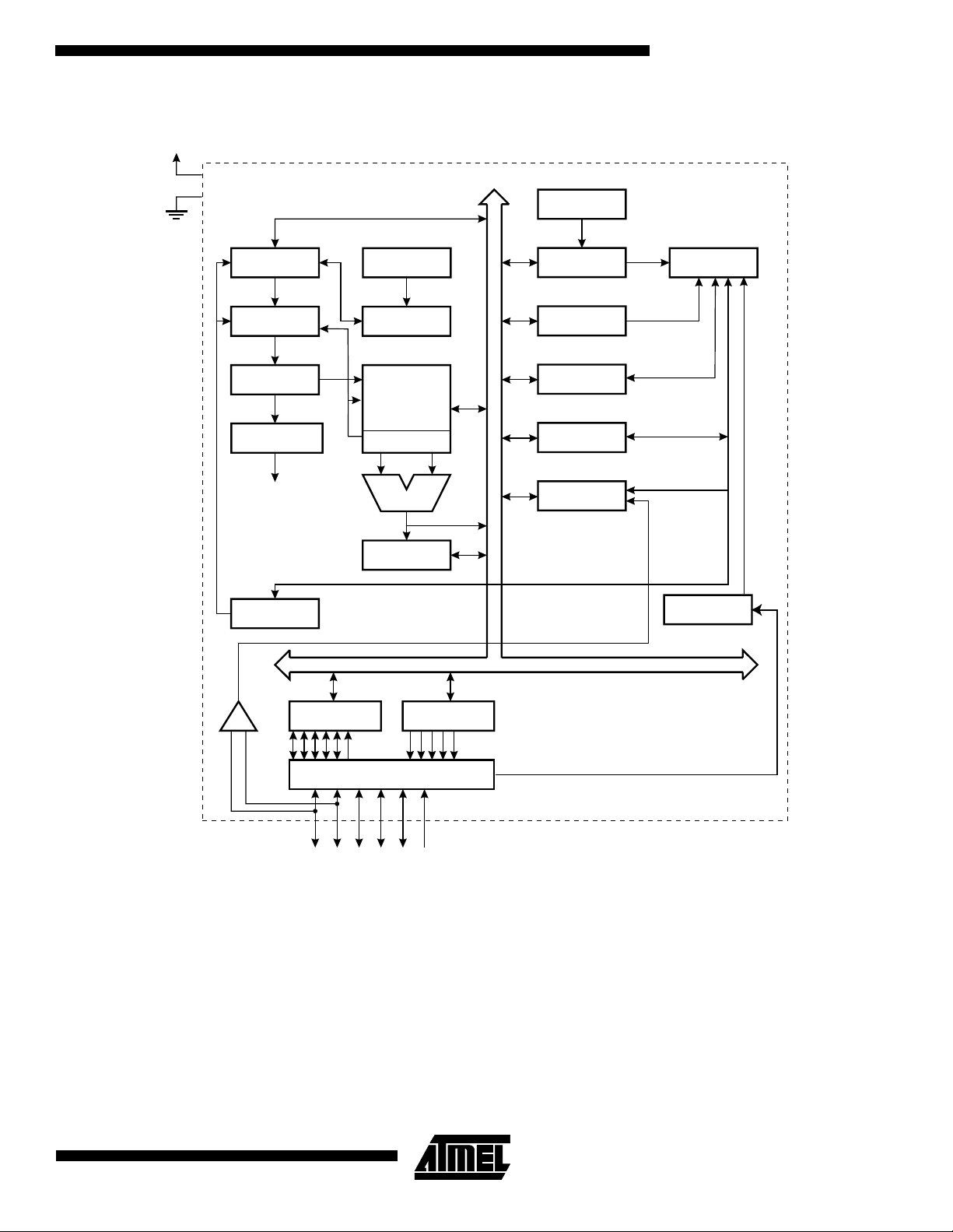
Figure 1. The ATtiny10/11 Block Diagram
VCC
GND
8-BIT DATABUS
INTERNAL
OSCILLATOR
ATtiny10/11/12
PROGRAM
COUNTER
PROGRAM
FLASH
INSTRUCTION
REGISTER
INSTRUCTION
DECODER
CONTROL
LINES
PROGRAMMING
LOGIC
STACK
POINTER
HARDWARE
STACK
GENERALPURPOSE
REGISTERS
Z
ALU
STATUS
REGISTER
WATCHDOG
TIMER
MCU CONTROL
REGISTER
MCU STATUS
REGISTER
TIMER/
COUNTER
INTERRUPT
UNIT
TIMING AND
CONTROL
OSCILLATORS
DATA REGISTER
ARATOR
COMP
PORTB
PORTB DRIVERS
PB0-PB5
+
ANALOG
DATA DIR.
REG. PORTB
3
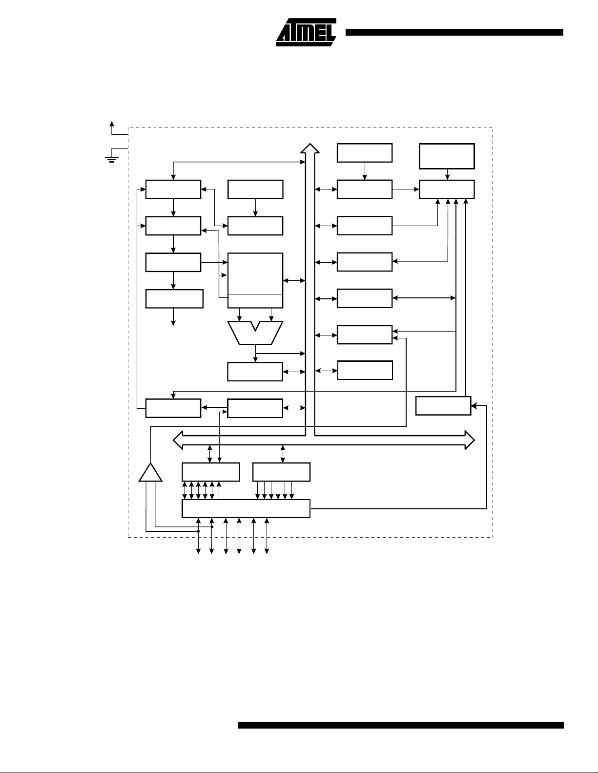
ATtiny12 Block Diagram
Figure 2. The ATtiny12 Block Diagram
VCC
GND
8-BIT DATA BUS
INTERNAL
OSCILLATOR
INTERNAL
CALIBRATED
OSCILLATOR
PROGRAM
COUNTER
PROGRAM
FLASH
INSTRUCTION
REGISTER
INSTRUCTION
DECODER
CONTROL
LINES
PROGRAMMING
LOGIC
ANALOG
DATA REGISTER
ARATOR
COMP
+
PORTB
PORTB DRIVERS
STACK
POINTER
HARDWARE
STACK
GENERALPURPOSE
REGISTERS
Z
ALU
STATUS
REGISTER
SPI
DATA DIR.
REG. PORTB
WATCHDOG
TIMER
MCU CONTROL
REGISTER
MCU STATUS
REGISTER
TIMER/
COUNTER
INTERRUPT
UNIT
EEPROM
TIMING AND
CONTROL
OSCILLATORS
PB0-PB5
The ATtiny12 provides the following features: 1K bytes of Flash, 64 bytes EEPROM, up to six general-purpose I/O lines,
32 general-purpose w orking regi sters, an 8-bit ti mer/counter , inter nal and ext ernal inter rupts, programma ble Watchdo g
Timer with internal oscillator, and two software-selectable power-saving modes. The Idle Mode stops the CPU while allowing the timer/counters and interrupt system to continue functioning. The Power-down Mode saves the register contents but
freezes the oscill ator, disa bling al l other chip fu nctions until the nex t interru pt or hardwa re reset. The wake-u p or interrup t
on pin change feature s enable the ATt iny12 to be highl y responsi ve to external eve nts, still feat uring the lowes t power
consumption while in the power-down modes.
4
ATtiny10/11/12

ATtiny10/11/12
The device is manufactured using Atmel’s high-density no nvolati le memory tec hnology. By combining an RISC 8-b it CPU
with Flash on a monolithic chip, the Atmel ATtiny12 is a powerful microcontroller that provides a highly-flexible and costeffective solution to many embedded control applications.
The ATtiny12 AVR is supported with a full suite of program and system development tools including: macro assemblers,
program debugger/simulators, in-circuit emulators, and evaluation kits.
Pin Descriptions
VCC
Supply voltage pin.
GND
Ground pin.
Port B (PB5..PB0)
Port B is a 6-bit I/O port. PB4..0 are I/O pins that can provide internal pull-ups (selected for each bit). On ATtiny10/11, PB5
is input only. On ATtiny12, PB5 is input or open-dr ain output. The port pi ns are tri-st ated when a reset con dition beco mes
active, even if the c lock is no t runn in g. T he us e of pi ns PB5..3 as input or I/O pins is lim ited , de pen din g on r es et a nd c lock
settings, as shown below.
Table 2. PB5..PB3 Functionality vs. Device Clocking Options
Device Clocking Option PB5 PB4 PB3
External Reset Enabled Used
External Reset Disabled Input
External Crystal - Used Used
External Low-frequency Crystal - Used Used
External Ceramic Resonator - Used Used
External RC Oscillator - I/O
External Clock - I/O Used
Internal RC Oscillator - I/O I/O
Notes: 1. “Used” means the pin is used for reset or clock purposes.
2. “-” means the pin function is unaffected by the option.
3. Input means the pin is a port input pin.
4. On ATtiny10/11, PB5 is input only. On ATtiny12, PB5 is input or open-drain output.
5. I/O means the pin is a port input/output pin.
(1)
(3)
(4)
/I/O
(2)
-
--
(5)
Used
XTAL1
Input to the inverting oscillator amplifier and input to the internal clock operating circuit.
XTAL2
Output from the inverting oscillator amplifier.
-
RESET
Reset input. An exter nal res et is gen er ate d by a lo w le ve l o n th e RE S ET p in. Reset p ul se s lon ger th an 50 ns will generate
a reset, even if the clock is not running. Shorter pulses are not guaranteed to generate a reset.
5
Clock Options
The device has the following clock source options, selectable by Flash fuse bits as shown:
Table 3. Device Clocking Options Select
Device Clocking Option ATtiny10/11 CKSEL2..0 ATtiny12 CKSEL3..0
External Crystal/Ceramic Resonator 111 1111 - 1010
External Low-frequency Crystal 110 1001 - 1000
External RC Oscillator 101 0111 - 0101
Internal RC Oscillator 100 0100 - 0010
External Clock 000 0001 - 0000
Reserved Other Options -
Note: “1” means unprogrammed, “0” means programmed.
The various choice s for each clo cking optio n give diff erent start -up times as shown in Tab le 7 on page 18 and Tabl e 9 on
page 19.
Internal RC Oscillator
The internal RC o scill ator option is an on -chip oscil lator r unnin g at a fix ed freq uen cy of 1 M Hz. If sel ected, the d evice can
operate with no external components. The device is shipped with this option selected. On ATtiny10/11, the Watchdog
Oscillator is used as a clock, while ATtiny12 uses a separate calibrated oscillator.
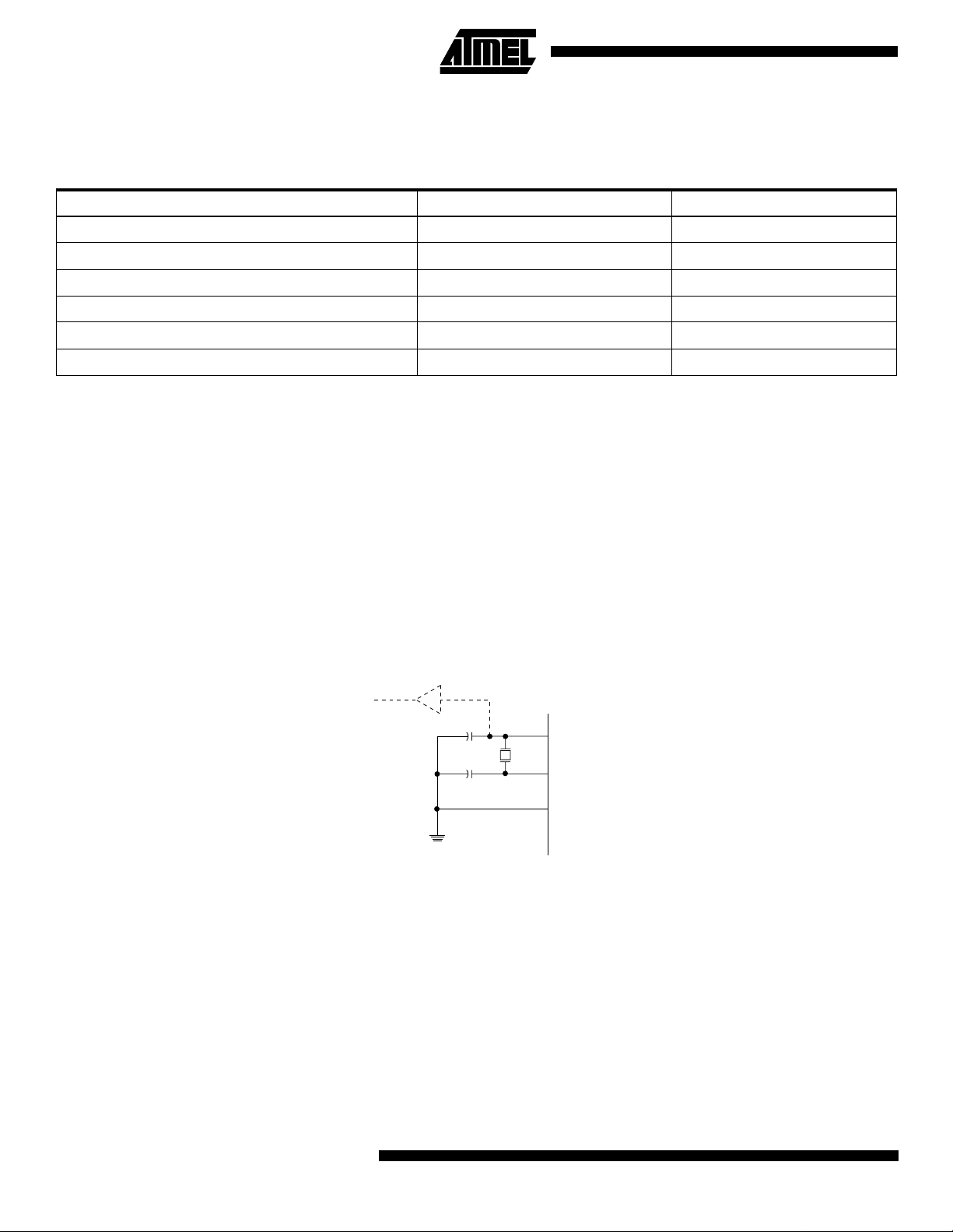
Crystal Oscillator
XTAL1 and XTAL2 are input and output, respectively, of an inverting amplifier which can be configured for use as an
on-chip oscillator, as shown in Figure 3. Either a quartz crystal or a ceramic resonator may be used.
Figure 3. Oscillator Connections
MAX 1 HC BUFFER
HC
C2
C1
Note: When using the MCU Oscillator as a clock for an external device, an HC buffer should be connected as indicated in the figure.
XTAL2
XTAL1
GND
6
ATtiny10/11/12

ATtiny10/11/12
External Clock
To drive the device from an external clock source, XTAL1 should be driven as shown in Figure 4.
Figure 4. External Clock Drive Configuration
PB4 (XTAL2)
EXTERNAL
OSCILLATOR
SIGNAL
External RC Oscillator
For timing insensitive applicati ons, the exter nal RC conf iguration sho wn in Figur e 5 can be used. For details on how to
choose R and C, see Table 29 on page 53.
XTAL1
GND
Figure 5. External RC Configuration
VCC
R
C
PB4 (XTAL2)
XTAL1
GND
Architectural Overview
The fast-access register file concept contains 32 x 8-bit general-purpose working registers with a single-clock-cycle access
time. This means th at d urin g on e s in gl e cloc k cyc le, one ALU (Arithmetic Logic Uni t) op erati on i s exec ute d. T wo ope ra nds
are output from the register file, the operation is executed, and the result is stored back in the register file – in one clock
cycle.
Two of the 32 registers can be used as a 16-bit pointer for indirect memory access. This pointer is called the Z-pointer, and
can address the register file and the Flash program memory.
The ALU supports arithmetic and logic functions between registers or between a constant and a register. Single-register
operations are als o executed in the ALU. F igure 2 sh ows the ATtiny 10/11/1 2 AVR RISC microco ntroller ar chitect ure. The
AVR uses a Harvard architecture concept with separate memories and buses for program and data memories. The program memory is a ccesse d with a two-sta ge pipeli ning. Wh ile o ne ins truc tion i s being exec uted, the next instr uction is pr efetched from the program memory. This con cept enables ins tructions to be exec uted in every clock cycle. The progr am
memory is reprogrammable Flash memory.
With the relative jump and relative call instructions, the whole 512 address space is directly accessed. All AVR instructions
have a single 16-bit word format, meaning that every program memory address contains a single 16-bit instruction.
7
During interrupts and subroutine calls, the return address program counter (PC) is stored on the stack. The stack is a
3-level-deep hardware stack dedicated for subroutines and interrupts.
The I/O memory space c ontain s 64 add resses for CPU per iphe ral func tions a s con trol reg isters , timer /count ers, a nd other
I/O functions. The memory spaces in the AVR architecture are all linear and regular memory maps.
Figure 6. The ATtiny10/11/12 AVR RISC Architecture
8-bit Data Bus
512 x 16
Program
Flash
Instruction
Register
Instruction
Decoder
Control Lines
Program
Counter
Direct Addressing
Status
and Test
32 x 8
General-
purpose
Registers
ALU
64 x 8 EEPROM
(ATtiny12 only)
Control
Registers
Interrupt
Unit
SPI Unit
(ATtiny12 only)
8-bit
Timer/Counter
Watchdog
Timer
Analog
Comparator
6
I/O Lines
A flexible interrupt module has its control registers in the I/O space with an additional global interrupt enable bit in the status
register. All the different interrupts have a separate interrupt vector in the interrupt vector table at the beginning of the
program memory. The di fferent interrup ts hav e prior ity in acco rdance with th eir inte rrupt v ector p osition. The lower the
interrupt vector address, the higher the priority.
8
ATtiny10/11/12

General-purpose Register File
Figure 7 shows the structure of the 32 general-purpose registers in the CPU.
ATtiny10/11/12
Figure 7. AVR
CPU General-purpose Working Registers
70
R0
R1
R2
General- …
purpose …
Working R28
Registers R29
R30 (Z-register low byte)
R31 (Z-register high byte)
All the register operating instructions in the instruction set have direct- and single-cycle access to all registers. The only
exception is the f iv e con sta nt ar ith meti c an d logi c in st ru cti on s SB CI, SUB I, CPI, ANDI, and ORI between a constant and a
register and the LDI instructi on for load- immediat e constant data. Th ese instruc tions apply to the se cond half of the r egisters in the register file – R16..R31. The general SBC, SUB, CP, AND, OR and all other operations between two registers or
on a single register apply to the entire register file.
Registers 30 and 31 form a 16-bi t pointer (th e Z-pointer ) which is used fo r indirect Flash mem ory and regist er file acces s.
When the register file is accessed, the contents of R31 are discarded by the CPU.
ALU – Arithmetic Logic Unit
The high-performan ce AVR AL U operat es in direct con nectio n with all the 32 general- purpose working r egisters. W ithin a
single clock cy cl e, AL U ope r atio ns be tween r egi ster s in the re gis te r f ile ar e ex ec uted . The ALU operations are divi ded in to
three main categories – arithmetic, logic and bit-functions. Some microcontrollers in the AVR product family feature a hardware multiplier in the arithmetic part of the ALU.
Flash Program Memory
The ATtiny10/11/12 contains 1K bytes on-chip Flash memory for program storage. Since all instructions are single 16-bit
words, the Flash is organized as 512 x 16 words. The Flash memory has an endurance of at least 1000 write/erase cycles.
The ATtiny10/11/12 Program Counter is 9 bits wide, thus addressing the 512 words Flash program memory.
See page 39 for a detailed description on Flash memory programming.
Program and Data Addressing Modes
The ATtiny10/11/12 AVR RISC Microcontroller supports powerful and efficient addressing modes. This section describes
the different addressing modes supported in the ATtiny10/11/12. In the figures, OP means the operation code part of the
instruction word. To simplify, not all figures show the exact location of the addressing bits.
9

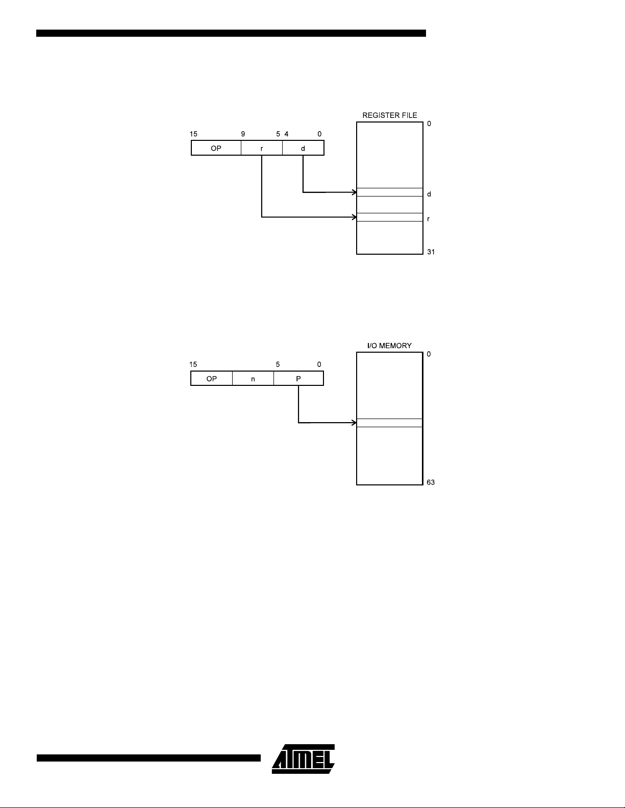
Register Direct, Single Register Rd
Figure 8. Direct Single-register Addressing
The operand is contained in register d (Rd).
Register Indirect
Figure 9. Indirect Register Addressing
REGISTER FILE
Z-register
The register accessed is the one pointed to by the Z-register (R31, R30).
0
30
31
10
ATtiny10/11/12
ATtiny10/11/12
Register Direct, Two Registers Rd and Rr
Figure 10. Direct Register Addressing, Two Registers
Operands are contained in register r (Rr) and d (Rd). The result is stored in register d (Rd).
I/O Direct
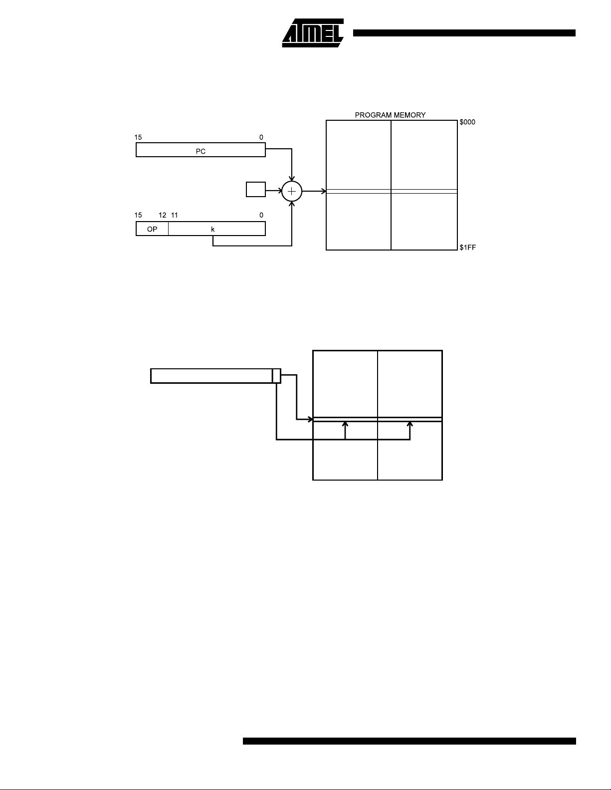
Figure 11. I/O Direct Addressing
Operand address is contained in 6 bits of the instruction word. n is the destination or source register address.
11
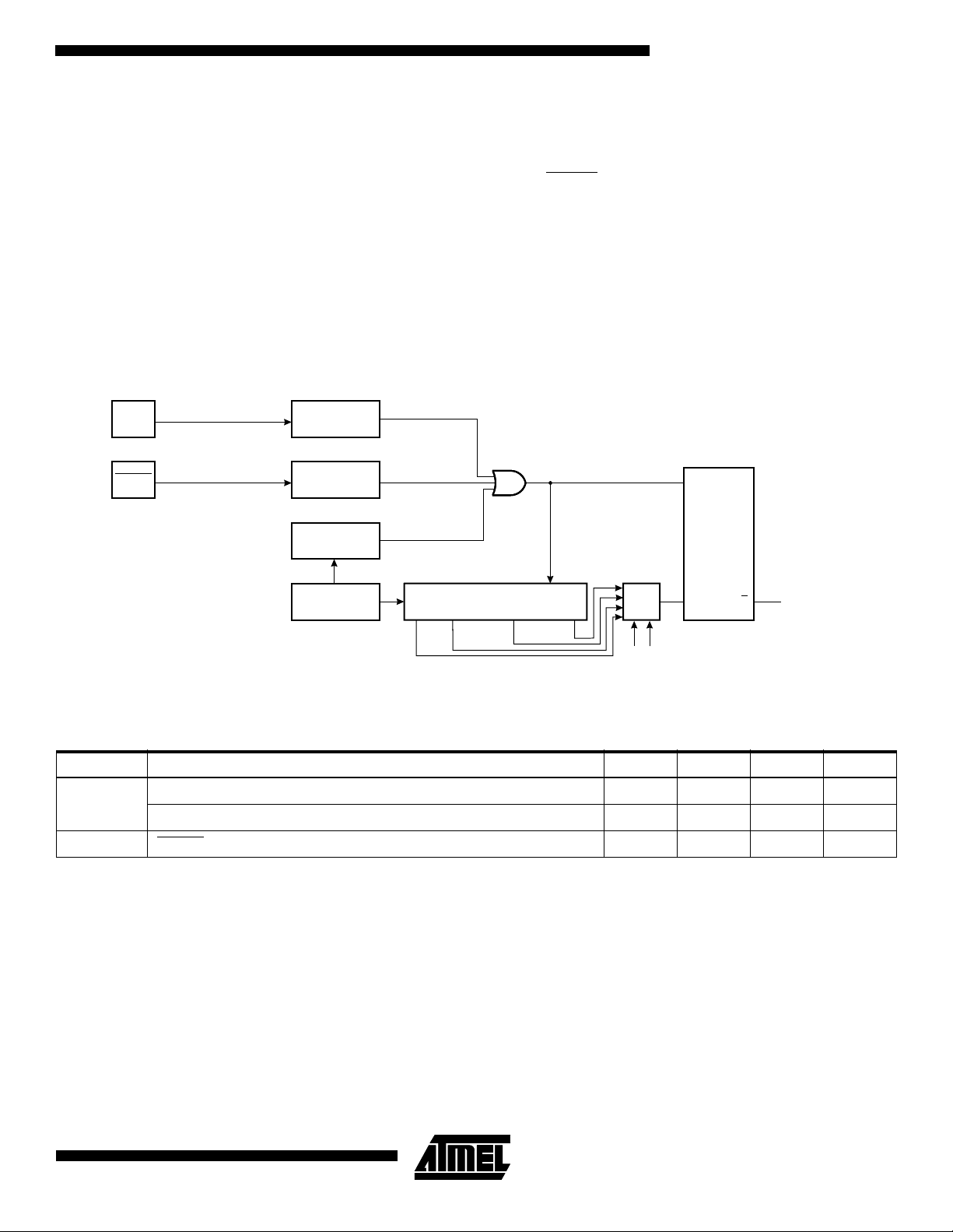
Relative Program Addressing, RJMP and RCALL
Figure 12. Relative Program Memory Addressing
+1
Program execution continues at address PC + k + 1. The relative address k is -2048 to 2047.
Constant Addressing Using the LPM Instruction
Figure 13. Code Memory Constant Addressing
PROGRAM MEMORY
15 1 0
Z-REGISTER
$000
$1FF
Constant byte address is specified by the Z-register contents. The 15 MSBs select word address (0 - 511), the LSB selects
low byte if cleared (LSB = 0) or high byte if set (LSB = 1).
Subroutine and Interrupt Hardware Stack
The ATtiny10/11 /12 uses a 3 -le vel-d eep hardw are stac k f or su brou tines and inter rup ts. The ha rdwa re sta ck is 9 bi ts w ide
and stores the program counter (PC) return address while subroutines and interrupts are executed.
RCALL instructions and interrupts push the PC return address onto stack level 0, and the data in the other stack levels 1-2
are pushed one level deeper in the stack. When a RET or RETI instruction is executed the returning PC is fetched from
stack level 0, and the data in the other stack levels 1-2 are popped one level in the stack.
If more than three subsequent su brouti ne calls or interrupt s are exec uted, the fi rst valu es written to the stack are overwr itten. Pushing four ret urn ad dr es ses A 1, A 2, A3 a nd A 4, fo ll owed by fou r sub ro utine or interrupt returns, will pop A 4, A3, A 2
and once more A2 from the hardware stack.
12
ATtiny10/11/12

ATtiny10/11/12
EEPROM Data Memory
The ATtiny12 contains 64 b yte s o f data EE PRO M m emo ry . It is o rg ani ze d as a sepa ra te da ta sp ac e, i n whi ch singl e by tes
can be read and written. The EEPROM has an endur ance of at least 100, 000 write /erase cy cles. The acces s betwee n the
EEPROM and the CPU is de scrib ed on pag e 33, sp ecifyin g the EE PROM Addres s Regis ter, th e EEPRO M Data Reg ister ,
and the EEPROM Control Register.
For SPI data downloading, see “Memory Programming ” on page 39 for a detailed description.
Memory Access and Instruction Execution Timing
This section describes the general access timing concepts for instruction execution and internal memory access.
The AVR CPU is driven by the System Clock Ø, directly generated from the external clock c rystal for the c hip. No interna l
clock division is used.
Figure 14 shows the parallel instruction fetches and instructio n executions enabled by the Harvard architecture and the
fast-access register file concept. This is the basic pipelining concept to obtain up to 1 MIPS per MHz with the corresponding
unique results for functions per cost, functions per clocks, and functions per power-unit.
Figure 14. The Parallel Instruction Fetches and Instruction Executions
T1 T2 T3 T4
System Clock Ø
1st Instruction Fetch
1st Instruction Execute
2nd Instruction Fetch
2nd Instruction Execute
3rd Instruction Fetch
3rd Instruction Execute
4th Instruction Fetch
Figure 15 shows the internal timing concept for the register file. In a single clock cycle, an ALU operation using two register
operands is executed and the result is stored back to the destination register.
Figure 15. Single-cycle ALU Operation
T1 T2 T3 T4
System Clock Ø
Total Execution Time
Register Operands Fetch
ALU Operation Execute
Result Write Back
13

I/O Memory
The I/O space definition of the ATtiny10/11/12 is shown in the following table:
Table 4. ATtiny10/11/12 I/O Space
Address Hex Name Device Function
$3F SREG ATtiny10/11/12 Status Register
$3B GIMSK ATtiny10/11/12 General Interrupt Mask Register
$3A GIFR ATtiny10/11/12 General Interrupt Flag Register
$39 TIMSK ATtiny10/11/12 Timer/Counter Interrupt Mask Register
$38 TIFR ATtiny10/11/12 Timer/Counter Interrupt Flag Register
$35 MCUCR ATtiny10/11/12 MCU Control Register
$34 MCUSR ATtiny10/11/12 MCU Status Register
$33 TCCR0 ATtiny10/11/12 Timer/Counter0 Control Register
$32 TCNT0 ATtiny10/11/12 Timer/Counter0 (8-bit)
$31 OSCCAL ATtiny12 Oscillator Calibration Register
$21 WDTCR ATtiny10/11/12 Watchdog Timer Control Register
$1E EEAR ATtiny12 EEPROM Address Register
$1D EEDR ATtiny12 EEPROM Data Register
$1C EECR ATtiny12 EEPROM Control Register
$18 PORTB ATtiny10/11/12 Data Register, Port B
$17 DDRB ATtiny10/11/12 Data Direction Register, Port B
$16 PINB ATtiny10/11/12 Input Pins, Port B
$08 ACSR ATtiny10/11/12 Analog Comparator Control and Status Register
Note: Reserved and unused locations are not shown in the table.
All the different ATtiny10/11/12 I/O and peripherals are placed in the I/O space. The different I/O locations are accessed by
the IN and OUT instructions transferring data between the 32 general-purpose working registers and the I/O space. I/O registers within the addr ess ran ge $00 - $1F ar e direc tly b it-acces sible us ing th e SBI and CBI instruc tions . In these regis ters,
the value of sing le bits can be checked by using the SBIS and SBIC inst ruct ions. Refer to the Instruct ion Se t S umm ar y for
more details.
For compatibility wi th fu tur e de vi ce s, re se rv ed bit s s ho uld be wr i tten to z ero i f ac ce ss ed . Res er v ed I/ O m emo ry ad dr es se d
should never be written.
The different I/O and peripherals control registers are explained in the following sections.
Status Register – SREG
The AVR status register (SREG) at I/O space location $3F is defined as:
Bit 76543210
$3F I T H S V N Z C SREG
Read/Write R/W R/W R/W R/W R/W R/W R/W R/W
Initial value 0 0 0 0 0 0 0 0
Bit 7 - I: Global Interrupt Enable
•
The global interrup t enable bit must be set (one) for the interrup ts to be enable d. The indivi dual inter rupt enab le control is
then performed in sep arate contr ol registe rs. If the gl obal interru pt enable r egister is cleared (ze ro), none of the interrupts
14
ATtiny10/11/12

ATtiny10/11/12
are enabled independent of the individual interrupt enable settings. The I-bit is cleared by hardware after an interrupt has
occurred, and is set by the RETI instruction to enable subsequent interrupts.
Bit 6 - T: Bit Copy Storage
•
The bit copy instruc tions B LD (Bit L oaD) a nd BST (Bit ST ore) u se the T-bit a s sour ce and destinati on for the op erated bi t.
A bit from a register in the registe r file ca n be co pied into T by the BST instruction, and a bit in T can be cop ied into a bi t in
a register in the register file by the BLD instruction.
Bit 5 - H: Half Carry Flag
•
The half carry flag H indicates a half-carry in some arithmetic operations. See the Instruction Set description for detailed
information.
Bit 4 - S: Sign Bit, S = N ⊕ V
•
The S-bit is always an exclusive or between the negative flag N and the two’s complement overflow flag V. See the Instruction Set description for detailed information.
•
Bit 3 - V: Two’s Complement Overflow Flag
The two’s complement overflow flag V supports two’s com plement arithmetic. S ee the Instruction S et description for
detailed information.
•
Bit 2 - N: Negative Flag
The negative flag N indicates a negative result from an arithmetical or logical operation. See the Instruction Set description
for detailed information.
Bit 1 - Z: Zero Flag
•
The zero flag Z indicates a zero result from an arithmetical or logical operation. See the Instruction Set description for
detailed information.
Bit 0 - C: Carry Flag
•
The carry flag C indicates a carry in an a rithmetical or logical ope ration. See the Ins truction Set des cription for d etailed
information.
Note that the status register is not automatically stored when entering an interrupt routine and restored when returning from
an interrupt routine. This must be handled by software.
Reset and Interrupt Handling
The ATtiny10/11 provides four different interrupt sources and the ATtiny12 provides five. These interrupts and the separate
reset vector each hav e a se par at e pr ogram vector in the program memory spac e. A ll t he in terr upts are as si gn ed in div i dua l
enable bits which must be set (one) together with the I-bit in the status register in order to enable the interrupt.
The lowest addresses i n the pro gram memo ry space are automatica lly defined a s the Rese t and Inter rupt vector s. The
complete list of vectors is shown in Table 5. The list also determines the priority levels of the different interrupts. The lower
the address, the higher the priority level. RESET has the highest priority, and next is INT0 – the External Interrupt Request
0, etc.
15

Table 5. Reset and Interrupt Vectors
Vector No. Device Program Address Source Interrupt Definition
1 ATtiny10/11 $000 RESET
External Pin, Power-on Reset and
Watchdog Reset
1 ATtiny12 $000 RESET
External Pin, Power-on Reset, Brown-out
Reset and Watchdog Reset
2 ATtiny10/11/12 $001 INT0 External Interrupt Request 0
3 ATtiny10/11/12 $002 I/O Pins Pin Change Interrupt
4 ATtiny10/11/12 $003 TIMER0, OVF0 Timer/Counter0 Overflow
5 ATtiny10/11 $004 ANA_COMP Analog Comparator
5 ATtiny12 $004 EE_RDY EEPROM Ready
6 ATtiny12 $005 ANA_COMP Analog Comparator
The most typical and general program setup for the reset and interrupt vector addresses for the ATtiny10/11 are:
Address Labels Code Comments
$000 rjmp RESET ; Reset handler
$001 rjmp EXT_INT0 ; IRQ0 handler
$002 rjmp PIN_CHANGE ; Pin change handler
$003 rjmp TIM0_OVF ; Timer0 overflow handler
$004 rjmp ANA_COMP ; Analog Comparator handler
;
$005 MAIN: <instr> xxx ; Main program start
… … … …
The most typical and general program setup for the reset and interrupt vector addresses for the ATtiny12 are:
Address Labels Code Comments
$000 rjmp RESET ; Reset handler
$001 rjmp EXT_INT0 ; IRQ0 handler
$002 rjmp PIN_CHANGE ; Pin change handler
$003 rjmp TIM0_OVF ; Timer0 overflow handler
$004 rjmp EE_RDY ; EEPROM Ready handler
$005 rjmp ANA_COMP ; Analog Comparator handler
;
$006 MAIN: <instr> xxx ; Main program start
… … … …
16
ATtiny10/11/12
ATtiny10/11/12
Reset Sources
The ATtiny10/11/12 provides three or four sources of reset:
• Power-on Reset. The MCU is reset when the supply voltage is below the power-on reset threshold (V
• External Reset. The MCU is reset when a low level is present on the RESET pin for more than 50 ns.
• Watchdog Reset. The MCU is reset when the Watchdog timer period expires and the Watchdog is enabled.
• Brown-out Reset. The MCU is reset when the supply voltage V
falls below a certain voltage (ATtiny12 only).
CC
During reset, all I/O regist ers are the n set to their ini tial valu es, and the pro gram starts execution from address $000. The
instruction pla ced in addr ess $000 m ust be an RJM P – relat ive ju mp – ins tructi on to the rese t han dling routi ne. If the program never enables an interrupt sour ce, the interrupt v ectors are not used, a nd regular progr am code can be pl aced at
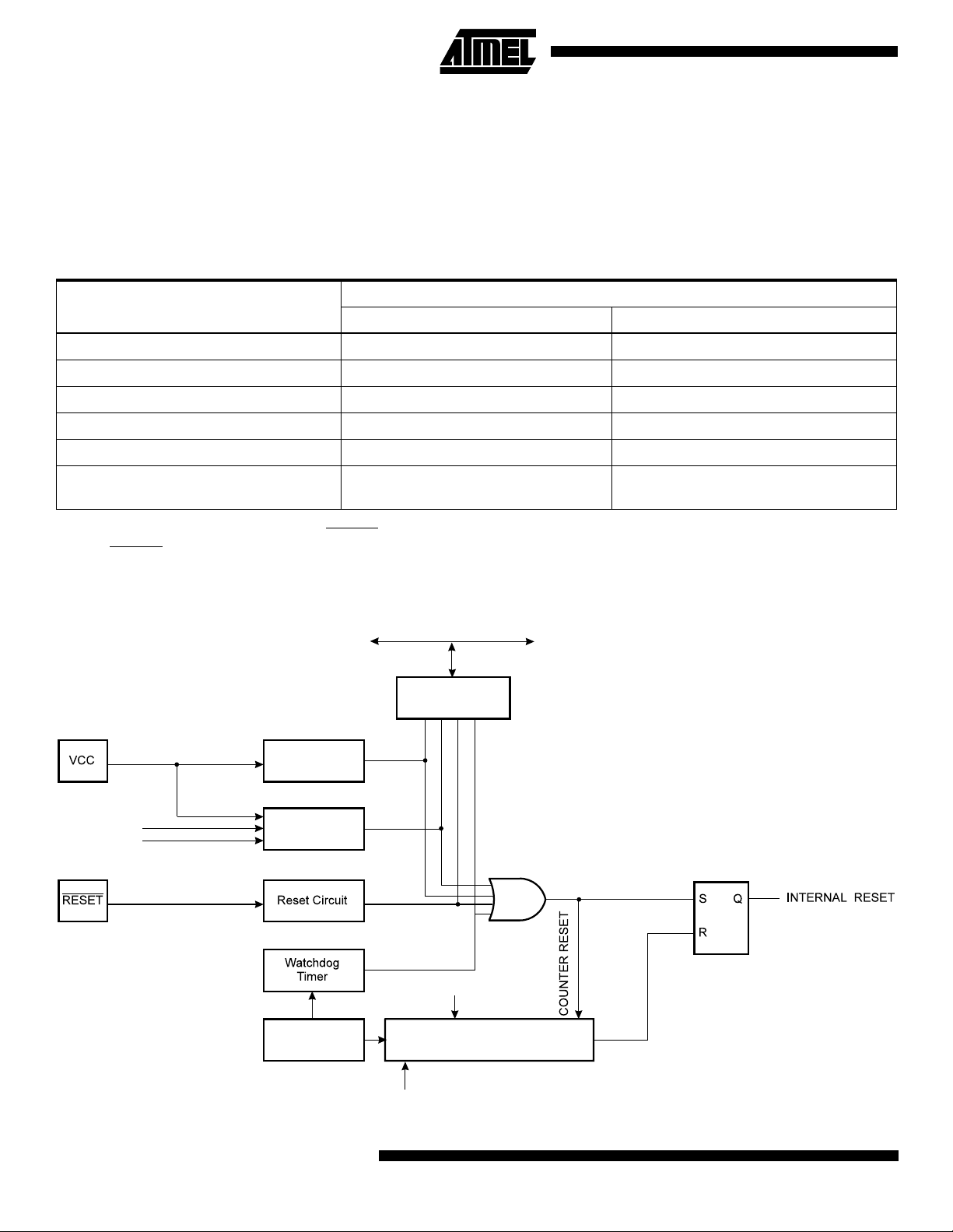
these locations. The circuit diagram in Figure 16 shows the reset logic for the ATtiny10/11. Figure 17 shows the reset logic
for the ATtiny12. Table 6 def ine s th e el ec tric al param eter s of the reset circuitry for ATtiny10/11. T ab le 8 sh ows the p ar ameters of the reset circuitry for ATtiny12.
Figure 16. Reset Logic for the ATtiny10/11
VCC
Power-on Reset
Circuit
POR
POT
).
RESET
Reset Circuit
Watchdog
Timer
On-chip
RC Oscillator
COUNTER RESET
20-stage Ripple Counter
Q3 Q19
Q9
Q13
CKSEL
FSTRT
QS
INTERNAL
R
Q
RESET
Table 6. Reset Characteristics for the ATtiny10/11
Symbol Parameter Min Typ Max Units
(1)
V
POT
V
RST
Note: 1. The Power-on Reset will not work unless the supply voltage has been below V
Power-on Reset Threshold Voltage (rising) 1.0 1.4 1.8 V
Power-on Reset Threshold Voltage (falling) 0.4 0.6 0.8 V
RESET Pin Threshold Voltage 0.6 V
(falling).
POT
CC
V
17
Power-on Reset for the ATtiny10/11
A Power-on Reset (POR) circuit ensures that the device is reset from power-on. As shown in Figure 16, an internal timer is
clocked from the watchdog timer. Thi s timer prevents the MCU from starting a cer tain period after V
Power-on Threshold Voltage – V
. See Figure 18. The total reset period is the Delay Time-out period – t
POT
has reached the
CC
. The FSTRT
TOUT
fuse bit in the Flash can be programmed to give a shorter start-up time.The start-up times for the different clock options are
shown in the follo wing ta ble. T he Wa tchdog Oscill ator i s used for t iming the st art-up time, a nd t his osc illator is voltag e
dependent as shown in the section “ATtiny11 Typical Characteristics” on page 54.
Table 7. Start-up Times for the ATtiny10/11 (V
Selected Clock Option
= 2.7V)
CC
Start-up Time t
TOUT
FSTRT Unprogrammed FSTRT Programmed
External Crystal 67 ms 4.2 ms
External Ceramic Resonator 67 ms 4.2 ms
External Low-frequency Crystal 4.2 s 4.2 s
External RC Oscillator 4.2 ms 67 µs
Internal RC Oscillator 4.2 ms 67 µs
External Clock 4.2 ms
If the built-in start-up delay is sufficient, RESET
ing the RESET
pin low for a period after VCC has been applied, the Power-on Reset period can be extended. Refer to
can be connected to VCC directly or via an external pull-up resistor. By hold-
5 clocks from reset,
2 clocks from powe r-down
Figure 19 for a timing example on this.
Figure 17. Reset Logic for the ATtiny12
DATA BUS
MCU Status
Register (MCUSR)
BODEN
BODLEVEL
18
Power-on Reset
Circuit
Brown-out
Reset Circuit
On-chip
RC Oscillator
ATtiny10/11/12
CK
BORF
PORF
CKSEL[3:0]
WDRF
EXTRF
Delay Counters
Full

ATtiny10/11/12
Table 8. Reset Characteristics for the ATtiny12
Symbol Parameter Condition Min Typ Max Units
Power-on Reset Threshold Voltage
(1)
V
POT
(rising)
Power-on Reset Threshold Voltage
(falling)
BOD disabled 1.0 1.4 1.8 V
BOD enabled 0.6 1.2 1.8 V
BOD disabled 0.4 0.6 0.8 V
BOD enabled 0.6 1.2 1.8 V
V
RST
RESET Pin Threshold Voltage 0.6V
CC
(BODLEVEL = 1) 1.7 1.8 1.9
V
BOT
Note: 1. The Power-on Reset will not work unless the supply voltage has been below V
Brown-out Reset Threshold Voltage
(BODLEVEL = 0) 2.6 2.7 2.8
(falling).
POT
Table 9. ATtiny12 Clock Options and Start-up Times
Start-up Time, V
CKSEL3..0 Clock Source
1111 Ext. Crystal/Ceramic Resonator
1110 Ext. Crystal/Ceramic Resonator
1101 Ext. Crystal/Ceramic Resonator
(1)
(1)
(1)
BODLEVEL Unprogrammed
3.6 ms + 1K CK 4.2 ms + 1K CK
1100 Ext. Crystal/Ceramic Resonator 16K CK 16K CK
1011 Ext. Crystal/Ceramic Resonator 3.6 ms + 16K CK 4.2 ms + 16K CK
1010 Ext. Crystal/Ceramic Resonator 57 ms + 16K CK 67 ms + 16K CK
1001 Ext. Low-frequency Crystal 57 ms + 1K CK 67 ms + 1K CK
1000 Ext. Low-frequency Crystal 57 ms + 32K CK 67 ms + 32K CK
0111 Ext. RC Oscillator 6 CK 6 CK
0110 Ext. RC Oscillator 3.6 ms + 6 CK 4.2 ms + 6 CK
= 1.8V,
CC
Start-up Time, VCC = 2.7V,
BODLEVEL Programmed
1K CK 1K CK
57 ms 1K CK 67 ms + 1K CK
V
V
0101 Ext. RC Oscillator 57 ms + 6 CK 67 ms + 6 CK
0100 Int. RC Oscillator 6 CK 6 CK
0011 Int. RC Oscillator 3.6 ms + 6 CK 4.2 ms + 6 CK
0010 Int. RC Oscillator 57 ms + 6 CK 67 ms + 6 CK
0001 Ext. Clock 6 CK 6 CK
0000 Ext. Clock 3.6 ms + 6 CK 4.2 ms + 6 CK
Note: 1. Due to the limited number of clock cycles in the start-up period, it is recommended that Ceramic Resonator be used.
This table shows the start-up times from reset. From sleep, only the clock counting part of the start-up time is used. The
Watchdog oscillator is used for ti min g th e r eal -tim e part of the start-up time. Th e nu mbe r of WD T os ci ll ato r cy c les us ed for
each time-out is shown in Table 10.
19

Table 10. Number of Watchdog Oscillator Cycles
BODLEVEL Time-out Number of Cycles
Unprogrammed 3.6 ms (at V
Unprogrammed 57 ms (at V
Programmed 4.2 ms (at V
= 1.8V) 256
cc
= 1.8V) 4K
cc
= 2.7V) 1K
cc
Programmed 67 ms (at Vcc = 2.7V) 16K
The frequency of the watch dog osc illator is voltag e depe ndent as shown in the sect ion “A Ttiny 11 T ypic al Chara cter ist ics”
on page 54.
Note that the BODLEVEL fuse c an be us ed to s elec t st ar t- up times ev en i f the Brown- o ut Dete ct ion is dis ab led (by l eav in g
the BODEN fuse unprogrammed).
The device is shipped with CKSEL3..0 = 0010.
Power-on Reset for the ATtiny12
A Power-on Reset (POR) pulse is generated by an on-ch ip detection circuit. The de tection level is nominally 1.4V. The
POR is activated whenever V
is below the detection level. The POR circuit can be used to trigger the start-up reset, as
CC
well as detect a failure in supply voltage.
The Power-on Reset (POR) circuit ensures that the device is reset from power-on. Reaching the Power-on Reset threshold
voltage invokes a de la y c oun ter , wh ic h de ter mi nes the delay for which the device is ke pt i n Re set after V
rise. The time-
CC
out period of the del ay cou nter can be defined by the user t hr ough the CKS EL fuses . T he dif fer ent se lec ti ons for th e de lay
period are presented in Table 9. The Reset signal is activated again, without any delay, when the V
decreases below
CC
detection level.
If the built-in start-up delay is sufficient, RESET
Figure 18. By holding the RESET
pin low for a period after VCC has been applied, the Power-on Reset period can be
can be connected to VCC directly or via an external pull-up resistor. See
extended. Refer to Figure 19 for a timing example on this.
Figure 18. MCU Start-up, RESET
V
CC
RESET
TIME-OUT
INTERNAL
RESET
Tied to VCC.
V
POT
V
RST
t
TOUT
20
ATtiny10/11/12

ATtiny10/11/12
Figure 19. MCU Start-up, RESET
V
CC
RESET
TIME-OUT
INTERNAL
RESET
Extended Externally
V
POT
V
RST
t
TOUT
External Reset
An external reset is generated by a low level on the RESET
pin. Reset pulses longer than 50 ns will generate a reset, even
if the clock is no t running. Shorter pu lses are n ot guarante ed to gener ate a re set. When the applied s ignal reac hes the
Reset Threshold Voltage – V
– on its positive edge, the delay timer starts the MCU after the Time-out period (t
RST
TOUT
) has
expired.
Figure 20. External Reset during Operation
V
CC
RESET
TIME-OUT
INTERNAL
RESET
V
RST
t
TOUT
Brown-out Detection (ATtiny12)
ATtiny12 has an on-chi p brown-out dete ction (BOD ) circuit for monit oring the V
circuit can be enabled/disabled by the fuse BODEN. When BODEN is enabled (BODEN programmed), and V
below the trigger level, the brown-out reset is immediately activated. When V
level during the opera tion. The BOD
CC
increases above the trigger level, the
CC
decreases
CC
brown-out reset is de ac tiv ate d af ter a d el ay. T he d el ay is de fin ed b y the u se r in the sa me w ay as the del ay of PO R sig nal ,
in Table 5. The trigger level for the BOD can be selected by the fuse BODLEVEL to be 1.8V (BODLEVEL unprogrammed),
or 2.7V (BODLEVEL programmed). The trigger level has a hysteresis of 50 mV to ensure spike-free brown-out detection.
The BOD circuit will only detect a drop in V
if the voltage stays below the trigger level for longer than 7 µs for trigger level
CC
2.7V, 24 µs for trigge r level 1.8V (typical values).
21
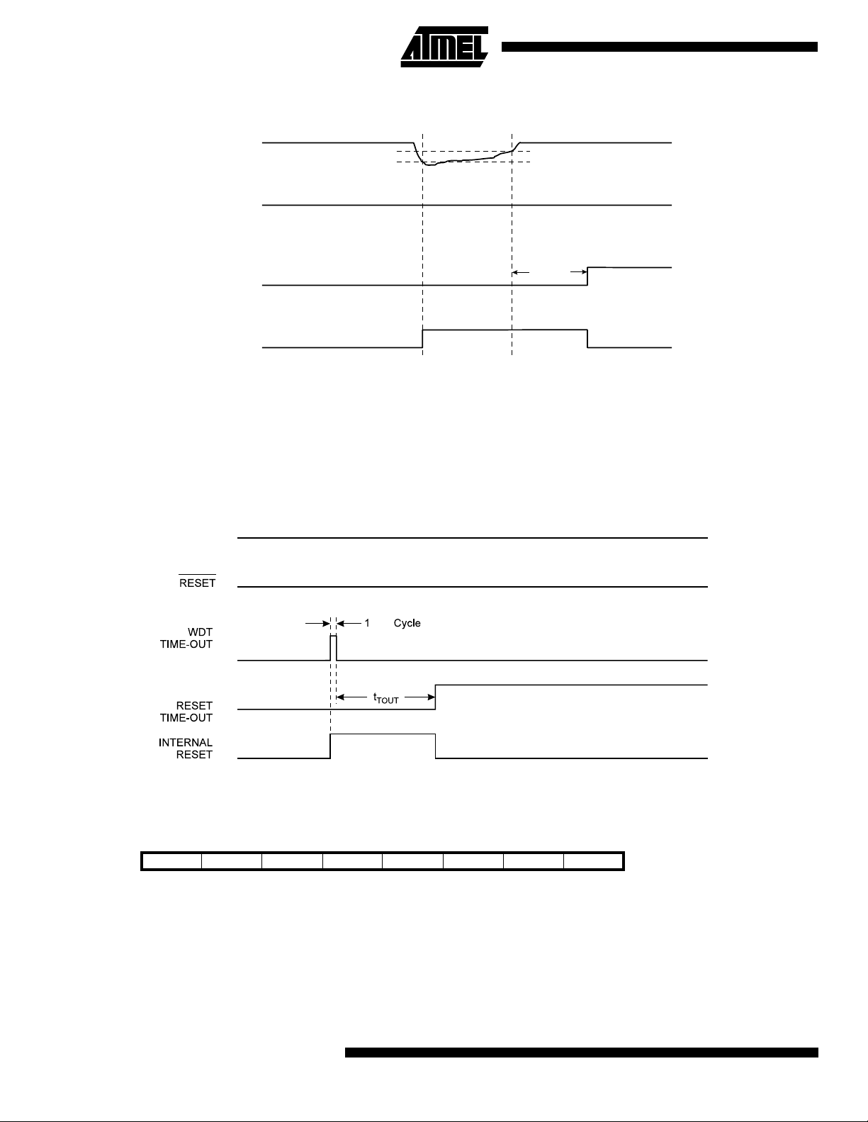
Figure 21. Brown-out Reset during Operation (ATtiny12)
V
CC
V
BOT-
V
BOT+
RESET
t
TIME-OUT
TOUT
INTERNAL
RESET
Note: The hy steresis on V
BOT
: V
BOT +
= V
+ 25 mV, V
BOT
BOT-
= V
BOT
- 25 mV.
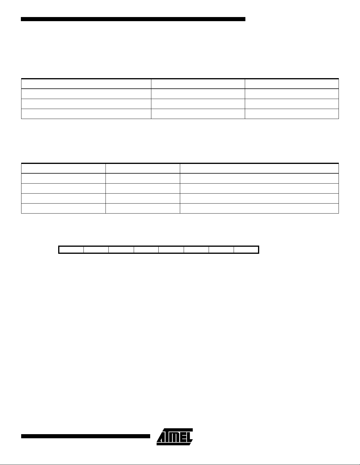
Watchdog Rese t
When the Watchdog tim es out , it wil l gene rate a s hor t res et pul se of 1 CK cy c le dur at ion . O n th e fa ll ing ed ge o f thi s pul s e,
the delay timer starts counting the Time-out period (t
). Refer to page 31 for details on operation of the Watchdog.
TOUT
Figure 22. Watchdog Reset during Operatio n
V
CC
CK
MCU Status Register – MCUSR of the ATtiny10/11
The MCU Status Register provides information on which reset source caused an MCU reset.
Bit 76543210
$34 ------EXTRFPORFMCUSR
Read/Write R R R R R R R/W R/W
Initial value 0 0 0 0 0 0 See bit description
Bit 7..2 - Res: Reserved Bits
•
These bits are reserved bits in the ATtiny10/11 and always read as zero.
Bit 1 - EXTRF: EXTernal Reset Flag
•
After a power-on reset, this bit is undefined (X). It will be set by an external reset. A watchdog reset will leave this bit
unchanged.
22
ATtiny10/11/12
ATtiny10/11/12
Bit 0 - PORF: Power-on Reset Flag
•
This bit is set by a power-on reset. A watchdog reset or an external reset will leave this bit unchanged.
To summarize, the following table shows the value of these two bits after the three modes of reset.
Table 11. PORF and EXTRF Values after Reset
Reset Source EXTRF PORF
Power-on undefined 1
External Reset 1 unchanged
Watchdog Reset unchanged unchanged
To identify a reset condition, the user software should clear both the PORF and EXTRF bits as early as possible in the program. Checking the PORF and EXTRF values is done before the bits are cleared. If the bit is cleared before an external or
watchdog reset occurs, the source of reset can be found by using the following truth table:
Table 12. Reset Source Identification
EXTRF PORF Reset Source
0 0 Watchdog Re set
1 0 External Reset
0 1 Power-on Reset
1 1 Power-on Reset
MCU Status Register – MCUSR for the ATtiny12
The MCU Status Register provides information on which reset source caused an MCU reset.
Bit 76543210
$34 - - - - WDRF BORF EXTRF PORF MCUSR
Read/Write R R R R R/W R/W R/W R/W
Initial value 0 0 0 0 See bit description
Bit 7..4 - Res: Reserved Bits
•
These bits are reserved bits in the ATtiny12 and always read as zero.
Bit 3 - WDRF: Watchdog Reset Flag
•
This bit is set if a watchdog reset occurs. The bit is reset by a power-on reset, or by writing a logic zero to the flag.
Bit 2 - BORF: Brown-out Reset Flag
•
This bit is set if a brown-out reset occurs. The bit is reset by a power-on reset, or by writing a logic zero to the flag.
•
Bit 1 - EXTRF: EXTernal Reset Flag
This bit is set if an external reset occurs. The bit is reset by a power-on reset, or by writing a logic zero to the flag.
Bit 0 - PORF: Power-on Reset Flag
•
This bit is set if a power-on reset occurs. The bit is reset by writing a logic zero to the flag.
To use the reset flags to iden tify a res et c ondi ti on, th e user sho ul d read an d the n re se t the MC USR as early as possible in
the program. If the re gister is c leared bef ore anot her reset oc curs, the source of th e reset ca n be found by examinin g the
reset flags.
ATtiny12 Interna l Voltage Reference
ATtiny12 features an internal voltage reference with a nominal voltage of 1.22V. This reference is used for Brown-out
Detection, and it can be used as an input to the Analog Comparator.
23

Voltage Reference Enable Signals and Start-up Time
The voltage reference has a start-up time that may influence the way it should be used. The maximum start-up time is TBD.
To save power, the reference is not always turned on. The reference is on during the following situations:
1. When BOD is enabled (by programming the BODEN fuse)
2. When the bandgap reference is connected to the Analog Comparator (by setting the AINBG bit in ACSR)
Thus, when BOD is not enabled, after setting the AINBG bit, the user must always allow the reference to start up before the
output from the Analog Compara tor is used. The bandgap refe rence use s approxi matel y 10 µA, and to reduc e power consumption in Power-down mode, the user can turn off the reference when entering this mode.
Interrupt Handling
The ATtiny10/11/12 h as two 8-bi t Interr upt Ma sk cont rol regist ers; G IMSK – Gene ral Interrup t Ma sk reg ister and TIMSK –
Timer/Counter Interrupt Mask register.
When an interrupt occurs, the Global Interrupt Enable I-bit is cleared (zero) and all interrupts are disabled. The user software can set (one) the I-bit to enabl e nested interrupts. The I-bit is set (one) when a Return from Interrupt instruction –
RETI – is executed.
When the Program Counter is vectored to the actual interrupt vector in order to execute the interrupt handling routine, hardware clears the corresponding flag that generated the interrupt. Some of the interrupt flags can also be cleared by writing a
logic one to the flag bit position(s) to be cleared.
If an interrupt condition occurs when the corresponding interrupt enable bit is cleared (zero), the interrupt flag will be set
and remembered until the interrupt is enabled, or the flag is cleared by software.
If one or more interrupt condi tions occu r when the global interrupt ena ble bit is clea red (zero), th e correspondi ng interrup t
flag(s) will be set and remembered until the global interrupt enable bit is set (one), and will be executed by order of priority.
Note that external level interrupt does not have a flag, and will only be remembered for as long as the interrupt condition is
active.
Note that the status register is not automatically stored when entering an interrupt routine and restored when returning from
an interrupt routine. This must be handled by software.
Interrupt Response Time
The interrupt execution response for all the enabled AVR interrupts is 4 clock cycles minimum. After the 4 clock cycles, the
program vector addr ess fo r the actual i nte rrup t ha ndl in g r ou tin e i s exec ute d. Du r ing thi s 4- c lock -cy cle period, the Program
Counter (9 bits) is pushed onto the Stack. The vector is normally a relative jump to the interrupt routine, and this jump takes
2 clock cycles. If an interrupt occurs during execution of a multi-cycle instruction, this instruction is completed before the
interrupt is served. In ATtiny12, if an interrupt occurs when the MCU is in Sleep mode, the interrupt response time is
increased by 4 clock cycles.
A return from an in terrupt h andli ng rou tine ta kes 4 cloc k cyc les. Du ring the se 4 c lock c ycles, the Pr ogram Co unte r (9 bits)
is popped back from th e St ac k, a nd th e I-fla g in SREG is se t. W hen AV R ex its fr om an i nterr upt , it wi ll al ways r et urn to the
main program and execute one more instruction before any pending interrupt is served.
General Interrupt Mask Register – GIMSK
Bit 7 6 5 4 3 2 1 0
$3B - INT0 PCIE - - - - - GIMSK
Read/Write R R/W R/W R R R R R
Initial value 0 0 0 0 0 0 0 0
Bit 7 - Res: Reserved Bit
•
This bit is a reserved bit in the ATtiny10/11/12 and always reads as zero.
Bit 6 - INT0: External Interrupt Request 0 Enable
•
When the INT0 bit is set (one) and the I-bit in the Status Register (SREG) is set (one), the external pin interrupt is enabled.
The Interrupt Sense Control0 bits 1/0 (ISC01 and ISC00) in the MCU general Control Register (MCUCR) define whether
the external interrupt is activated on rising or falling edge, on pin change, or low level of the INT0 pin. Activity on the pin will
24
ATtiny10/11/12

ATtiny10/11/12
cause an interrupt req uest even if INT0 is configured a s an output. The c orresponding in terrupt of External Interrupt
Request 0 is executed from program memory address $001. See also “External Inte rrup ts. ”
Bit 5 - PCIE: Pin Change Interrupt Enable
•
When the PCIE bit is set (one) and the I-bit in the Status Register (SREG) is set (one), the interrupt on pin change is
enabled. Any change on any input or I/O pin will cause an interrupt. The corresponding interrupt of Pin Change Interrupt
Request is executed from program memory address $002. See also “Pin Change Interrupt.”
Bits 4..0 - Res: Reserved bits
•
These bits are reserved bits in the ATtiny10/11/12 and always read as zero.
General Interrupt Flag Register – GIFR
Bit 7 6 5 4 3 2 1 0
$3A - INTF0 PCIF - - - - - GIFR
Read/Write R R/W R/W R R R R R
Initial value 0 0 0 0 0 0 0 0
Bit 7 - Res: Reserved Bit
•
This bit is a reserved bit in the ATtiny10/11/12 and always reads as zero.
Bit 6 - INTF0: External Interrupt Flag0
•
When an event on the INT0 pin triggers an interrupt request, INTF0 becomes set (one). If the I-bit in SREG and the INT0 bit
in GIMSK are set (one), the MCU will jump to the interrupt vector at address $001. The flag is cleared when the interrupt
routine is executed. Alternatively, the flag can be cleared by writing a logical one to it. The flag is always cleared when INT0
is configured as level interrupt.
Bit 5 - PCIF: Pin Change Interrupt Flag
•
When an event on a ny inp ut or I/O pin trigge rs an inter rup t reque st , PCIF beco mes set (one ). If the I-bit in SRE G a nd th e
PCIE bit in GIMSK are set (one), the MCU will jump to the interrupt vector at address $002. The flag is cleared when the
interrupt routine is executed. Alternatively, the flag can be cleared by writing a logical one to it.
Bits 4..0 - Res: Reserved bits
•
These bits are reserved bits in the ATtiny10/11/12 and always read as zero.
Timer/Counter Interrupt Mask Register – TIMSK
Bit 7 6 5 4 3 2 1 0
$39 ----- -TOIE0-TIMSK
Read/Write R R R R R R R/W R
Initial value 0 0 0 0 0 0 0 0
Bit 7..2 - Res: Reserved bits
•
These bits are reserved bits in the ATtiny10/11/12 and always read as zero.
•
Bit 1 - TOIE0: Timer/Counter0 Overflow Interrupt Enable
When the TOIE0 bit is set (one) and the I-bit in the Status Register is set (one), the Timer/Counter0 Overflow interrupt is
enabled. The corresponding interrupt (at vector $003) is executed if an overflow in Timer/Counter0 occurs, i.e., when the
Overflow Flag (Timer0) is set (one) in the Timer/Counter Interrupt Flag Register – TIFR.
Bit 0 - Res: Reserved bit
•
This bit is a reserved bit in the ATtiny10/11/12 and always reads as zero.
Timer/Counter Interrupt Flag Register – TIFR
Bit 7 6 5 4 3 2 1 0
$38 -- ----TOV0-TIFR
Read/Write R R R R R R R/W R
Initial value 0 0 0 0 0 0 0 0
Bits 7..2 - Res: Reserved bits
•
These bits are reserved bits in the ATtiny10/11/12 and always read as zero.
25

Bit 1 - TOV0: Timer/Counter0 Overflow Flag
•
The bit TOV0 is set (one) when an overflow occurs in Timer/Counter0. TOV0 is cleared by hardware when executing the
corresponding interrupt handling vector. Alternatively, TOV0 is cleared by writing a logical one to the flag. When the SREG
I-bit, TOIE0 (Timer/Counter0 Overflow Interrupt Enable), and TOV0 are set (one), the Timer/Counter0 Overflow interrupt is
executed.
Bit 0 - Res: Reserved bit
•
This bit is a reserved bit in the ATtiny10/11/12 and always reads as zero.
External Interrupt
The external interrupt is trigger ed by th e INT0 pin. Obs erve tha t, if enabl ed, the i nterrup t will trig ger even if the INT0 pi n is
configured as an o utput. Th is fe ature provid es a way of generati ng a s oftware int errupt. The ext ernal i nterrupt can be triggered by a falling or rising edge, a pin change, or a low level. This is set up as indicated in the specification for the MCU
Control Register – MCUCR. When the external interrupt is enabled and is configured as level triggered, the interrupt will
trigger as long as the pin is held low.
The external interrupt is set up as described in the specification for the MCU Control Register – MCUCR.
Pin Change Interrupt
The pin change interrupt is triggered by any change on any input or I/O pin. Change on pins PB2..0 will always cause an
interrupt. Change on pins PB 5..3 will caus e an interr upt if the p in is con figured as i nput o r I/O, as de scrib ed in the s ectio n
“Pin Descriptions” on page 5. Observe that, if enabled, the interrupt will tr igg er even if the cha nging pin is co nfi gured as an
output. This feature provides a way of generating a software interrupt. Also observe that the pin change interrupt will trigger
even if the pin activity triggers another interrupt, for example, the external interrupt. This implies that one external event
might cause several inter rupts .
The values on the pins are sa mpl ed b efor e d etec ting ed ges . If pi n c han ge i nterr upt is enab le d, pul s es that las t lon ger tha n
one CPU clock period will generate an interrupt. Shorter pulses are not guaranteed to generate an interrupt.
MCU Control Register – MCUCR
The MCU Control Register contains control bits for general MCU functions.
Bit 76543210
$35 - (PUD) SE SM - - ISC01 ISC00 MCUCR
Read/Write R R(/W) R/W R/W R R R/W R/W
Initial value 0 0 0 0 0 0 0 0
Note: The Pull-up Disable (PUD) bit is only available in ATtiny12.
• Bit 7 - Res: Reserved bit
This bit is a reserved bit in the ATtiny10/11/12 and always reads as zero.
Bit 6 - Res: Reserved bit in ATtiny10/11
•
This bit is a reserved bit in the ATtiny10/11 and always reads as zero.
Bit 6 - PUD: Pull-up Disable in ATtiny12
•
Setting this bit, d isab les a ll pull- up s on p or t B . If thi s b it is clea re d, t he p ul l-ups c an be ind iv id ual ly en abl ed as de sc r ibe d i n
section “I/O Port B” on page 36.
•
Bit 5 - SE: Sleep Enable
The SE bit must be set (one) to make the MCU enter the Sleep Mode when the SLEEP instruction is executed. To avoid
the MCU entering the Sleep Mode unless it is the programmer’s purpose, it is recommended to set the Sleep Enable SE bit
just before the execution of the SLEEP instruction.
Bit 4 - SM: Sleep Mode
•
This bit selects between the two ava ilabl e sl eep mode s. When SM is cl ea red (z ero) , Idl e Mod e is selec ted as Sl ee p Mod e.
When SM is set (one), Power-down Mode is selected as Sleep Mode. For details, refer to the paragraph “Sleep Modes”
below.
26
ATtiny10/11/12

ATtiny10/11/12
Bits 3, 2 - Res: Reserved bits
•
These bits are reserved bits in the ATtiny10/11/12 and always read as zero.
•
Bits 1, 0 - ISC01, ISC00: Interrupt Sense Control0 bit 1 and bit 0
The External Interrupt 0 is activated by the external pin INT0 if the SREG I-flag and the corresponding interrupt mask are
set. The following table shows how to set the ISC bits to generate an external interrupt:
Table 13. Interrupt 0 Sense Control
ISC01 ISC00 Description
0 0 The low level of INT0 generates an interrupt request.
0 1 Any change on INT0 generates an interrupt request
1 0 The falling edge of INT0 generates an interrupt request.
1 1 The rising edge of INT0 generates an interrupt request.
Note: When changing the ISC01/ISC00 bits, INT0 must be disabled by clearing its Interrupt Enable bit in the GIMSK Register.
Otherwise, an interrupt can occur when the bits are changed.
The value on the INT0 pin is sampled before detecting edges. If edge interrupt is selected, pulses that last longer than one
CPU clock period will generate an interrupt. Shorter pulses are not guaranteed to generate an interrupt. If low-level interrupt is selec ted, the l ow level must be held unti l the com pletion o f the curr ently executing instr uction to g enerate an
interrupt. If enabled, a level-triggered interrupt will generate an interrupt request as long as the pin is held low.
Sleep Modes for the ATtiny10/11
To enter the sleep modes, the SE bit in MCUCR must be set (one) and a SLEEP instruction must be executed. The SM bit
in the MCUCR register selects which sleep mode (Idle or Power -down) will be activated by the S LEEP instruction . If an
enabled interrupt occur s while t he MCU is in a sleep mode, the MCU awak es , exec utes the int er rupt r out ine , and re su mes
execution from the instruction following SLEEP. On wake-up from Power-down Mode on pin change, the two instructions
following SLEEP are executed before the pin change interrupt routine. The contents of the register file and I/O memory are
unaltered. If a reset occurs during Sleep Mode, the MCU wakes up and executes from the Reset vector.
Idle Mode
When the SM bit is cleared (zero), the SLEEP instruction forces the MCU into the Idle Mode, stopping the CPU but allowing
Timer/Counters, Watchdog and the interrupt system to continue operating. This enables the MCU to wake up from external
triggered interrupts as well as inte rnal one s li ke Ti mer Over fl ow inte r rupt and W atc hdo g Rese t. If wake-up from the Analog
Comparator interrupt is not required, the analog comparator can be powered down by setting the ACD-bit in the Analog
Comparator Control and Status register – ACSR . This wil l reduc e pow er cons um pti on in Idle Mod e. Wh en the MCU wak es
up from Idle mode, the CPU starts program execution immediately.
Power-down Mode
When the SM bit is set (one), the SLEEP instruction forces the MCU into the Power-down Mode. In this mode, the external
oscillator is stopped, while the external interrupts and the Watchdog (if enabled) continue operating. Only an external reset,
a watchdog reset (if enabled), an external level interrupt, or an pin change interrupt can wake up the MCU.
Note that if a level-triggered or pin change interrupt is used for wake-up from power-down, the changed level must be held
for a time longer than the reset delay period of t
. Otherwise, the MCU will fail to wake up.
TOUT
27

Sleep Modes for the ATtiny12
To enter the sleep modes, the SE bit in MCUCR must be set (one) and a SLEEP instruction must be executed. The SM bit
in the MCUCR register selects which sleep mode (Idle or Power -down) will be activated by the S LEEP instruction . If an
enabled interrupt occurs while the MCU is in a sleep mode, the MCU awakes. The CPU is then halted for four cycles, it
executes the interrupt routine, and resumes execution from the instruction following SLEEP. The contents of the register
file and I/O memory are unaltered. If a reset occurs during sleep mode, the MCU wakes up and executes from the Reset
vector.
Idle Mode
When the SM bit is cleared (zero), the SLEEP instruction forces the MCU into the Idle Mode stopping the CPU but allowing
Timer/Counters, Watchdog and the interrupt system to continue operating. This enables the MCU to wake up from external
triggered interrupts as well as inte rnal one s li ke Ti mer Over fl ow inte r rupt and W atc hdo g Rese t. If wake-up from the Analog
Comparator interrupt is not required, the analog comparator can be powered down by setting the ACD-bit in the Analog
Comparator Control and Status Register – ACSR. This will reduce power consumption in Idle Mode.
Power-down Mode
When the SM bit is set (one), the SLEEP instruction forces the MCU into the Power-down Mode. In this mode, the external
oscillator is stopped, while the external interrupts and the Watchdog (if enabled) continue operating. Only an external reset,
a watchdog reset (if enabled), an external level interrupt, or a pin change interrupt can wake up the MCU.
Note that if a level triggered or pin change interrupt is used for wake-up from Power-down Mode, the changed level must be
held for a time to wake up the MCU. This makes the MCU less sensitive to noise. The wake-up period is equal to the clockcounting par t of the re set per iod (Se e Tabl e 9). The M CU wi ll wake u p from the powe r-dow n if the in put has the re quired
level for two wa tchdog oscil lator c ycles. If the wak e-up period is sho rter than t wo watc hdog o scilla tor cy cles, th e MCU w ill
wake up if the input has the required level for the duration of the wake-up period. If the wake-up condition disappears
before the wake-up period has expired, the MCU will wake up from power-down without executing the corresponding interrupt. The period of the watchdog oscillator is 2.7 µs (nominal) at 3.0V and 25
voltage dependent as shown in the section “ATtiny11 Typical Characteristics” on page 54.
When waking up from Power-down Mode, there is a delay from the wake-up condition occurs until the wake-up becomes
effective. This a llows the clo ck to r estart a nd bec ome s table after havi ng bee n stop ped. The wake- up pe riod is defi ned by
the same CKSEL fuses that define the reset time-out period.
°C. The frequency of the watchdog oscillator is
ATtiny12 Calibrated Internal RC Oscillator
In ATtiny12, the calibrated internal oscillator provides a fixed 1 MHz ( nominal) clock at 5V and 25 °C. This clock may be
used as the system clock. See the section “Clock Options” on page 6 for information on how to select this clock as the system clock. This oscillator can be calibrated by writing the calibration byte to the OSCCAL register. When this oscillator is
used as the chip clock, the Watchdog Oscillator will still be used for the W atchdog Timer and for the reset time-out.
details on how to use the pre-programmed calibration value, see the section “Calibration Byte in ATtiny12” on page 40.
Oscillator Calibration Register – OSCCAL
Bit 76543210
$31 CAL7 CAL6 CAL5 CAL4 CAL3 CAL2 CAL1 CAL0
Read/Write R/W R/W R/W R/W R/W R/W R/W R/W
Initial value 0 0 0 0 0 0 0 0
Bits 7..0 - CAL7..0: Oscillator Calibration Value
•
Writing the calibration byte to this address will trim the internal oscillator to remove process variations from the oscillator
frequency. When OSCCAL is zero, the lowest available frequency is chosen. Writing non-zero values to this register will
increase the frequen cy of t he i nter na l os cil la tor . Wri tin g $F F to t he r eg is ter gi ve s the highest available frequenc y . The c al ibrated oscillator is used to time EEP ROM access. If EE PROM is writte n, do not calibrate to more than 10% ab ove the
28
ATtiny10/11/12
For

ATtiny10/11/12
nominal frequency. Otherwise, the EEPROM write may fail. Table 14 shows the range for OSCCAL. Note that the oscillator
is intended for calibration to 1.0 MHz, thus tuning to other values is not guaranteed.
Table 14. Internal RC Oscillator Frequency Range
OSCCAL Value Min Frequency Max Frequency
$00 0.5 MHz 1.0 MHz
$7F 0.7 MHz 1.5 MHz
$FF 1.0 MHz 2.0 MHz
Timer/Counter0
The ATtiny10/11/12 provides one general-purpose 8-bit Timer/Counter – Timer/Counter0. The Timer/Counter0 has prescaling selection from the 10-bit pr escali ng time r. The Tim er/Cou nter0 ca n either be used as a tim er with an i ntern al clock
timebase or as a counter with an external pin connection that triggers the counting.
Timer/Counter Prescaler
Figure 23 shows the Timer/ Counter pres caler.
Figure 23. Timer/Counter0 Prescaler
CK
T0
CS00
CS01
CS02
10-BIT T/C PRESCALER
CK/8
0
TIMER/COUNTER0 CLOCK SOURCE
TCK0
CK/64
CK/256
CK/1024
The four different prescaled selections ar e: CK/8, CK/64, CK/256 and CK/1024 where CK is the oscillator clo ck. CK,
external source and stop, can also be selected as clock sources.
Figure 24 shows the block diagram for Timer/Counter0.
The 8-bit Timer/Counter0 ca n se lec t c lock sou rce from CK , pr es ca led CK, or an ex ter na l pin. In add ition, it can be stopped
as described in the specification for the Timer/Counter0 Control Register – TCCR0. The overflow status flag is found in the
Timer/Counter Interrupt Flag Register – TIFR. Control signals are fo und in th e T i mer/Co unt er 0 Co ntrol Re gis ter – TCCR 0.
The interrupt enable/disable settings for Timer/Counter0 are found in the Timer/Counter Interrupt Mask Register – TIMSK.
When Timer/Counter0 is externally clocked, the external signal is synchronized with the oscillator frequency of the CPU. To
ensure proper sampling of the external clock, the minimum time between two external clock transitions must be at least one
internal CPU clock period. The external clock signal is sampled on the rising edge of the internal CPU clock.
29

The 8-bit Time r/Coun ter0 fe ature s both a hi gh-re soluti on and a high-ac curac y usag e with th e lower p resca ling o pport unities. Similarly, the hi gh-p rescal ing opp ortuniti es make th e Tim er/Counte r0 us eful for l ower-speed functi ons or ex act-ti ming
functions with infrequent actions.
Figure 24. Timer/Counter0 Block Diagram
T0
Timer/Counter0 Control Register – TCCR0
Bit 76 5 4 3 210
$33 - - - - - CS02 CS01 CS00 TCCR0
Read/Write R R R R R R/W R/W R/W
Initial value 0 0 0 0 0 0 0 0
Bits 7..3 - Res: Reserved bits:
•
These bits are reserved bits in the ATtiny10/11/12 and always read as zero.
•
Bits 2,1,0 - CS02, CS01, CS00: Clock Select0, bit 2,1 and 0:
The Clock Select0 bits 2,1 and 0 define the prescaling source of Timer0.
Table 15. Clock 0 Prescale Select
CS02 CS01 CS00 Description
0 0 0 Stop, the Timer/Counter0 is stopped.
001CK
010CK/8
011CK/64
100CK/256
101CK/1024
1 1 0 External Pin T0, falling edge
1 1 1 External Pin T0, rising edge
30
ATtiny10/11/12

ATtiny10/11/12
The Stop condition provides a Timer Enable/Disable function. The CK down-divided modes are scaled directly from the CK
oscillator clock. If the external pin modes are used for Timer/Counter0, transitions on PB2/(T0) will clock the counter even if
the pin is configured as an output. This feature can give the user SW control of the counting.
Timer Counter 0 – TCNT0
Bit 76543210
$32 MSB LSB TCNT0
Read/Write R/W R/W R/W R/W R/W R/W R/W R/W
Initial value 0 0 0 0 0 0 0 0
The Timer/Counter0 is implemented as an up-counter with read and write access. If the Timer/Counter0 is written and a
clock source is present, the Timer/Counter0 continues counting in the timer clock cycle following the write operation.
Watchdog Timer
The Watchdog Timer is clocked from a separate on-chip oscill ator. By controlling the Watchdog Timer pres caler, the
Watchdog reset interval can be adjusted as shown in Table 16. See characterization data for typical values at other V
levels. The WDR – Watchdog Reset – instruction resets the Watchdog Timer. Eight different clock cycle periods can be
selected to d etermine t he re set per iod. If the re set peri od expi res wi thout a nother W atchdog reset, the A Ttiny10 /11/12
resets and executes from the reset vector. For timing details on the Watchdog reset, refer to page 22.
To prevent unintentional disabling of the watchdog, a special tur n-off sequence must be followed when the watchdog is
disabled. Refer to the description of the Watchdog Timer Control Register for details.
CC
Figure 25. Watchdog Timer
Oscillator
1 MHz at V
350 kHz at V
110 kHz at V
CC
CC
CC
= 5V
= 3V
= 2V
31

Watchdog Timer Control Register – WDTCR
Bit 76543210
$21 - - - WDTOE WDE WDP2 WDP1 WDP0 WDTCR
Read/Write R R R R/W R/W R/W R/W R/W
Initial value 0 0 0 0 0 0 0 0
Bits 7..5 - Res: Reserved bits
•
These bits are reserved bits in the ATtiny10/11/12 and will always read as zero.
•
Bit 4 - WDTOE: Watchdog Turn-off Enable
This bit must be set (one) when the WDE bit is clear ed. Oth erwise, the watch dog will not be dis able d. Once set, hardwar e
will clear this bit to zero after four clock cycles. Refer to the description of the WDE bit for a watchdog disable procedure.
Bit 3 - WDE: Watchdog Enable
•
When the WDE is set (one) the Watchdog Timer is enabled, and if the WDE is cleared (zero) the Watchdog Timer function
is disabled. WDE can be cle ared only whe n the WDTO E bit is set(on e). To disab le an enabled watchdog timer, the
following procedure must be followed:
1. In the same operation, write a logical one to WDTOE and WDE. A logical one must be written to WDE even though
it is set to one before the disable operation starts.
2. Within the next four clock cycles, write a logical 0 to WDE. This disables the watchdog.
Bits 2..0 - WDP2, WDP1, WDP0: Watchdog Timer Prescaler 2, 1 and 0
•
The WDP2, WDP1 and WDP0 bits determine the Watchdog Timer prescaling when the Watchdog Timer is enabled. The
different prescaling values and their corresponding time-out periods are shown in Table 16.
Table 16. Watchdog Timer Prescale Select
Number of WDT
WDP2 WDP1 WDP0
0 0 0 16K cycles 0.15s 47 ms 15 ms
0 0 1 32K cycles 0.30s 94 ms 30 ms
0 1 0 64K cycles 0.60s 0.19 s 60 ms
0 1 1 128K cycles 1.2s 0.38 s 0.12 s
1 0 0 256K cycles 2.4s 0.75 s 0.24 s
1 0 1 512K cycles 4.8s 1.5 s 0.49 s
1 1 0 1,024K cycles 9.6s 3.0 s 0.97 s
1 1 1 2,048K cycles 19s 6.0 s 1.9 s
Note: The frequency of the Watchdog Oscillator is voltage dependent as shown in the section “ATtiny11 Typical Characteristics” on
page 54.
The WDR – Watchdog Reset – instruction sho uld alw a y s be e x ecute d before the Watchdog Timer is enabled. This ensur es that
the reset period will be in accordance with the Watchdog Timer prescale settings. If the Watchdog Timer is enabled without
reset, the Watchdog Timer may not start counting from zero.
Oscillator cycles
Typical Time-out
at VCC = 2.0V
Typical Time-out
at VCC = 3.0V
Typical Time-out
at VCC = 5.0V
32
ATtiny10/11/12

ATtiny10/11/12
ATtiny12 EEPROM Read/Write Access
The EEPROM access registers are accessible in the I/O space.
The write access time is in the range of 1.9 - 3.4 ms, depending on the frequency of the calibrated RC oscillator. See Table
17 for details. A self-timing function lets the user software detect when the next byte can be written. A special EEPROM
Ready interrupt can be set to trigger when the EEPROM is ready to accept new data.
In order to prevent unintentional EEPROM writes, a two-state write procedure must be followed. Refer to the description of
the EEPROM Control Register for details on this.
When the EEPROM is written , the CPU is halted for two clock cycles b efore the next ins truction is ex ecuted. When the
EEPROM is read, the CPU is halted for four clock cycles before the next instruction is executed.
EEPROM Address Register – EEAR
Bit 76543210
$1E - - EEAR5 EEAR4 EEAR3 EEAR2 EEAR1 EEAR0 EEAR
Read/Write R R R/W R/W R/W R/W R/W R/W
Initial value 0 0 X X X X X X
The EEPROM Address Register – EEAR specifies the EEPROM address in the 64-byte EEPROM space. The EEPROM
data bytes are addressed linearly between 0 and 63. During reset, the EEAR register is not cleared. Instead, the data in the
register is kept.
EEPROM Data Register – EEDR
Bit 76543210
$1D MSB LSB EEDR
Read/Write R/W R/W R/W R/W R/W R/W R/W R/W
Initial value 0 0 0 0 0 0 0 0
Bits 7..0 - EEDR7.0: EEPROM Data
•
For the EEPROM wr ite o peration , th e EEDR r egist er co ntains the data to be writ ten to the EEPRO M in the ad dres s give n
by the EEAR register. For the EEPROM read operation, the EEDR contains the data read out from the EEPROM at the
address given by EEAR.
EEPROM Control Register – EECR
Bit 76543210
$1C - - - - EERIE EEMWE EEWE EERE EECR
Read/Write R R R R R/W R/W R/W R/W
Initial value 0 0 0 0 0 0 X 0
Bit 7..4 - Res: Reserved bits
•
These bits are reserved bits in the ATtiny12 and will always read as zero.
Bit 3 - EERIE: EEPROM Ready Interrupt Enable
•
When the I-bit in SREG and EERIE are set (one), the EEPROM Ready interrupt is enabled. When cleared (zero), the interrupt is disabled. The EEPROM Ready interrupt generates a constant interrupt when EEWE is cleared (zero).
•
Bit 2 - EEMWE: EEPROM Master Write Enable
The EEMWE bit determin es whet her se tti ng E EWE to one causes the EEPROM to be written. W he n EEMW E i s s et (one) ,
setting EEWE will write data to the EEPROM at the selected address. If EEMWE is zero, setting EEWE will have no effect.
When EEMWE has been set (o ne) by softwa re, hardwa re cle ars the bit to zer o after four cl ock cyc les. See the descrip tion
of the EEWE bit for a EEPROM write procedure.
33

Bit 1 - EEWE: EEPROM Write Enable
•
The EEPROM Write Enable Signal EEWE is the write strobe to the EEPROM. When address and data are correctly set up,
the EEWE bit must be set to write the value into the EEPROM. The EEMWE bit must be set when the logical one is written
to EEWE, otherwise no EEP ROM write takes place. T he following procedure s hould be followed whe n writing the
EEPROM (the order of steps 2 and 3 is unessential):
1. Wait until EEWE becomes zero.
2. Write new EEPROM address to EEAR (optional).
3. Write new EEPROM data to EEDR (optional).
4. Write a logical one to the EEMWE bit in EECR.
5. Within four clock cycles after setting EEMWE, write a logical one to EEWE.
Caution: An interrupt between step 4 and step 5 will make the write cycle fail, since the EEPROM Master Write Enable will
time-out. If an interrupt routine accessing the EEPROM is interrupting another EEPROM access, the EEAR or EEDR register will be modified, causing the interrupted EEPROM access to fail. It is r ecommended to have the global i nterrupt flag
cleared during the four last steps to avoid these problems.
When the write access time has elapsed, the EEWE bit is cleared (zero) by hardware. The user software can poll this bit
and wait for a zero before writing the next byte. When EEWE has been set, the CPU is halted for two cycles before the next
instruction is execute d.
Bit 0 - EERE: EEPROM Read Enable
•
The EEPROM Read Enable Signal EERE is the read strobe to the EEPROM. When the correct address is set up in the
EEAR register, the EERE bit must be set. When the EERE bit is cleared (zero) by hardware, requested data is found in the
EEDR register. The EEPROM read access takes one instruction and there is no need to poll the EERE bit. When EERE
has been set, the CPU is halted for two cycles before the next instruction is executed.
The user should pol l the E EWE bi t before sta rting th e read operati on. If a write operati on is in prog ress when new data or
address is written to the EEPROM I/O registers, the write operation will be interrupted, and the result is undefined.
The calibrated oscilla tor is us ed to tim e EEP ROM. In T able 17 the typic al pr ogrammi ng time is liste d for EEP ROM ac cess
from the CPU.
Table 17. Typical EEPROM Programming Times
Number of Calibrated RC
Parameter
EEPROM write (from CPU) 2048 1.9 ms 3.4 ms
Oscillator Cycles Min Programming Time Max Programming Time
Prevent EEPROM Corruption
During periods of lo w VCC, the EEPROM data can be corrupted because the su ppl y v ol tag e is to o low for the CPU and the
EEPROM to operate properly. These issues are the same as for board-level systems using the EEPROM, and the same
design solutions should be applied.
An EEPROM data cor rup tion c an be cause d by two s ituati ons w hen the volta ge is too l ow. Fir st, a reg ular write s equenc e
to the EEPROM requi res a minim um vo ltage to opera te corr ectly. S econd ly, th e CPU it self c an ex ecute ins truc tions inco rrectly if the supply voltage for executing instructions is too low.
EEPROM data corruption can easily be avoided by following these design recommendations (one is sufficient):
1. K eep the AVR RESET active (low) during periods of insufficient power supply voltage. This can be done by enabling
the internal Brown-out Detector (BOD) if the operating speed matches the detection level. If not, an external low V
Reset Protection circuit can be applied.
2. Keep the A VR co re in Power-down Sleep Mode during p eriods of lo w V
. This will prevent the CPU from attempting
CC
to decode and execute instructions, effectively protecting the EEPROM registers from unintentional writes.
3. Store constants in Flash memory if the ability to change memory contents from software is not required. Flash
memory can not be updated by the CPU, and will not be subject to corruption.
CC
34
ATtiny10/11/12

ATtiny10/11/12
Analog Comparator
The Analog Comparator compares the input values on the positive input PB0 (AIN0) and negative input PB1 (AIN1). When
the voltage on the pos it iv e i npu t PB 0 (AI N0) is higher than the voltage on the nega tive i np ut P B1 ( A IN1), th e A nal og C omparator Output (ACO) is set (one). The comparator’s output can trigge r a separate interrupt, exclusive to the Analog
Comparator. The user can s elect interru pt trig gerin g on com parator output ris e, fall or toggle. A bloc k diag ram of the c omparator and its surrounding logic is shown in Figure 26.
Figure 26. Analog Comparator Block Diagram.
INTERNAL
VOLTAGE
REFERENCE
(ATtiny12 ONLY)
AINBG
MUX
Analog Comparator Control and Status Register – ACSR
Bit 76543210
$08 ACD (AINBG) ACO ACI ACIE - ACIS1 ACIS0 ACSR
Read/Write R/W R(/W) R R/W R/W R R/W R/W
Initial value 0 0 X 0 0 0 0 0
Note: AINBG is only available in ATtiny12.
• Bit 7 - ACD: Analog Comparator Disable
When this bit is set (one), the power to the Analog Comparator is switched off. This bit can be set at any time to turn off the
Analog Comparator. Wh en chan ging the ACD bit, the Analog Comparato r Interr upt must be disa bled by cleari ng the ACIE
bit in ACSR. Otherwise an interrupt can occur when the bit is changed.
Bit 6 - AINBG: Analog Comparator Bandgap Select in ATtiny12
•
In ATtiny12, when this bit is set, a fixed bandgap voltage of 1.22 ± 0.05V replaces the normal input to the positive input
(AIN0) of the comparator. When this bit is clear ed, the normal input pin PB0 is app lied to the positive input of the
comparator.
Bit 6- Res: Reserved bit in ATtiny10/11
•
This bit is a reserved bit in the ATtiny10/11 and will always read as zero.
Bit 5 - ACO: Analog Comparator Output
•
ACO is directly connected to the comparator output.
•
Bit 4 - ACI: Analog Comparator Interrupt Flag
This bit is set (one) when a comparator output event triggers the interrupt mode defined by ACI1 and ACI0. The Analog
Comparator Interrupt routine is executed if the ACIE bit is set (one) and the I-bit in SREG is set (one). ACI is cleared by
hardware when executing the corresponding interrupt handling vector. Alternatively, ACI is cleared by writing a logic one to
the flag.
35

Bit 3 - ACIE: Analog Comparator Interrupt Enable
•
When the ACIE bit is set (one) and the I-bit in the Status Register is set (one), the Analog Comparator Interrupt is activated.
When cleared (zero), the interru pt is disab led .
•
Bit 2 - Res: Reserved bit
This bit is a reserved bit in the ATtiny10/11/12 and will always read as zero.
Bits 1,0 - ACIS1, ACIS0: Analog Comparator Interrupt Mode Select
•
These bits determin e which compar ator events that trigger the Analog Comp arator Interr upt. The diffe rent settin gs are
shown in Table 18.
Table 18. ACIS1/ACIS0 Settings
ACIS1 ACIS0 Interrupt Mode
0 0 Comparator Interrupt on Output Toggle
01Reserved
1 0 Comparator Interrupt on Falling Output Edge
1 1 Comparator Interrupt on Rising Output Edge
Note: When changing the ACIS1/ACIS0 bits, the Analog Comparator Interrupt must be disabled by clearing its interrupt enable bit in
the ACSR register. Otherwise, an interrupt can occur when the bits are changed.
Caution: Using the SB I o r CBI i nst ruc tion on bit s o ther th an A CI i n th is re gi ste r w ill wri te a o ne back into ACI if it is read as
set, thus clearing the flag.
I/O Port B
All AVR ports have true read-modify-write functionality when used as general digital I/O ports. This means that the direction
of one port pin can be changed without unintentionally changing the direction of any other pin with the SBI and CBI instructions. The same applies for changing drive value (if configured as output) or enabling/disabling of pull-up resistors (if
configured as input).
Port B is a 6-bit bi-directional I/O port.
Three I/O memory address locations are allocated for Port B, one each for the Data Register – PORTB, $18, Da ta Di re cti on
Register – DDRB, $17, and the Port B Input P ins – PINB , $16. T he P ort B In put Pi ns addr ess is read only, whi le the Da ta
Register and the Data Direction Register are read/write.
Ports PB5..3 have special functions as described in the section “Pin Descriptions” on page 5. If PB5 is not configured as
external reset, it is input with no pull-up. On ATtiny12, it can also output a logical zero, acting as an open-drain output. If
PB4 and/or PB3 are not used for clock function, they are I/O pins. All I/O pins have individually selectable pull-ups.
The Port B output bu ffer s on P B 0 to PB 4 c an si nk 20 mA an d thu s dr iv e L ED d ispl ay s d irec tl y. On ATti ny 12 , PB 5 c an s ink
12 mA. When pins PB0 to PB4 are us ed as in puts and are ext ernally pulled low, they w ill so urce cur rent (I
) if the internal
IL
pull-ups are activated.
The Port B pins with alternate functions are shown in Table 19:
Table 19. Port B Pins Alternate Functions
Port Pin Alternate Functions Device
PB0
PB1
AIN0 (Analog Comparator Positive Input) ATtiny10/11/12
MOSI (Data Input Line for Memory Downloading) ATtiny12
INT0 (External Interrupt0 Input) ATtiny10/11/12
AIN1 (Analog Comparator Negative Input) ATtiny10/11/12
36
MOSI (Data Output Line for Memory Downloading) ATtiny12
ATtiny10/11/12

ATtiny10/11/12
Table 19. Port B Pins Alternate Functions (Continued)
Port Pin Alternate Functions Device
PB2
T0 (Timer/Counter0 External Counter Input) ATtiny10/11/12
SCK (Serial Clock Input for Serial Programming) ATtiny12
PB3 XTAL1 (Oscillator Input) ATtiny10/11/12
PB4 XTAL2 (Oscillator Output) ATtiny10/11/12
PB5 RESET
(External Reset Pin) ATtiny10/11/12
When the pins PB2..0 are used for the alternate function, the DDRB and PORTB register has to be set according to the
alternate function description. When PB5..3 are used for alternate functions, the values in the corresponding DDRB and
PORTB bits are ignored.
Port B Data Register – PORTB
Bit 76543210
$18 - - - PORTB4 PORTB3 PORTB2 PORTB1 PORTB0 PORTB
Read/Write R R R R/W R/W R/W R/W R/W
Initial value 0 0 0 0 0 0 0 0
Port B Data Direction Register – DDRB
Bit 76543210
$17 --(DDB5) DDB4 DDB3 DDB2 DDB1 DDB0 DDRB
Read/Write R R R(/W) R/W R/W R/W R/W R/W
Initial value 0 0 0 0 0 0 0 0
Note: DDB5 is only available in ATtiny12.
Port B Input Pins Address – PINB
Bit 76543210
$16 - - PINB5 PINB4 PINB3 PINB2 PINB1 PINB0 PINB
Read/WriteRRRRRRRR
Initial value 0 0 N/A N/A N/A N/A N/A N/A
The Port B In put Pi ns ad dress – PINB – is not a register, and this address enables access to the physical value on each
Port B pin. When reading PORTB, the Port B Data Latch is read, and when reading PINB, the logical values present on the
pins are read.
37

Port B as General Digital I/O
The lowermost five pins in port B have equal functionality when used as digital I/O pins.
PBn, General I/O pin: The DDBn bit in the DDRB register selects the direction of this pin, if DDBn is set (one), PBn is
configured as an o utp ut p in. If DDB n i s clear e d ( zer o), P Bn is con fig ur ed as an i npu t pin. If PORTBn is set (one) whe n th e
pin is configured as a n inp ut pi n, th e MO S p ull- up r esis tor i s acti va ted. O n A Ttin y1 2 thi s fe ature c an be di sa ble d by se tting
the Pull-up Disable (PUD) bit in the MCUCR register. To switch the pull-up resistor off, the PORTBn can be cleared (zero),
the pin can be configured as an output pin, or in ATtiny12, the PUD bit can be set. The port pins are tri-stated when a reset
condition becomes active, even if the clock is not running.
Table 20. DDBn Effects on Port B Pins
DDBn PORTBn I/O Pull-up Comment
0 0 Input No T ri-sta te (Hi-Z)
0 1 Input Yes
1 0 Output No Push-pull Zero Output
1 1 Output No Push- pull One Output
PBn will source current if ext. pulled low. In ATtiny12 pull-ups can be disabled by setting
the PUD bit.
n: 4,3…0, pin number.
Note that in ATtiny10/11, PB5 is input only. On ATtiny12, PB5 is input or open-drain output. Because this pin is used for
12V programming, there is no ESD protection diode limiting the voltage on the pin to V
be taken to ensure that the vo ltage on this pin does not ris e above V
+ 1V during n or mal operation. This may c au se th e
CC
+ 0.5V. Thus, special care should
CC
MCU to reset or enter programming mode unintentionally.
Alternate Functions of Port B
All port B pins are connected to a pin change detector that can trigger the pin change interrupt. See “Pin Change Interrupt”
on page 26 for details. In addition, Port B has the following alternate functions
RESET - Port B, Bit 5
•
:
When the RSTDISBL fuse i s unprogra mme d, this pin ser ves as ex ternal r eset. When the RSTDISBL fuse is program med,
this pin is a general input pin. In ATtiny12, it is also an open-drain output pin.
•
XTAL2 - Port B, Bit 4
XTAL2, oscillator output. When this pin is not used for clock purposes, it is a general I/O pin. Refer to section “Pin Descriptions” on page 5 for details.
XTAL1 - Port B, Bit 3
•
XTAL1, oscillat or or clock input. Wh en this pin is not use d for clock pu rpose s, it is a gene ral I/O pin . Refer to sec tion “Pin
Descriptions” on page 5 for details.
T0/SCK - Port B, Bit 2
•
This pin can serve as the external counter clock input. See the timer/counter description for further details. If external
timer/counter clocking is selected, activity on this pin will clock the counter even if it is configured as an output. In ATtiny12
and serial programming mode, this pin serves as the serial clock input, SCK.
INT0/AIN1/MISO - Port B, Bit 1
•
This pin can serv e as the e xter nal in terrupt0 input . See t he inte rrupt d escrip tion fo r deta ils on h ow to e nable t his i nterrup t.
Note that activity on thi s pin will tri gger the inter rupt even i f the pin is co nfigured as an output. Th is pin also serves as the
negative inpu t of the on-c hip Anal og Compa rator. In ATtiny1 2 and seri al progr amming mode, thi s pin ser ves as the serial
data input, MISO.
38
ATtiny10/11/12

ATtiny10/11/12
AIN0/MOSI - Port B, Bit 0
•
This pin also serves as the positive input of the on-chip Analog Comparator. In ATtiny12 and serial programming mode, this
pin serves as the serial data output, MOSI.
During Power-down Mode, the s ch mi tt trigg er s of the di gita l inputs are disconnected on the Analog Comp ar ator input pins.
This allows an analog voltage close to V
consumption.
Memory Programming
Program (and Data) Memory Lock Bits
The ATtiny10/11/12 MCU provides two lock bits which can be left unprogrammed (“1”) or can be programmed (“0”) to
obtain the additional features listed in Table 21
Table 21. Lock Bit Protection Modes
Memory Lock Bits
Protection TypeMode LB1 LB2
1 1 1 No memory lock features enabled.
2 0 1 Further programming of the Flash (and EEPROM for ATtiny12) is disabled.
3 0 0 Same as mode 2, and verify is also disabled.
Note: 1. In the H ig h-voltage Serial Program m ing m ode, further programming of th e fu se bi ts are al so d isa bled. Program th e fu se b i ts
before programming the lock bits.
/2 to be present during power-down without causing excessive power
CC
. The lock bits can only be erased with the Chip Erase command.
(1)
Fuse Bits in ATtiny10/11
The ATtiny10/11 has five fuse bits, FSTRT, RSTDISBL and CKSEL2..0.
• FSTRT: See Table 7, “Start-up Times for the A T tiny10/11 (V
= 2.7V),” on page 18 for which value to use. Default value
CC
is unprogrammed (“1”).
(1)
• When RSTDISBL is programmed (“0”), the external reset function of pin PB5 is disabled.
Default value is
unprogrammed (“1”).
• CKSEL2..0: See Table 3, “Device Clocking Options Select,” on page 6, for which combination of CKSEL2..0 to use.
Default value is “100”, internal RC oscillator.
The status of the fuse bits is not affected by Chip Erase.
Note: 1. If the RSTDISBL Fuse is programmed, then the programming hardware should apply +12V to PB5 while the ATtiny10/11 is
in Power-on Reset. If not, the part can fail to enter programming mode caused by drive contention on PB0.
Fuse Bits in ATtiny12
The ATtiny12 has ei gh t fuse bit s, BO DLE VEL, BO DE N, S P IEN, RS TDISB L a nd CKS EL 3..0 . A ll the fus e bit s ar e pro gr ammable in both High-vo ltage and Low-v oltage Serial programmin g modes. Chang ing the fuses does not have any effec t
while in programming mode.
• The BODLEVEL Fuse selects the Brown-out Detection level and changes the start-up times. See “Brown-out Detection
(ATtiny12)” on page 21. See Table 9, “ATtiny12 Clock Options and Start-up Times,” on page 19. Default value is
programmed (“0”).
• When the BODEN Fuse is programmed (“0”), the Brown-out Detector is enabled. See “Brown-out Detection (ATtiny12)”
on page 21. Default value is unprogrammed (“1”).
• When the SPIE N Fuse bit is programme d (“0”), Low-Voltage Serial Program an d Data Downloadi ng is e nabled. Default
value is programmed (“0”). Unprogramming th is fuse while in the Low-Volt age Serial Programming m ode will disable
future in-system downloading attempts.
39

(1)
• When the RSTDISBL Fuse is programmed (“0”), the external reset function of pin PB5 is disabled.
unprogrammed (“1”). Programming this fuse while in the Low-Voltage Serial Programming mode will disable future insystem downloading attempts.
• CKSEL3..0 fuses: See Table 3, “Device Clocking Options Select,” on page 6 and Table 9, “ATtiny12 Clock Options and
Start-up Time s,” on page 19, for which combination of CKSEL3..0 to use. Default value is “0010”, internal RC oscillator
with long start-up time.
The status of the fuse bits is not affected by Chip Erase.
Note: 1. If the RSTDISBL Fuse is programmed, then the programming hardware should apply +12V to PB5 while the ATtiny12 is in
Power-on Reset. If not, the part can fail to enter programming mode caused by drive contention on PB0 and/or PB5.
Default value is
Signature Bytes
All Atmel micro contr ollers have a thr ee-byte signa ture co de whic h ident ifies t he devic e. The three by tes res ide in a sep arate address space.
For the ATtiny10 they are:
1. $000: $1E (indicates manufactured by Atmel)
2. $001: $90 (indicates 1 Kb QuickFlash memory)
3. $002: $03 (indicates ATtiny10 device when signature byte $001 is $90)
For the ATtiny11 they are:
1. $000: $1E (indicates manufactured by Atmel)
2. $001: $90 (indicates 1 Kb Flash memory)
3. $002: $04 (indicates ATtiny11 device when signature byte $001 is $90)
(1)
For the ATtiny12
1. $000: $1E (indicates manufactured by Atmel)
2. $001: $90 (indicates 1 Kb Flash memory)
3. $002: $05 (indicates ATtiny12 device when signature byte $001 is $90)
Note: 1. When both lock bits are programmed (Lock mode 3), the Signature Bytes can not be read in the Low-voltage Serial mode.
Reading the Signature Bytes will return: $00, $01 and $02.
they are:
Calibration Byte in ATtiny12
The ATtiny12 has a one-byte calibration value for the internal RC oscillator. This byte resides in the high byte of address
$000 in the signature address sp ace. To mak e use of this byte, i t should b e read from this locati on and written into the
normal Flash Program memory. At start-up, the user software must read this Flash location and write the value to the
OSCCAL register.
Programming the Flash and EEPROM
ATtiny10/11
Atmel’s ATtiny10/11 offers 1K bytes of Flash Program memory.
The ATtiny10/11 is shipped with the o n-chip Flash P rogram memory array in the erased state (i.e. contents = $FF) and
ready to be programmed.
This device supports a High -voltage (12V) Ser ial programming mode. Only minor curr ents (<1 mA) are drawn from the
+12V pin during programming.
The program memory array in the ATtiny10/11 is programmed byte-by-byte.
40
ATtiny10/11/12

ATtiny10/11/12
ATtiny12
Atmel’s ATtiny12 offers 1K bytes of in-system reprogrammable Flash Program memory and 64 bytes of in-system reprogrammable EEPROM Data memory.
The ATtiny12 is shipped with the on-chip Flash Program and EEPROM Data m emory arrays in the erased s tate (i.e.
contents = $FF) and ready to be programmed.
This device suppor ts a high-v oltage (12V) seria l progr ammin g mode and a low- voltag e seri al prog rammi ng mod e. Th e
+12V is used for programming enable only, and no current of significance is drawn by this pin. The Low-voltage Serial Programming mode provides a convenient way to download program and data into the ATtiny12 inside the user’s system.
The program and data memory arr ays in the ATti ny12 are pr ogra mmed byte- by-byte in either pr ogrammi ng mode. For the
EEPROM, an auto-erase cycle is provided within the self-timed write inst ruction in the Low-voltage Serial Programming
mode.
41

ATtiny10/11/12
During programming, the supply voltage must be in accordance with Table 22.
Table 22. Supply Voltage during Programming
Part Low-voltage Serial Programming High-voltage Serial Programming
ATtiny10/11L Not applicable 4.5 - 5.5V
ATtiny10/11 Not applicable 4.5 - 5.5V
ATtiny12V 2.2 - 5.5V 4.5 - 5.5V
ATtiny12L 2.7 - 5.5V 4.5 - 5.5V
ATtiny12 4.0 - 5.5V 4.5 - 5.5V
High-voltage Serial Programming
This section describes how to program and verify Flash Program memory, EEPROM Data memory (AT tiny12), lock bits
and fuse bits in the ATtiny10/11/12.
Figure 27. High-voltage Serial Programming
11.5 - 12.5V 4.5 - 5.5V
ATtiny
PB5 (RESET)
VCC
SERIAL CLOCK INPUT
PB3 (XTAL1)
GND
PB2
PB1
PB0
SERIAL DATA OUTPUT
SERIAL INSTR. INPUT
SERIAL DATA INPUT
High-voltage Serial Programming Algorithm
To program and verify the ATtiny10/11/12 in the High-voltage Serial Programming mode, the following sequence is recommended (See instruction formats in Table 23):
1. Power-up sequence: Apply 4.5 - 5.5V between V
Toggle PB3 at least four times with minimum 100 ns pulse-width. Set PB3 to “0”. Wait at least 100 ns. Apply 12V to
PB5 and wait at least 100 ns before changing PB0. Wait 8 µs before giving any instructions.
2. The Flash array is programmed one byte at a time by supplying first the address, then the low and high data byte.
The write instruction is self-timed, wait until the PB2 (RDY/BSY
3. The EEPROM array (ATtiny12 only) is programmed one byte at a time by supplying first the address, then the data
byte. The write instruction is self-timed, wait until the PB2 (RDY/BSY
4. Any memory location can be verified by using the Read instruction which returns the contents at the selected
address at serial output PB2.
5. Power-off sequence: Set PB3 to “0”.
Set PB5 to “1”.
Turn V
power off.
CC
When writing or reading seria l da ta to the A Ttiny 10 /11/ 12, da ta is cl ocke d on the r isin g edge of the serial clock, see Figure
28, Figure 29 and Table 24 for details.
and GND. Set PB5 and PB0 to “0” and wait at least 100 ns.
CC
) pin goes high.
) pin goes high.
42
ATtiny10/11/12

Figure 28. High-voltage Serial Programming Waveforms
SERIAL DATA INPUT
PB0
MSB
ATtiny10/11/12
LSB
SERIAL INSTR. INPUT
PB1
SERIAL DATA OUTPUT
PB2
SERIAL CLOCK INPUT
XTAL1/PB3
MSB
MSB LSB
012345678910
Table 23. High-voltage Serial Programming Instruction Set for ATtiny10/11/12
Instruction Format
Instruction
Chip Erase PB0
PB1
PB2
Write Flash
High and Low
Address
Write Flash Low
byte
Write Flash
High byte
Read Flash
High and Low
Address
Read Flash
Low byte
Read Flash
High byte
Write EEPROM
Low Address
(ATtiny12)
Write EEPROM
byte (ATtiny12)
Read EEPROM
Low Address
(ATtiny12)
PB0
PB1
PB2
PB0
PB1
PB2
PB0
PB1
PB2
PB0
PB1
PB2
PB0
PB1
PB2
PB0
PB1
PB2
PB0
PB1
PB2
PB0
PB1
PB2
PB0
PB1
PB2
0_1000_0000_00
0_0100_1100_00
x_xxxx_xxxx_xx
0_0001_0000_00
0_0100_1100_00
x_xxxx_xxxx_xx
0_ i i i i_i i i i _00
0_0010_1100_00
x_xxxx_xxxx_xx
0_ i i i i_i i i i _00
0_0011_1100_00
x_xxxx_xxxx_xx
0_0000_0010_00
0_0100_1100_00
x_xxxx_xxxx_xx
0_0000_0000_00
0_0110_1000_00
x_xxxx_xxxx_xx
0_0000_0000_00
0_0111_1000_00
x_xxxx_xxxx_xx
0_0001_0001_00
0_0100_1100_00
x_xxxx_xxxx_xx
0_ i i i i_i i i i _00
0_0010_1100_00
x_xxxx_xxxx_xx
0_0000_0011_00
0_0100_1100_00
x_xxxx_xxxx_xx
0_0000_0000_00
0_0110_0100_00
x_xxxx_xxxx_xx
0_0000_000a_00
0_0001_1100_00
x_xxxx_xxxx_xx
0_0000_0000_00
0_0110_0100_00
x_xxxx_xxxx_xx
0_0000_0000_00
0_0111_0100_00
x_xxxx_xxxx_xx
0_0000_000a_00
0_0001_1100_00
x_xxxx_xxxx_xx
0_0000_0000_00
0_0110_1100_00
o_oooo_ooox_xx
0_0000_0000_00
0_0111_1100_00
o_oooo_ooox_xx
0_00bb_bbbb_00
0_0000_1100_00
x_xxxx_xxxx_xx
0_0000_0000_00
0_0110_0100_00
x_xxxx_xxxx_xx
0_00bb_bbbb_00
0_0000_1100_00
x_xxxx_xxxx_xx
0_0000_0000_00
0_0110_1100_00
x_xxxx_xxxx_xx
0_bbbb_bbbb_00
0_0000_1100_00
x_xxxx_xxxx_xx
0_0000_0000_00
0_0110_1100_00
0_0000_0000_00
0_0000_0000_00
0_0111_1100_00
0_0000_0000_00
0_bbbb_bbbb_00
0_0000_1100_00
x_xxxx_xxxx_xx
0_0000_0000_00
0_0110_1100_00
0_0000_0000_00
LSB
0_0000_0000_00
0_0100_1100_00
x_xxxx_xxxx_xx
Operation RemarksInstr.1 Instr.2 Instr.3 Instr.4
Wait after Instr.4 until PB2 goes
high for the Chip Erase cycle to
finish.
Repeat Instr.2 for a new 256 byte
page. Repeat Instr.3 for each new
address.
Wait after Instr.3 until PB2 goes
high. Repeat Instr.1, Instr. 2 and
Instr.3 for each new address.
Wait after Instr.3 until PB2 goes
high. Repeat Instr.1, Instr. 2 and
Instr.3 for each new address.
Repeat Instr.2 and Instr.3 for each
new address.
Repeat Instr.1 and Instr.2 for each
new address.
Repeat Instr.1 and Instr.2 for each
new address.
Repeat Instr.2 for each new
address.
Wait after Instr.3 until PB2 goes
high
Repeat Instr.2 for each new
address.
43

Table 23. High-voltage Serial Programming Instruction Set for ATtiny10/11/12 (Continued)
Instruction Format
Instruction
Read EEPROM
byte (ATtiny12)
Write Fuse bits
(ATtiny10/11)
Write Fuse bits
(ATtiny12)
Write Lock bits PB0
Read Fuse bits
(ATtiny10/11)
Read Fuse bits
(ATtiny12)
Read Lock bits
Read Signature
Bytes
Read
Calibration Byte
(ATtiny12)
PB0
PB1
PB2
PB0
PB1
PB2
PB0
PB1
PB2
PB1
PB2
PB0
PB1
PB2
PB0
PB1
PB2
PB0
PB1
PB2
PB0
PB1
PB2
PB0
PB1
PB2
0_0000_0000_00
0_0110_1000_00
x_xxxx_xxxx_xx
0_0100_0000_00
0_0100_1100_00
x_xxxx_xxxx_xx
0_0100_0000_00
0_0100_1100_00
x_xxxx_xxxx_xx
0_0010_0000_00
0_0100_1100_00
x_xxxx_xxxx_xx
0_0000_0100_00
0_0100_1100_00
x_xxxx_xxxx_xx
0_0000_0100_00
0_0100_1100_00
x_xxxx_xxxx_xx
0_0000_0100_00
0_0100_1100_00
x_xxxx_xxxx_xx
0_0000_1000_00
0_0100_1100_00
x_xxxx_xxxx_xx
0_0000_1000_00
0_0100_1100_00
x_xxxx_xxxx_xx
Notes: a = address high bits
b = address low bits
i = data in
o = data out
x = don’t care
1 = Lock Bit1
2 = Lock Bit2
3 = CKSEL0 Fuse
4 = CKSEL1 Fuse
5 = CKSEL2 Fuse
9, 6 = RSTDISBL Fuse
7 = FSTRT Fuse
8 = CKSEL3 Fuse
A = SPIEN Fuse
B = BODEN Fuse
C = BODLEVEL Fuse
0_0000_0000_00
0_0110_1100_00
o_oooo_ooox_xx
0_0007_6543_00
0_0010_1100_00
x_xxxx_xxxx_xx
0_CBA9_8543_00
0_0010_1100_00
x_xxxx_xxxx_xx
0_0000_0210_00
0_0010_1100_00
x_xxxx_xxxx_xx
0_0000_0000_00
0_0110_1000_00
x_xxxx_xxxx_xx
0_0000_0000_00
0_0110_1000_00
x_xxxx_xxxx_xx
0_0000_0000_00
0_0111_1000_00
x_xxxx_xxxx_xx
0_0000_00bb_00
0_0000_1100_00
x_xxxx_xxxx_xx
0_0000_0000_00
0_0000_1100_00
x_xxxx_xxxx_xx
0_0000_0000_00
0_0110_0100_00
x_xxxx_xxxx_xx
0_0000_0000_00
0_0110_0100_00
x_xxxx_xxxx_xx
0_0000_0000_00
0_0110_0100_00
x_xxxx_xxxx_xx
0_0000_0000_00
0_0110_1100_00
x_xx76_543x_xx
0_0000_0000_00
0_0110_1100_00
C_BA98_543x_xx
0_0000_0000_00
0_0111_1100_00
x_xxxx_21xx_xx
0_0000_0000_00
0_0110_1000_00
x_xxxx_xxxx_xx
0_0000_0000_00
0_0111_1000_00
x_xxxx_xxxx_xx
0_0000_0000_00
0_0110_1100_00
x_xxxx_xxxx_xx
0_0000_0000_00
0_0110_1100_00
x_xxxx_xxxx_xx
0_0000_0000_00
0_0110_1100_00
0_0000_0000_00
0_0000_0000_00
0_0110_1100_00
o_oooo_ooox_xx
0_0000_0000_00
0_0111_1100_00
o_oooo_ooox_xx
Operation RemarksInstr.1 Instr.2 Instr.3 Instr.4
Repeat Instr.2 for each new
address
Wait
t
WLWH_PFB
Write fuse bits cycle to finish. Write
7 - 3 = “0” to program the fuse bit.
Wait after Instr.4 until PB2 goes
high. Write C - A, 9, 8, 5 - 3 = “0” to
program the fuse bit.
Wait after Instr.4 until PB2 goes
high. Write 2, 1 = “0” to program
the lock bit.
Reading 7 - 3 = “0” means the fuse
bit is programmed.
Reading C - A, 9, 8, 5 - 3 = “0”
means the fuse bit is programmed.
Reading 2, 1 = “0” means the lock
bit is programmed.
Repeat Instr.2 - Instr.4 for each
signature byte address
after Instr.3 for the
44
ATtiny10/11/12

High-voltage Serial Programming Characteristics
Figure 29. High-voltage Serial Programming Timing
ATtiny10/11/12
SDI (PB0), SII (PB1)
SCI (PB3)
SDO (PB2)
t
IVSH
t
SHSL
t
SHOV
t
SHIX
t
SLSH
Table 24. High-voltage Serial Programming Characteristics
= 25°C ± 10%, VCC = 5.0V ± 10% (Unless otherwise noted)
T
A
Symbol Parameter Min Typ Max Units
t
SHSL
t
SLSH
t
IVSH
t
SHIX
t
SHOV
t
WLWH_PFB
SCI (PB3) Pulse Width High 100 ns
SCI (PB3) Pulse Width Low 100 ns
SDI (PB0), SII (PB1) Va lid to SCI (PB3)
High
SDI (PB0), SII (PB1) Hold after SCI (PB3)
High
50 ns
50 ns
SCI (PB3) High to SDO (PB2) Valid 10 16 32 ns
Wait after Instr. 3 for Write Fuse Bits 1.0 1.5 1.8 ms
Low-voltage Serial Downloading (ATtiny12 only)
Both the program and data memory array s can be programmed usi ng the SPI bus while RESET is pulled to GND. Th e
serial interface consists of pins SCK, MOSI (input) and MISO (output), see Figure 30. After RESET
ming Enable instruction needs to be executed first before program/erase instructions can be executed.
is set low, the Program-
Figure 30. Serial Programming and Verify
2.2 - 5.5V
ATtiny12
GND
PB5 (RESET)
GND
VCC
PB2
PB1
PB0
SCK
MISO
MOSI
For the EEPROM, an auto-era se cycle is prov ided within the se lf-timed write instr uction and there is no need to first
execute the Chip Erase instruction. The Chip Erase instruction turns the content of every memory location in both the
program and EEPROM arrays into $FF.
The program and EEPROM memory arrays have separate address spaces:
$0000 to $01FF for program memory and $000 to $03F for EEPROM memor y.
45

The device can be clocked by any clock option during Low-voltage Serial Programming. The minimum low and high periods
for the serial clock (SCK) input are defined as follows:
Low: > 2 MCU clock cycles
High: > 2 MCU clock cycles
Low-voltage Serial Programming Algorithm
When writing serial data to the ATtiny 12, dat a is cloc ked on the r ising edge of SCK . Whe n readi ng data from the ATtin y1 2,
data is clocked on the falling edge of SCK. See Figure 31, Figure 32 and Table 26 for timing details. To program and verify
the ATtiny12 in the serial programming mode, the following sequence is recommended (See 4 byte instruction formats in
Table 25
):
1. Power-up sequence:
Apply power between V
fuses, apply a cry stal/resonator, external clock or RC network, o r let the device run o n the internal RC oscillato r.
some systems, the programmer can not guarantee that SCK is held low during power-up. In this case, RESET
and GND while RESET and SCK are set to “0”. In ac cordance with the setting of CKSEL
CC
must be
In
given a positive pulse of at least two MCU cycles duration after SCK has been set to “0”.
2. W ait f or at least 20 ms and enable serial programming by sending the Programming Enable Serial instruction to the
MOSI (PB0) pin.
3. The serial programming instructions will not work if the communication is out of synchronization. When in sync, the
second byte ($53) will echo back when issuing the third byte of the Programming Enable instruction. Whether the
echo is correct or not, all 4 bytes of the instruction must be transmitted. If the $53 did not echo back, give SCK a
positive pulse and issue a new Programming Enable instruction. If the $53 is not seen within 32 attempts, there is
no functional device connected.
4. If a Chip Erase is performed (must be done to erase the Flash), wait t
positive pulse, and start over from Step 2. See Table 27 on page 49 for t
WD_ERASE
after the instruction, give RESET a
WD_ERASE
value.
5. The Flash or EEPROM array is programmed one byte at a time by supplying the address and data together with the
appropriate Write instruction. An EEPROM memory location is first automatically erased before new data is written.
Use Data Polling to detect when the next byte in the Flash or EEPROM can be written. If polling is not used, wait
t
WD_FLASH
t
WD_EEPROM
or t
WD_EEPROM
values. In an erased device, no $FFs in the data file(s) needs to be programmed.
before transmitting the next instruction. See Table 28 on page 49 for t
WD_FLASH
and
6. Any memory location can be verified by using the Read instruction which returns the content at the selected
address at the serial output MISO (PB1) pin.
7. At the end of the programming session, RESET
can be set high to commence normal operation.
8. Power-off sequence (if needed):
Set XTAL1 to “0” (if external clocking is used).
Set RESET to “1”.
Turn V
power off.
CC
46
ATtiny10/11/12

ATtiny10/11/12
Data Polling
When a byte is being programmed into the Flash or EEPROM, reading the address location being programmed will give
the value $FF. At the time the device is r eady for a new by te, the programmed value will read correctly. Thi s is used to
determine when the next byte can be written. This will not work for the value $FF, so when programming this value, the
user will have to wait fo r at le ast t
WD_FLASH
or t
WD_EEPROM
tains $FF in all locat ions, p rogram ming of a ddres ses that a re mea nt to con tain $FF can be sk ipped . This do es not a pply if
the EEPROM is reprogrammed without chip-erasing the device. In that case, data polling cannot be used for the value $FF,
and the user will have to wait at least t
t
WD_EEPROM
values.
WD_EEPROM
Figure 31. Low-voltage Serial Programming Waveforms
SERIAL DATA INPUT
PB0(MOSI)
MSB
before programmi ng the ne xt by te. As a c hip-e rase d devi ce con-
before programming the next byte. See Table 2 8 for t
LSB
WD_FLASH
and
SERIAL DATA OUTPUT
PB1(MISO)
SERIAL CLOCK INPUT
PB2(SCK)
MSB
LSB
47

Table 25. Low-voltage Serial Programming Instruction Set
Instruction Format
Instruction
OperationByte 1 Byte 2 Byte 3 Byte4
Programming Enable
Chip Erase
Read Program Memory
Write Program Me mory
Read EEPROM
Memory
Write EEPROM
Memory
Write Lock Bits
Read Lock Bits
Read Signature Bytes 0011 0000 xxxx xxxx 0000 00bb oooo oooo Read signature b yte o at a ddre ss b.
Read Calibration Byte 0011 1000 xxxx xxxx 0000 0000 oooo oooo
Write Fuse Bits
1010 1100 0101 0011 xxxx xxxx xxxx xxxx Enable serial programming while
is low.
RESET
1010 1100 100x xxxx xxxx xxxx xxxx xxxx Chip erase Flash and EEPROM
memory arrays.
0010 H000 xxxx xxxa bbbb bbbb oooo oooo Read H (hig h or lo w) dat a o from
program memory at word address
a:b.
0100 H000 xxxx xxxa bbbb bbbb iiii iiii Write H (high or low) data i to
program memory at word address
a:b.
1010 0000 xxxx xxxx xxbb bbbb oooo oooo Read data o from EEPROM memory
at address b.
1100 0000 xxxx xxxx xxbb bbbb iiii iiii Write data i to EEPROM memory at
address b.
1010 1100 1111 1211 xxxx xxxx xxxx xxxx Write lock bits. Set bits 1,2 = “0” to
program lock bits.
0101 1000 xxxx xxxx xxxx xxxx xxxx x21x Read l oc k bits . “0” = p rogr amm ed, “1”
= unprogrammed.
1010 1100 101x xxxx xxxx xxxx A987 6543 Set bits A, 9 - 3 = “0” to program, “1”
to unprogram.
(1)
Read Fuse Bits
Note: a = address high bits
b = address low bits
H = 0 - Low byte, 1 - High byte
o = data out
i = data in
x = don’t care
1 = Lock bit 1
2 = Lock bit 2
3 = CKSEL0 Fuse
4 = CKSEL1 Fuse
5 = CKSEL2 Fuse
6 = CKSEL3 Fuse
7 = RSTDISBL Fuse
8 = SPIEN Fuse
9 = BODEN Fuse
A = BODLEVEL Fuse
Note: 1. The signature bytes are not readable in Lock mode 3, i.e. both lock bits programmed.
0101 0000 xxxx xxxx xxxx xxxx A987 6543 Read fuse bits. “0” = programmed, “1”
= unprogrammed.
48
ATtiny10/11/12

Low-voltage Serial Programming Characteristics
Figure 32. Low-voltage Serial Programming Timing
MOSI
t
OVSH
t
SHOX
t
SLSH
ATtiny10/11/12
SCK
t
SHSL
MISO
t
SLIV
Table 26. Low-voltage Serial Programming Characteristics
T
= -40°C to 85°C, VCC = 2.2 - 5.5V (Unless otherwise noted)
A
Symbol Parameter Min Typ Max Units
1/t
t
CLCL
1/t
t
CLCL
1/t
t
CLCL
t
SHSL
t
SLSH
t
OVSH
t
SHOX
t
SLIV
CLCL
CLCL
CLCL
Oscillator Frequency (VCC = 2.2 - 2.7V) 0 1 MHz
Oscillator Peri od (VCC = 2.2 - 2.7V) 1000 ns
Oscillator Frequency (VCC = 2.7 - 4.0V) 0 4 MHz
Oscillator Peri od (VCC = 2.7 - 4.0V) 250 ns
Oscillator Frequency (VCC = 4.0 - 5.5V) 0 8 MHz
Oscillator Peri od (VCC = 4.0 - 5.5V) 125 ns
SCK Pulse Width High 2 t
SCK Pulse Width Low 2 t
MOSI Setup to SCK High t
MOSI Hold after SCK High 2 t
CLCL
CLCL
CLCL
CLCL
SCK Low to MISO Valid 1 0 16 32 ns
ns
ns
ns
ns
Table 27. Minimum Wait Delay after the Chip Erase Instruction
Symbol Minimum Wait Delay
t
WD_ERASE
3.4 ms
Table 28. Minimum Wait Delay after Writing a Flash or EEPROM Location
Symbol Minimum Wait Delay
t
WD_FLASH
t
WD_EEPROM
1.7 ms
3.4 ms
49

Electrical Characteristics
Absolute Maximum Ratings
Operating Temperature.................................. -55°C to +125°C
Storage Temperature..................................... -65°C to +150°C
Voltage on any Pin except RESET
with respect to Ground................................-1.0V to VCC+0.5V
Voltage on RESET
Maximum Operating Voltage ............................................6.0V
DC Current per I/O Pin ................................ ...... ..... ....40.0 mA
with respect to Ground......-1.0V to +13.0V
*NOTICE: Stresses beyond those ratings listed under
“Absolute Maximum Ratings” may cause perma-
nent damage to the de vice. Thi s is a stress r ating
only and functional operation of the device at
these or other conditio ns beyond those indicated
in the operational sections of this specification is
not implied. Exposure to absolute maximum rating conditions for extended periods may affect
device reliability.
DC Current
V
and GND Pins................................ 100.0 mA
CC
50
ATtiny10/11/12

ATtiny10/11/12
DC Characteristics – Preliminary Data
TA = -40°C to 85°C, VCC = 2.7V to 5.5V for ATtiny10/11, VCC = 1.8V to 5.5V for ATtiny12 (Unless otherwise noted)
Symbol Parameter Condition Min Typ Max Units
V
IL
V
IL1
V
IH
V
IH1
V
IH2
V
OL
V
OL
V
OH
I
IL
I
IH
Input Low Voltage Except (XTAL) -0.5 0.3 V
Input Low Voltage XTAL -0.5 0.1 V
4.3
2.3
CC
CC
CC
(2)
(2)
(2)
VCC + 0.5 V
VCC + 0.5 V
VCC + 0.5 V
Input High Voltage Except (XTAL, RESET) 0.6 V
Input High Voltage XTAL 0.7 V
Input High Voltage RESET 0.85 V
Output Low Voltage
(3)
Port B
Output Low Voltage
PB5 (ATtiny12)
Output High Voltage
(4)
Port B
Input Leakage Current
I/O Pin
Input Leakage Current
I/O Pin
= 20 mA, VCC = 5V
I
OL
I
= 10 mA, VCC = 3V
OL
IOL = 12 mA, VCC = 5V
= 6 mA, VCC = 3V
I
OL
= -3 mA, VCC = 5V
I
OH
I
= -1.5 mA, VCC = 3V
OH
VCC = 5.5V, Pin Low
(Absolute value)
VCC = 5.5V, Pin High
(Absolute value)
(1)
CC
(1)
CC
0.6
0.5
0.6
0.5
8.0 µA
8.0 µA
V
V
V
V
V
V
V
V
R
I/O
I
CC
I/O Pin Pull-Up 35 122 kΩ
CC
= 3V
CC
= 3V
CC
= 3V
CC
= 5V
CC
= 5V
CC
= 3V
TBD mA
TBD mA
3.0 mA
TBD mA
TBD mA
TBD mA
Active 1 MHz, V
(ATtiny12V)
Active 2 MHz, V
(ATtiny10/11L)
Active 4 MHz, V
(ATtiny12L)
Active 6 MHz, V
(ATtiny10/11)
Active 8 MHz, V
(ATtiny12)
Idle 1 MHz, V
(ATtiny12V)
Power Supply Current
Idle 2 MHz, V
(ATtiny10/11L)
Idle 4 MHz, V
(ATtiny12L)
Idle 6 MHz, V
(ATtiny10/11)
Idle 8 MHz, V
(ATtiny12)
Power Down
WDT enabled
Power Down
WDT disabled
= 3V
CC
= 3V
CC
= 5V
CC
= 5V
CC
(5)
, V
= 3V ,
CC
(5)
, V
= 3V .
CC
1.0 1.2 mA
9.0 15 µA
<1 2 µA
TBD mA
TBD mA
TBD mA
51

DC Characteristics – Preliminary Data (Continued)
TA = -40°C to 85°C, VCC = 2.7V to 5.5V for ATtiny10/11, VCC = 1.8V to 5.5V for ATtiny12 (Unless otherwise noted)
Symbol Parameter Condition Min Typ Max Units
V
ACIO
I
ACLK
T
ACPD
Analog Comparator
Input Offset Voltage
Analog Comparator
Input Leakage Current
Analog Comparator
Propagation Dela y
Notes: 1. “Max” means the highest value where the pin is guaranteed to be read as low.
2. “Min” means the lowest value where the pin is guaranteed to be read as high.
3. Although each I/O port can sink more than the test conditions (20 mA at V
conditions (non-transient), the following must be observed:
1] The sum of all I
If I
exceeds the test condition, VOL may exceed the related specification.
OL
, for all ports, should not exceed 100 mA.
OL
Pins are not guaranteed to sink current greater than the listed test conditions.
4. Although each I / O port can sou r ce m ore than th e te st conditions (3 mA at V
conditions (non-transient), the following must be observed:
1] The sum of all IOH, for all ports, should not exceed 100 mA.
exceeds the test condition, VOH may exceed the related specification. Pins are not guaranteed to source current
If I
OH
greater than the listed test condition.
5. Minimum VCC for Power-down is 1.5V. (On ATtiny12: only with BOD disabled)
VCC = 5V
= VCC/2
V
IN
VCC = 5V
V
= VCC/2
IN
VCC = 2.7V
= 4.0V
V
CC
40 mV
-50 50 nA
750
500
= 5V, 10 mA at VCC = 3V) under steady state
CC
= 5V, 1.5 mA at VCC = 3V) under steady s tate
CC
ns
52
ATtiny10/11/12

External Clock Drive Waveforms
Figure 33. External Clock
VIH1
VIL1
External Clock Drive ATtiny10/11
Symbol Parameter
ATtiny10/11/12
= 2.7V to 4.0V VCC = 4.0V to 5.5V
V
CC
UnitsMinMaxMinMax
1/t
t
t
CHCX
t
CLCX
t
CLCH
t
CHCL
CLCL
CLCL
Oscillator Frequency0206MHz
Clock Peri od 500 167 ns
High Time 200 67 ns
Low Time 200 67 ns
Rise Time 1.6 0.5 µs
Fall Time 1.6 0.5 µs
External Clock Drive ATtiny12
Symbol Parameter
1/t
t
t
CHCX
t
CLCX
t
CLCH
t
CHCL
CLCL
CLCL
Oscillator Frequency010408MHz
Clock Period 1000 250 125 ns
High Time 400 100 50 ns
Low Time 400 100 50 ns
Rise Time 1.6 1.6 0.5 µs
Fall Time 1.6 1.6 0.5 µs
= 1.8V to 2.7V VCC = 2.7V to 4.0V VCC = 4.0V to 5.5V
V
CC
UnitsMin Max Min Max Min Max
Table 29. External RC Oscillator, Typical Frequencies
R [kΩ]C [pF] f
100 70 100 kHz
31.5 20 1.0 MHz
6.5 20 4.0 MHz
Note: R should be in the range 3-100 kΩ, and C should be at least 20 pF. The C values given in the table includes pin capacitance.
This will vary with package type.
53

ATtiny11 Typical Characteristics
The following charts show typi cal behavior. These figures are not tested du ring manufacturing. A ll current c onsumption
measurements are performed with all I/O pins configured as inputs and with internal pull-ups enabled. A sine wave generator with rail-to-rail output is used as clock source.
The power consumption in Power-down Mode is independent of clock selection.
The current consumption is a functi on of several factor s such as: oper ating voltage, operating fr equency, loadin g of I/O
pins, switching rate of I/O pins, code executed and ambient temperature. The dominating factors are operating voltage and
frequency.
*V
The current drawn from capacitive loaded pins may be estimated (for one pin) as C
= operating voltage and f = average switching frequency of I/O pin.
V
CC
The parts are characterized at frequencies higher than test limits. Parts are not guaranteed to function properly at frequencies higher than the ordering code indicates.
The difference betw een c urre nt c onsumpt ion in Power -down Mod e wit h Wa tchd og Ti mer en abled and Powe r-down Mod e
with Watchdog Timer disabled represents the differential current drawn by the Watchdog timer.
Figure 34. Active Supply Current vs. Frequency
*f where CL = load capacitance,
CC
L
ACTIVE SUPPLY CURRENT vs. FREQUENCY
T = 25
C
˚
A
18
16
14
12
10
CC
I (mA)
8
6
V
= 3.3V
4
V
2
V
= 2.4V
V
= 2.1V
V
CC
CC
= 1.8V
0
0 1 2 3 4 5 6 7 8 9 10 11 12 13 14 15
CC
= 2.7V
CC
Frequency (MHz)
V
CC
= 3.0V
CC
VCC = 4V
V
= 3.6V
CC
V
V
V
V
CC
CC
CC
CC
= 6V
= 5.5V
= 5V
= 4.5V
54
ATtiny10/11/12

ATtiny10/11/12
Figure 35. Active Supply Current vs. V
10
9
8
7
6
5
(mA)
I
CC
4
3
2
1
0
2 2.5 3 3.5 4 4.5 5 5.5 6
CC
ACTIVE SUPPLY CURRENT vs. V
FREQUENCY = 4 MHz
V
(V)
CC
cc
T = 25˚C
A
T = 85˚C
A
Figure 36. Idle Supply Current vs. Frequency
IDLE SUPPLY CURRENT vs. FREQUENCY
5
4.5
4
3.5
3
2.5
CC
I (mA)
2
1.5
1
0.5
V
= 2.1V
0
V
CC
= 1.8V
CC
0123456789101112131415
V
CC
= 2.4V
T = 25˚C
A
V
= 3.0V
CC
V
= 2.7V
CC
Frequency (MHz)
V
CC
= 3.3V
V
CC
= 3.6V
V
= 6V
CC
V
= 5.5V
CC
V
= 5V
CC
V
= 4.5V
CC
V
= 4V
CC
55

Figure 37. Idle Supply Current vs. V
CC
3
2
2
CC
I (mA)
1
1
0
2 2.5 3 3.5 4 4.5 5 5.5 6
Figure 38. Powe r-down Supply Current vs. V
IDLE SUPPLY CURRENT vs. V
FREQUENCY = 4 MHz
V
(V)
CC
CC
cc
T = 25˚C
A
T = 85˚C
A
POWER-DOWN SUPPLY CURRENT vs. V
WATCHDOG TIMER DISABLED
cc
9
8
7
6
CC
5
I (µA)
4
3
2
1
0
1.5 2 2.5 3 3.5 4 4.5 5 5.5 6
V
(V)
CC
T = 85˚C
A
T = 25˚C
A
56
ATtiny10/11/12

ATtiny10/11/12
Figure 39. Powe r-down Supply Current vs. V
90
80
70
60
50
CC
I (µA)
40
30
20
10
0
1.5 2 2.5 3 3.5 4 4.5 5 5.5 6
CC
POWER-DOWN SUPPLY CURRENT vs. V
WATCHDOG TIMER ENABLED
T = 85˚CAT = 25˚C
V
(V)
CC
cc
A
Figure 40. Analog Comparator Current vs. V
1
0.9
0.8
0.7
0.6
0.5
CC
I (mA)
0.4
0.3
0.2
0.1
0
1.5 2 2.5 3 3.5 4 4.5 5 5.5 6
CC
ANALOG COMPARATOR CURRENT vs. V
V
(V)
CC
cc
T = 25˚C
A
T = 85˚C
A
57

Analog comparator offset voltage is measured as absolute offset.
Figure 41. Analog Comparator Offset Voltage vs. Common Mode Voltage
ANALOG COMPARATOR OFFSET VOLTAGE vs.
COMMON MODE VOLTAGE
18
16
14
12
10
8
Offset Voltage (mV)
6
4
2
0
0 0.5 1 1.5 2 2.5 3 3.5 4 4.5 5
Common Mode Voltage (V)
Figure 42. Analog Comparator Offset Voltage vs. Common Mode Voltage
V = 5V
cc
T = 25˚C
A
T = 85˚C
A
ANALOG COMPARATOR OFFSET VOLTAGE vs.
COMMON MODE VOLTAGE
10
8
6
4
Offset Voltage (mV)
2
0
0 0.5 1 1.5 2 2.5 3
Common Mode Voltage (V)
V = 2.7V
cc
T = 25˚C
A
T = 85˚C
A
58
ATtiny10/11/12

Figure 43. Analog Comparator Input Leakage Current
ATtiny10/11/12
ANALOG COMPARATOR INPUT LEAKAGE CURRENT
60
50
40
30
ACLK
I (nA)
20
10
0
-10
0 0.5 1.51 2 2.5 3.53 4 4.5 5 6 6.5 75.5
Figure 44. Watchdog Oscillator Frequency vs. V
CC
V = 6V
CC
V (V)
IN
T = 25˚C
A
WATCHDOG OSCILLATOR FREQUENCY vs. V
cc
1600
1400
T = 25˚C
A
1200
1000
800
RC
F (kHz)
600
400
200
0
1.5 2 2.5 3 3.5 4 4.5 5 5.5 6
V (V)
CC
T = 85˚C
A
59

Sink and source capabilities of I/O ports are measured on one pin at a time.
Figure 45. Pull-up Resistor Current vs. Input Voltage
PULL-UP RESISTOR CURRENT vs. INPUT VOLTAGE
120
100
80
OP
60
I (µA)
40
20
0
0 0.5 1 1.5 2 2.5 3 3.5 4 4.5 5
T = 25˚C
A
T = 85˚C
A
Figure 46. Pull-up Resistor Current vs. Input Voltage
V = 5V
CC
V (V)
OP
PULL-UP RESISTOR CURRENT vs. INPUT VOLTAGE
V = 2.7V
CC
30
T = 25˚C
A
25
T = 85˚C
A
20
15
OP
I (µA)
10
5
0
0 0.5 1 1.5 2 2.5 3
V (V)
OP
60
ATtiny10/11/12

Figure 47. I/O Pin Sink Current vs. Output Voltage
ATtiny10/11/12
I/O PIN SINK CURRENT vs. OUTPUT VOLTAGE
80
70
T = 25˚C
60
A
50
40
T = 85˚C
OL
30
I (mA)
A
20
10
0
0 0.5 1 1.5 2 2.5 3
Figure 48. I/O Pin Source Current vs. Output Voltage
V = 5V
CC
V (V)
OL
I/O PIN SOURCE CURRENT vs. OUTPUT VOLTAGE
V = 5V
CC
18
16
14
12
10
8
OH
I (mA)
6
4
2
0
0 0.5 1 1.5 2 2.5 3 3.5 4 4.5 5
V (V)
OH
T = 25˚C
A
T = 85˚C
A
61

Figure 49. I/O Pin Sink Current vs. Output Voltage
I/O PIN SINK CURRENT vs. OUTPUT VOLTAGE
30
25
20
15
OL
I (mA)
10
5
0
0 0.5 1 1.5 2
T = 25˚C
A
T = 85˚C
A
V = 2.7V
CC
V (V)
OL
Figure 50. I/O Pin Source Current vs. Output Voltage
I/O PIN SOURCE CURRENT vs. OUTPUT VOLTAGE
6
5
4
3
OH
I (mA)
2
1
0
0 0.5 1 1.5 2 2.5 3
V = 2.7V
CC
T = 25˚C
A
T = 85˚C
A
V (V)
OH
62
ATtiny10/11/12

ATtiny10/11/12
Figure 51. I/O Pin Input Threshold Voltage vs. V
I/O PIN INPUT THRESHOLD VOLTAGE vs. V
2.5
2
1.5
1
Threshold Voltage (V)
0.5
0
2.7 4.0 5.0
CC
T = 25˚C
A
V
CC
cc
Figure 52. I/O Pin Input Hysteresis vs. V
0.18
0.16
0.14
0.12
0.1
0.08
Input Hysteresis (V)
0.06
0.04
0.02
0
2.7 4.0 5.0
CC
I/O PIN INPUT HYSTERESIS vs. V
T = 25˚C
A
V
CC
cc
63

ATtiny12 Typical Characteristics – PRELIMINARY DATA
The following charts show typical behavior. These data are characterized, but not tested. All current consumption measurements are perfor med with all I/O pins co nfigured as inputs an d with inte rnal pull -ups enab led. A si ne wave generator with
rail-to-rail output is used as clock source.
The power consumption in Power-down Mode is independent of clock selection.
The current consumption is a functi on of several factor s such as: oper ating voltage, operating fr equency, loadin g of I/O
pins, switching rate of I/O pins, code executed and ambient temperature. The dominating factors are operating voltage and
frequency.
*V
The current drawn from capacitive loaded pins may be estimated (for one pin) as C
= operating voltage and f = average switching frequency of I/O pin.
V
CC
The parts are characterized at frequencies higher than test limits. Parts are not guaranteed to function properly at frequencies higher than the ordering code indicates.
The difference betw een c urre nt c onsumpt ion in Power -down Mod e wit h Wa tchd og Ti mer en abled and Powe r-down Mod e
with Watchdog Timer disabled represents the differential current drawn by the Watchdog timer.
*f where CL = load capacitance,
CC
L
Figure 53. Calibrated Internal RC Oscillator Frequency vs. V
Calibrated RC Oscillator Frequency vs. Operating Voltage
1.02
= 5.0V
1.00
CC
0.98
0.96
0.94
0.92
0.90
0.88
Frequency Relative to Frequency at 25˚C and V
2 2.5 3 3.5 4 4.5 5 5.5 6
Operating V oltage [V]
CC
T = 25˚C
25 C
A
T = 85˚C
A
T = 45˚C
A
T = 70˚C
A
64
ATtiny10/11/12

Analog Comparator offset voltage is measured as absolute offset.
Figure 54. Analog Comparator Offset Voltage vs. Common Mode Voltage
ATtiny10/11/12
ANALOG COMPARATOR OFFSET VOLTAGE vs.
COMMON MODE VOLTAGE
18
16
14
12
10
8
Offset Voltage (mV)
6
4
2
0
0 0.5 1 1.5 2 2.5 3 3.5 4 4.5 5
Common Mode Voltage (V)
Figure 55. Analog Comparator Offset Voltage vs. Common Mode Voltage
V = 5V
CC
T = 25˚C
A
T = 85˚C
A
ANALOG COMPARATOR OFFSET VOLTAGE vs.
COMMON MODE VOLTAGE
10
8
6
4
Offset Voltage (mV)
2
0
0 0.5 1 1.5 2 2.5 3
Common Mode Voltage (V)
V = 2.7V
CC
T = 25˚C
A
T = 85˚C
A
65

Figure 56. Analog Comparator Input Leakage Current
ANALOG COMPARATOR INPUT LEAKAGE CURRENT
60
50
40
30
ACLK
I (nA)
20
10
0
-10
0 0.5 1.51 2 2.5 3.53 4 4.5 5 6 6.5 75.5
Figure 57. Watchdog Oscillator Frequency vs. V
CC
V = 6V
CC
V (V)
IN
T = 25˚C
A
WATCHDOG OSCILLATOR FREQUENCY vs. V
1600
1400
1200
1000
800
(kHz)
RC
F
600
400
200
0
1.5 2 2.5 3 3.5 4 4.5 5 5.5 6
V (V)
CC
cc
T = 25˚C
A
T = 85˚C
A
66
ATtiny10/11/12

Sink and source capabilities of I/O ports are measured on one pin at a time.
ATtiny10/11/12
Figure 58. Pull-up Resistor Current vs. Input Voltage (V
120
100
80
OP
60
I (µA)
40
20
0
0 0.5 1 1.5 2 2.5 3 3.5 4 4.5 5
T = 25˚C
A
T = 85˚C
A
Figure 59. Pull-up Resistor Current vs. Input Voltage (V
= 5V)
CC
= 2.7V)
CC
V (V)
OP
30
T = 25˚C
A
25
T = 85˚C
A
20
15
OP
I (µA)
10
5
0
0 0.5 1 1.5 2 2.5 3
V (V)
OP
67

Figure 60. I/O Pin Sink Current vs. Output Voltage (V
CC
= 5V)
70
60
50
40
30
OL
I (mA)
20
10
0
0 0.5 1 1.5 2 2.5 3
Figure 61. I/O Pin Source Current vs. Output Voltage (V
CC
V (V)
OL
= 5V)
T = 25˚C
A
T = 85˚C
A
20
18
16
14
12
10
OH
I (mA)
8
6
4
2
0
0 0.5 1 1.5 2 2.5 3 3.5 4 4.5 5
T = 25˚C
A
T = 85˚C
A
V (V)
OH
68
ATtiny10/11/12

ATtiny10/11/12
Figure 62. I/O Pin Sink Current vs. Output Voltage (V
25
20
15
10
OL
I (mA)
5
0
0 0.5 1 1.5 2
= 2.7V)
CC
T = 25˚C
V (V)
OL
A
T = 85˚C
A
Figure 63. I/O Pin Source Current vs. Output Voltage (V
6
5
4
3
OH
I (mA)
2
1
0
0 0.5 1 1.5 2 2.5 3
T = 25˚C
A
T = 85˚C
A
= 2.7V)
CC
V (V)
OH
69

Figure 64. I/O Pin Input Threshold Voltage vs. V
2.5
2
1.5
1
Threshold Voltage (V)
0.5
0
2.7 4.0 5.0
(TA = 25°C)
CC
V
CC
Figure 65. I/O Pin Input Hysteresis vs. V
0.18
0.16
0.14
0.12
0.1
0.08
Input Hysteresis (V)
0.06
0.04
0.02
0
2.7 4.0 5.0
(TA = 25°C)
CC
V
CC
70
ATtiny10/11/12

ATtiny10/11/12
Register Summary ATtiny10/11
Address Name Bit 7 Bit 6 Bit 5 Bit 4 Bit 3 Bit 2 Bit 1 Bit 0 Page
$3F SREG I T H S V N Z C page 14
$3E Reserved
$3D Reserved
$3C Reserved
$3B GIMSK - INT 0 PCIE - - - - - page 24
$3A GIFR
$39 TIMSK
$38 TIFR
$37 Reserved
$36 Reserved
$35 MCUCR - -SESM- - ISC01 ISC00 page 26
$34 MCUSR
$33 TCCR0
$32 TCNT0 Timer/Counter0 (8 Bit) page 31
$31 Reserved
$30 Reserved
... Reserved
$22 Reserved
$21 WDTCR - - - WDTOE WDE WDP2 WDP1 WDP0 page 31
$20 Reserved
$1F Reserved
$1E Reserved
$1D Reserved
$1C Reserved
$1B Reserved
$1A Reserved
$19 Reserved
$18 PORTB - - - PORTB4 PORTB3 PORTB2 PORTB1 PORTB0 page 37
$17 DDRB
$16 PINB
$15 Reserved
... Reserved
$0A Reserved
$09 Reserved
$08 ACSR ACD - ACO ACI ACIE - ACIS1 ACIS0 page 35
… Reserved
$00 Reserved
Notes: 1. For compatibility with future devices, reserved bits should be written to zero if accessed. Reserved I/O memory addresses
should never be written.
2. Some of the status flags are cleared by writing a logical one to them. Note that the CBI and SBI instructions will operate on
all bits in the I/O register, writing a one back into any flag read as set, thus clearing the flag. The CBI and SBI instructions
work with registers $00 to $1F only.
- INTF0 PCIF - - - - - page 25
- - - - - - TOIE0 - page 25
- - - - - -TOV0- page 25
- - - - - - EXTRF PORF page 22
- - - - - CS02 CS01 CS00 page 30
- - - DDB4 DDB3 DDB2 DDB1 DDB0 page 37
- - PINB5 PINB4 PINB3 PINB2 PINB1 PINB0 page 37
71

Register Summary ATtiny12
Address Name Bit 7 Bit 6 Bit 5 Bit 4 Bit 3 Bit 2 Bit 1 Bit 0 Page
$3F SREG I T H S V N Z C page 14
$3E Reserved
$3D Reserved
$3C Reserved
$3B GIMSK - INT 0 PCIE - - - - - page 24
$3A GIFR
$39 TIMSK
$38 TIFR
$37 Reserved
$36 Reserved
$35 MCUCR -PUDSESM - - ISC01 ISC00 page 26
$34 MCUSR
$33 TCCR0
$32 TCNT0 Timer/Counter0 (8 Bit) page 31
$31 OSCCAL Oscillator Calibration Register page 28
$30 Reserved
... Reserved
$22 Reserved
$21 WDTCR - - - WDTOE WDE WDP2 WDP1 WDP0 page 32
$20 Reserved
$1F Reserved
$1E EEAR - - EEPROM Address Register page 33
$1D EEDR EEPROM Data Register page 33
$1C EECR
$1B Reserved
$1A Reserved
$19 Reserved
$18 PORTB - - - PORTB4 PORTB3 PORTB2 PORTB1 PORTB0 page 37
$17 DDRB
$16 PINB
$15 Reserved
... Reserved
$0A Reserved
$09 Reserved
$08 ACSR ACD AINBG ACO ACI ACIE - ACIS1 ACIS0 page 35
... Reserved
$00 Reserved
Note: 1. For compatibility with future devices, reserved bits should be written to zero if accessed. Reserved I/O memory addresses
should never be written.
2. Some of the status flags are cleared by writing a logical one to them. Note that the CBI and SBI instructions will operate on
all bits in the I/O register, writing a one back into any flag read as set, thus clearing the flag. The CBI and SBI instructions
work with registers $00 to $1F only.
- INTF0 PCIF - - - - - page 25
- - - - - - TOIE0 - page 25
- - - - - -TOV0- page 25
- - - - WDRF BORF EXTRF PORF page 23
- - - - - CS02 CS01 CS00 page 30
- - - - EERIE EEMWE EEWE EERE page 33
- - DDB5 DDB4 DDB3 DDB2 DDB1 DDB0 page 37
- - PINB5 PINB4 PINB3 PINB2 PINB1 PINB0 page 37
72
ATtiny10/11/12

ATtiny10/11/12
Instruction Set Summary
Mnemonics Operands Description Operation Flags #Clocks
ARITHMETIC AND LOGIC INSTRUCTIONS
ADD Rd, Rr Add two Registers Rd
ADC Rd, Rr Add with Carry two Registers Rd
SUB Rd, Rr Subtract two Registers Rd
SUBI Rd, K Subtract Constant from Register Rd
SBC Rd, Rr Subtract with Carry two Registers Rd
SBCI Rd, K Subtract with Carry Constant from Reg. Rd
AND Rd, Rr Logical AND Registers Rd
ANDI Rd, K Logical AND Register and Constant Rd
OR Rd, Rr Logical OR Registers Rd
ORI Rd, K Logical OR Register and Constant Rd
EOR Rd, Rr Exclusive OR Registers Rd
COM Rd One’s Complement Rd
NEG Rd Two’s Complement Rd
SBR Rd,K Set Bit(s) in Register Rd
CBR Rd,K Clear Bit(s) in Register Rd
INC Rd Increment Rd
DEC Rd Decrement Rd
TST Rd Test for Zero or Minus Rd
CLR Rd Clear Register Rd
SER Rd Set Register Rd
BRANCH INSTRUCTIONS
RJMP k Relative Jump PC
RCALL k Relative Subroutine Call PC
RET Subroutine Return PC
RETI Interrupt Return PC
CPSE Rd,Rr Compare, Skip if Equal if (Rd = Rr) PC
CP Rd,Rr Compare Rd - Rr Z, N,V,C,H 1
CPC Rd,Rr Compare with Carry Rd - Rr - C Z, N,V,C,H 1
CPI Rd,K Compare Register with Immediate Rd - K Z, N,V,C,H 1
SBRC Rr, b Skip if Bit in Register Cleared if (Rr(b)=0) PC
SBRS Rr, b Skip if Bit in Register is Set if (Rr(b)=1) PC
SBIC P, b Skip if Bit in I/O Register Cleared if (P(b)=0) PC
SBIS P, b Skip if Bit in I/O Register is Set if (P(b)=1) PC
BRBS s, k Branch if Status Flag Set if (SREG(s) = 1) then PC
BRBC s, k Branch if Status Flag Cleared if (SREG(s) = 0) then PC
BREQ k Branch if Equal if (Z = 1) then PC
BRNE k Branch if Not Equal if (Z = 0) then PC
BRCS k Branch if Carry Set if (C = 1) then PC
BRCC k Branch if Carry Cleared if (C = 0) then PC
BRSH k Branch if Same or Higher if (C = 0) then PC
BRLO k Branch if Lower if (C = 1) then PC
BRMI k Branch if Minus if (N = 1) then PC
BRPL k Branch if Plus if (N = 0) then PC
BRGE k Branch if Greater or Equal, Signed if (N
BRLT k Branch if Less Than Zero, Signed if (N
BRHS k Branch if Half Carry Flag Set if (H = 1) then PC
BRHC k Branch if Half Carry Flag Cleared if (H = 0) then PC
BRTS k Branch if T Flag Set if (T = 1) then PC
BRTC k Branch if T Flag Cleared if (T = 0) then PC
BRVS k Branch if Overflow Flag is Set if (V = 1) then PC
BRVC k Branch if Overflow Flag is Cleared if (V = 0) then PC
BRIE k Branch if Interrupt Enabled if ( I = 1) then PC
BRID k Branch if Interrupt Disabled if ( I = 0) then PC
← Rd + Rr Z,C,N,V,H 1
← Rd + Rr + C Z,C,N,V,H 1
← Rd - Rr Z,C,N,V,H 1
← Rd - K Z,C,N,V,H 1
← Rd - Rr - C Z,C,N,V,H 1
← Rd - K - C Z,C,N,V,H 1
← Rd • Rr Z,N,V 1
← Rd • K Z,N,V 1
← Rd v Rr Z,N,V 1
← Rd v K Z,N,V 1
← Rd⊕Rr Z,N,V 1
← $FF - Rd Z,C,N,V 1
← $00 - Rd Z,C,N,V,H 1
← Rd v K Z,N,V 1
← Rd • (FFh - K) Z,N,V 1
← Rd + 1 Z,N,V 1
← Rd - 1 Z,N,V 1
← Rd • Rd Z,N,V 1
← Rd⊕Rd Z,N,V 1
← $FF None 1
← PC + k + 1 None 2
← PC + k + 1 None 3
← STACK None 4
← STACK I 4
← PC + 2 or 3 None 1/2
← PC + 2 or 3 None 1/2
← PC + 2 or 3 None 1/2
← PC + 2 or 3 None 1/2
← PC + 2 or 3 None 1/2
←PC + k + 1 None 1/2
←PC + k + 1 None 1/2
← PC + k + 1 None 1/2
← PC + k + 1 None 1/2
← PC + k + 1 None 1/2
← PC + k + 1 None 1/2
← PC + k + 1 None 1/2
← PC + k + 1 None 1/2
← PC + k + 1 None 1/2
← PC + k + 1 None 1/2
⊕ V= 0) then PC ← PC + k + 1 None 1/2
⊕ V= 1) then PC ← PC + k + 1 None 1/2
← PC + k + 1 None 1/2
← PC + k + 1 None 1/2
← PC + k + 1 None 1/2
← PC + k + 1 None 1/2
← PC + k + 1 None 1/2
← PC + k + 1 None 1/2
← PC + k + 1 None 1/2
← PC + k + 1 None 1/2
73

Instruction Set Summary (Continued)
Mnemonics Operands Description Operation Flags #Clocks
DATA TRANSFER INSTRUCTIONS
LD Rd,Z Load Register Indirect Rd
ST Z,Rr Store Register Indirect (Z)
MOV Rd, Rr Move Between Registers Rd
LDI Rd, K Load Immediate Rd
IN Rd, P In Port Rd
OUT P, Rr Out Port P
LPM Load Program Memory R0
BIT AND BIT-TEST INSTRUCTIONS
SBI P,b Set Bit in I/O Register I/O(P,b)
CBI P,b Clear Bit in I/O Register I/O(P,b)
LSL Rd Logical Shift Left Rd(n+1)
LSR Rd Logical Shift Right Rd(n)
ROL Rd Rotate Left Through Carry Rd(0)
ROR Rd Rotate Right Through Carry Rd(7)
ASR Rd Arithmetic Shift Right Rd(n)
SWAP Rd Swap Nibbles Rd(3..0)
BSET s Flag Set SREG (s)
BCLR s Flag Clear SREG(s)
BST Rr, b Bit Store from Register to T T
BLD Rd, b Bit load from T to Register Rd(b)
SEC Set Carry C
CLC Clear Carry C
SEN Set Negative Flag N
CLN Clear Negative Flag N
SEZ Set Zero Flag Z
CLZ Clear Zero Flag Z
SEI Global Interrupt Enable I
CLI Global Interrupt Disable I
SES Set Signed Test Flag S
CLS Clear Signed Test Flag S
SEV Set Twos Complement Overflow V
CLV Clear Twos Complement Overflow V
SET Set T in SREG T
CLT Clear T in SREG T
SEH Set Half Carry Flag in SREG H
CLH Clear Half Carry Flag in SREG H
NOP No Operation None 1
SLEEP Sleep (see specific descr. for Sleep function) None 3
WDR Watch Dog Reset (see specific descr. for WDR/timer) None 1
← (Z) None 2
← Rr None 2
← Rr None 1
← K None 1
← P None 1
← Rr None 1
← (Z) None 3
← 1 None 2
← 0 None 2
← Rd(n), Rd(0) ← 0 Z,C,N,V 1
← Rd(n+1), Rd(7) ← 0 Z,C,N,V 1
← C, Rd(n+1) ← Rd(n), C ← Rd(7) Z,C,N,V 1
← C, Rd(n) ← Rd(n+1), C ← Rd(0) Z,C,N,V 1
← Rd(n+1), n = 0..6 Z,C,N,V 1
← Rd(7..4), Rd(7..4) ← Rd(3..0) None 1
← 1 SREG(s) 1
← 0 SREG(s) 1
← Rr(b) T 1
← T None 1
← 1C1
← 0 C 1
← 1N1
← 0 N 1
← 1Z1
← 0 Z 1
← 1I1
← 0 I 1
← 1S1
← 0 S 1
← 1V1
← 0 V 1
← 1T1
← 0 T 1
← 1H1
← 0 H 1
74
ATtiny10/11/12

ATtiny10/11/12
Orderi ng Informatio n
Power Supply Speed (MHz) Ordering Code Package Operation Range
2.7 - 5.5V 2 ATtin y 11L -2PC
ATtiny11L-2SC
ATtiny11L-2PI
ATtiny11L-2SI
4.0 - 5.5V 6 ATtin y 11-6 PC
ATtiny11-6SC
ATtiny11-6PI
ATtiny11-6SI
1.8 - 5.5V 1 ATtin y 12V-1PC
ATtiny12V-1SC
ATtiny12V-1PI
ATtiny12V-1SI
2.7 - 5.5V 4 ATtin y 12L -4PC
ATtiny12L-4SC
ATtiny12L-4PI
ATtiny12L-4SI
4.0 - 5.5V 8 ATtin y 12-8 PC
ATtiny12-8SC
ATtiny12-8PI
ATtiny12-8SI
Note: The speed g rade refers to ma ximum clock rate when using an external crystal or external clock drive. Th e i nte rnal RC o sc illator
has the same nominal clock frequency for all speed grades.
8P3
8S2
8P3
8S2
8P3
8S2
8P3
8S2
8P3
8S2
8P3
8S2
8P3
8S2
8P3
8S2
8P3
8S2
8P3
8S2
Commercial
(0°C to 70°C)
Industrial
(-40°C to 85°C)
Commercial
(0°C to 70°C)
Industrial
(-40°C to 85°C)
Commercial
(0°C to 70°C)
Industrial
(-40°C to 85°C)
Commercial
(0°C to 70°C)
Industrial
(-40°C to 85°C)
Commercial
(0°C to 70°C)
Industrial
(-40°C to 85°C)
Package Type
8P3 8-lead, 0.300" Wide, Plastic Dual Inline Package (PDIP)
8S2 8-lead, 0.200" Wide, Plastic Gull-Wi ng Small Outline (EIAJ SOIC)
75

Pac ka ging Inf ormation
8P3, 8-lead, 0.300" Wide,
Plastic Dual Inline Package (PDIP)
Dimensions in Inches and (Millimeters)
JEDEC STANDARD MS-001 BA
.400 (10.16)
.355 (9.02)
PIN
1
.280 (7.11)
.240 (6.10)
.037 (.940)
.300 (7.62) REF
.210 (5.33) MAX
SEATING
PLANE
.150 (3.81)
.115 (2.92)
.012 (.305)
.008 (.203)
.070 (1.78)
.045 (1.14)
.027 (.690)
.100 (2.54) BSC
.015 (.380) MIN
.022 (.559)
.014 (.356)
.325 (8.26)
.300 (7.62)
0
REF
15
.430 (10.9) MAX
8S2, 8-lead, 0.200" Wide,
Plastic Gull Wing Small Outline (EIAJ SOIC)
Dimensions in Inches and (Millimeters)
.020 (.508)
.012 (.305)
PIN 1
0
REF
8
.213 (5.41)
.205 (5.21)
.050 (1.27) BSC
.212 (5.38)
.203 (5.16)
.013 (.330)
.004 (.102)
.035 (.889)
.020 (.508)
.330 (8.38)
.300 (7.62)
.080 (2.03)
.070 (1.78)
.010 (.254)
.007 (.178)
76
ATtiny10/11/12

Atmel Headquarters Atmel Operations
Corporate Headquarters
2325 Orchard Parkway
San Jose, CA 95131
TEL (408) 441- 0311
FAX (408) 487-2600
Europe
Atmel U.K., Ltd.
Coliseum Business Centre
Riverside Way
Camberley, Surrey GU15 3YL
England
TEL (44) 1276-686-677
FAX (44) 1276-686-697
Asia
Atmel Asia, Ltd.
Room 1219
Chinachem Golden Plaza
77 Mody Road Tsimhatsui
East Kowloon
Hong Kong
TEL (852) 2721- 9778
FAX (852) 2722-1369
Japan
Atmel Japan K.K.
9F, Tonetsu Shinkawa Bldg.
1-24-8 Shinka wa
Chuo-ku, Tokyo 104-0033
Japan
TEL (81) 3-3523-3551
FAX (81) 3-3523-7581
Atmel Colorado Springs
1150 E. Cheyenne Mtn. Blvd.
Colorado Springs, CO 80906
TEL (719) 576-3300
FAX (719) 540-1759
Atmel Rousset
Zone Indus triel le
13106 Rousset Cedex
France
TEL (33) 4-4253-6000
FAX (33) 4-4253-6001
Fax-on-Demand
North America:
1-(800) 292-8635
International:
1-(408) 441-0732
e-mail
literature@atmel.com
Web Site
http://www.atmel.com
BBS
1-(408) 436-4309
© Atmel Corporation 1999.
Atmel Corporation makes no warranty for the use of its products, other than those expressly contained in the Company’s standard warranty which is detailed in Atmel’s Terms and Conditions located on the Company’s web site. The Company assumes no responsibility for
any errors which may appear in this document, reserves the right to change devices or specifications detailed herein at any time without
notice, and does not make any commitment to update the information contained herein. No licenses to patents or other intellectual property of Atmel are granted by the Company in connection with the sale of Atmel products, expressly or by implication. Atmel’s products are
not authorized for use as critical components in life support devices or systems.
Marks b eari ng ® and/or ™ are registered trademarks and trademarks of Atmel Corporation.
Ter ms and product names in this document may be trademarks of others.
Printed on recycled paper.
1006B–10/99/xM
 Loading...