


Features
• Utilizes the AVR
• High-performance and Low-power 8-bit RISC Architecture
– 90 Powerful Instructions – Most Single Clock Cycle Execution
– 32 x 8 General Purpose Working Registers
– Up to 8 MIPS Throughput at 8 MHz
• Nonvolatile Program and Data Memory
– 1K Byte of Flash Program Memory
In-System Programmable (ATtiny12)
Endurance: 1,000 Write/Erase Cycles (ATtiny11/12)
– 64 Bytes of In-System Programmable EEPROM Data Memory for ATtiny12
Endurance: 100,000 Write/Erase Cycles
– Programming Lock for Flash Program and EEPROM Data Security
• Peripheral Features
– Interrupt and Wake-up on Pin Change
– One 8-bit Timer/Counter with Separate Prescaler
– On-chip Analog Comparator
– Programmable Watchdog Timer with On-chip Oscillator
• Special Microcontroller Features
– Low-power Idle and Power-down Modes
– External and Internal Interrupt Sources
– In-System Programmable via SPI Port (ATtiny12)
– Enhanced Power-on Reset Circuit (ATtiny12)
– Internal Calibrated RC Oscillator (ATtiny12)
• Specification
– Low-power, High-speed CMOS Process Technology
– Fully Static Operation
• Power Consumption at 4 MHz, 3V, 25°C
– Active: 2.2 mA
– Idle Mode: 0.5 mA
– Power-down Mode: <1 µA
• Packages
– 8-pin PDIP and SOIC
• Operating Voltages
– 1.8 - 5.5V for ATtiny12V-1
– 2.7 - 5.5V for ATtiny11L-2 and ATtiny12L-4
– 4.0 - 5.5V for ATtiny11-6 and ATtiny12-8
• Speed Grades
– 0 - 1.2 MHz (ATtiny12V-1)
– 0 - 2 MHz (ATtiny11L-2)
– 0 - 4 MHz (ATtiny12L-4)
– 0 - 6 MHz (ATtiny11-6)
– 0 - 8 MHz (ATtiny12-8)
®
RISC Architecture
8-bit
Microcontroller
with 1K Byte
Flash
ATtiny11
ATtiny12
Pin Configur a t ion
ATtiny11
PDIP/SOIC
(RESET) PB5
(XTAL1) PB3
(XTAL2) PB4
GND
1
2
3
4
8
7
6
5
VCC
PB2 (T0)
PB1 (INT0/AIN1)
PB0 (AIN0)
(RESET) PB5
(XTAL1) PB3
(XTAL2) PB4
GND
ATtiny12
PDIP/SOIC
1
2
3
4
8
7
6
5
VCC
PB2 (SCK/T0)
PB1 (MISO/INT0/AIN1)
PB0 (MOSI/AIN0)
1006D–AVR–0 7/ 03
Rev. 1006D–AVR–07/03
1

Description The ATtiny11/12 is a low-power CMOS 8-bit microcontroller based on the AVR RISC
architecture. By executing powerful instructions in a single clock cycle, the ATtiny11/12
achieves throug hputs a pproac hing 1 MIPS pe r MHz, all owing the syst em de signer to
optimize power consumption versus processing speed.
The AVR c ore c omb ines a r ich ins tructi on se t wi th 3 2 ge neral -purp ose wo rking regi sters. All the 32 regis ters are directly co nnected to the Ari thmetic Logic U nit (ALU),
allowing two independent registers to be accessed in one single instruction executed in
one clock cycle. The resulting architecture is more code efficient while achieving
throughputs up to ten times faster than conventional CISC microcontrollers.
Table 1. Parts Description
Device Flash EEPROM Register Voltage Range Frequency
ATtiny11L 1K - 32 2.7 - 5.5V 0-2 MHz
ATtiny11 1K - 32 4.0 - 5.5V 0-6 MHz
ATtiny12V 1K 64 B 32 1.8 - 5.5V 0-1.2 MHz
ATtiny12L 1K 64 B 32 2.7 - 5.5V 0-4 MHz
ATtiny12 1K 64 B 32 4.0 - 5.5V 0-8 MHz
ATtiny11 Block Diagram The ATtiny11 provides the following features: 1K bytes of Flash, up to five general-pur-
pose I/O lines, on e input line, 32 ge neral-purpose work ing registers, an 8-bit
timer/counter, internal and external interrupts, programmable W atchdog Timer w ith
internal oscillator, and two software-selectable power-saving modes. The Idle Mode
stops the CPU while allowing the timer/counters and interrupt system to continue functioning. The Power-d own M ode s aves th e regist er conte nts but freezes the o scillator,
disabling all other chip functions until the next interrupt or hardware reset. The wake-up
or interrupt on pin change features enable the ATtiny11 to be highly responsive to external events, still f eaturi ng the l owest power c onsumpt ion while in the power-down modes .
The device is manufactured using Atmel’s high-density nonvolatile memory technology.
By combining an RISC 8-bit CPU with Flash on a monolithic chip, the Atmel ATtiny11 is
a powerful mic rocontro ller that provide s a highly-fl exible and cost -effec tive solution to
many embedded control applications.
The ATtiny11 AVR is supported with a full suite of program and system development
tools including: macro assemblers, progra m debugger/s imulators, in-circuit emulators,
and evaluation kits.
2
ATtiny11/12
1006D–AVR–07/03
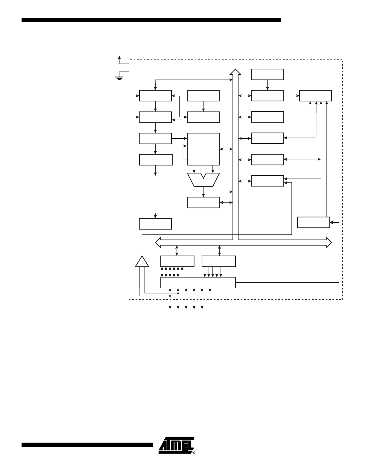
Figure 1. The ATtiny11 Block Diagram
VCC
GND
PROGRAM
COUNTER
STACK
POINTER
8-BIT DATABUS
INTERNAL
OSCILLATOR
WATCHDOG
TIMER
ATtiny11/12
TIMING AND
CONTROL
PROGRAM
FLASH
INSTRUCTION
REGISTER
INSTRUCTION
DECODER
CONTROL
LINES
PROGRAMMING
LOGIC
ANALOG
DATA REGISTER
ARATOR
COMP
+
PORTB
PORTB DRIVERS
HARDWARE
STACK
GENERALPURPOSE
REGISTERS
Z
ALU
STATUS
REGISTER
DATA DIR.
REG. PORTB
MCU CONTROL
REGISTER
MCU STATUS
REGISTER
TIMER/
COUNTER
INTERRUPT
UNIT
OSCILLATORS
1006D–AVR–07/03
PB0-PB5
3

ATtiny12 Block Diagram Figure 2. The ATtiny12 Block Diagram
VCC
GND
PROGRAM
COUNTER
STACK
POINTER
8-BIT DATA BUS
INTERNAL
OSCILLATOR
WATCHDOG
TIMER
INTERNAL
CALIBRATED
OSCILLATOR
TIMING AND
CONTROL
PROGRAM
FLASH
INSTRUCTION
REGISTER
INSTRUCTION
DECODER
CONTROL
LINES
PROGRAMMING
LOGIC
ANALOG
DATA REGISTER
ARATOR
COMP
+
PORTB
PORTB DRIVERS
HARDWARE
STACK
GENERALPURPOSE
REGISTERS
Z
ALU
STATUS
REGISTER
SPI
DATA DIR.
REG. PORTB
MCU CONTROL
REGISTER
MCU STATUS
REGISTER
TIMER/
COUNTER
INTERRUPT
UNIT
EEPROM
OSCILLATORS
PB0-PB5
The ATtiny12 provides the following features: 1K bytes of Flash, 64 bytes EEPROM, up
to six general-purpose I/O lines, 32 general-purpose working registers, an 8-bit
timer/counter, internal and external interrupts, programmable W atchdog Timer w ith
internal oscillator, and two software-selectable power-saving modes. The Idle Mode
stops the CPU while allowing the timer/counters and interrupt system to continue functioning. The Power-d own M ode s aves th e regist er conte nts but freezes the o scillator,
disabling all other chip functions until the next interrupt or hardware reset. The wake-up
or interrupt on pin change features enable the ATtiny12 to be highly responsive to external events, still feat uring the lowest power consumpt ion while i n the power- down modes .
The device is manufactured using Atmel’s high-density nonvolatile memory technology.
By combining an RISC 8-bit CPU with Flash on a monolithic chip, the Atmel ATtiny12 is
a powerful mic rocontro ller that provide s a highly-fl exible and cost -effec tive solution to
many embedded control applications.
4
ATtiny11/12
1006D–AVR–07/03

ATtiny11/12
The ATtiny12 AVR is supported with a full suite of program and system development
tools including: macro assemblers, progra m debugger/s imulators, in-circuit emulators,
and evaluation kits.
Pin Descriptions
VCC Supply voltage pin. GND Ground pin. Port B (PB5..PB0) Port B is a 6-bit I/O port. PB4..0 are I/O pins that can provide internal pull-ups (selected
for each bit). On ATtiny11, PB5 is input onl y. On ATtiny12, PB 5 is input or open-drain
output. The port p ins are t ri-stated w hen a res et con dition be comes a ctive, even if the
clock is not running. The use of pins PB5..3 as input or I/O pins is limited, depending on
reset and clock settings, as shown below.
Table 2. PB5..PB3 Functionality vs. Device Clocking Options
Device Clocking Option PB5 PB4 PB3
External Reset Enabled Used
External Reset Disabled Input
External Crystal - Used Used
(1)
(3)
(4)
/I/O
(2)
-
--
-
External Low-frequency Crystal - Used Used
External Ceramic Resonator - Used Used
External RC Oscillator - I/O
External Clock - I/O Used
Internal RC Oscillator - I/O I/O
Notes: 1. “Used” means the pin is used for reset or clock purposes.
2. “-” means the pin function is unaffected by the option.
3. Input means the pin is a port input pin.
4. On ATtiny11, PB5 is input only. On ATtiny12, PB5 is input or open-drain output.
5. I/O means the pin is a port input/output pin.
(5)
Used
XTAL1 Input to the inverting oscillator amplifier and input to the internal clock operating circuit. XTAL2 Output from the inverting oscillat or amplifier.
RESET
Reset input. An external reset is generated by a low level on the RESET pin. Reset
pulses longer than 50 ns will generate a reset, even if the clock is not running. Shorter
pulses are not guaranteed to generat e a reset.
Clock Options The device has the f ollowing clock source op tions, selectable by Flash fuse bit s as
shown:
Table 3. Device Clocking Options Select
1006D–AVR–07/03
Device Clocking Option ATtiny11 CKSEL2..0 ATtiny12 CKSEL3..0
External Crystal/Ceramic Resonator 111 1111 - 1010
External Low-frequency Crystal 110 1001 - 1000
External RC Oscillator 101 0111 - 0101
5
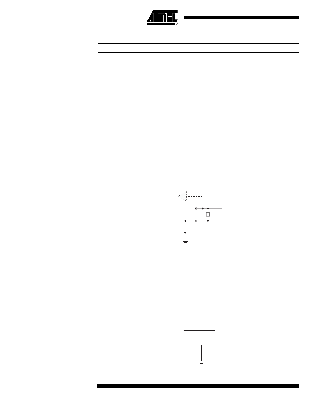
Table 3. Device Clocking Options Select (Continued)
Device Clocking Option ATtiny11 CKSEL2..0 ATtiny12 CKSEL3..0
Internal RC Oscillator 100 0100 - 0010
External Clock 000 0001 - 0000
Reserved Other Options -
Note: “1” means unprogrammed, “0” means programmed.
The various choices for ea ch clocking op tion give different start-u p times as shown in
Table 7 on page 18 and Table 9 on page 20.
Internal RC Oscillator The internal RC oscillator option is an on-chip oscil lat or running at a f ixed frequency of 1
MHz in ATtiny11 and 1.2 MHz in ATtiny12. If selected, the device can operate with no
external components. The device is shipped with this option selected. On ATtiny11, the
Watchdog Oscillator is used as a clock, while ATtiny12 uses a separate calibrated
oscillator.
Crystal Oscillator XTAL1 and XTAL2 are input and o utput , respectively, of an inverting amplifier which can
be configured for use as an on-chip oscillator, as shown in Figure 3. Either a quartz
crystal or a ceramic resonator may be used. Maximum frequency for crystal and resonators is 4 MHz. Minimum voltage for running on a low-frequency crystal is 2.5V.
Figure 3. Oscillator Connections
MAX 1 HC BUFFER
HC
C2
C1
Note: When using the MCU Oscillator as a clock for an external device, an HC buffer should be
connected as indicated in the figure.
XTAL2
XTAL1
GND
External Clock To drive the device from an external clock source, XTAL1 should be driven as shown in
Figure 4.
Figure 4. External Clock Drive Configurati on
PB4 (XTAL2)
EXTERNAL
OSCILLATOR
XTAL1
SIGNAL
GND
6
ATtiny11/12
1006D–AVR–07/03

ATtiny11/12
External RC Oscillator For timing insensitive applications, the external RC configuration shown in Figure 5 can
be used. For details on how to choose R and C, see Table 29 on page 59. The external
RC oscillator is sensitive to noise from neigh boring pins, and to avoid proble ms, PB5
(RESET
put pin.
Figure 5. External RC Configuration
) should be used as an output or reset pin, and PB4 should be used as an out-
VCC
R
C
PB4 (XTAL2)
XTAL1
GND
1006D–AVR–07/03
7

Architectural Overview
The fast-access register file concept contains 32 x 8-bit general-purpose working registers with a single-clock-cycle access time. This means that du ring one sing le clock
cycle, one ALU (Arithmetic Logic Unit) operation is executed. Two operands are output
from the register file, the operation is executed, and the result is stored back in the register file – in one clock cycle.
Two of the 32 registers can be used as a 16-bit pointer for indirect memory access. This
pointer is called the Z-pointer, and can address the register file and the Flash program
memory.
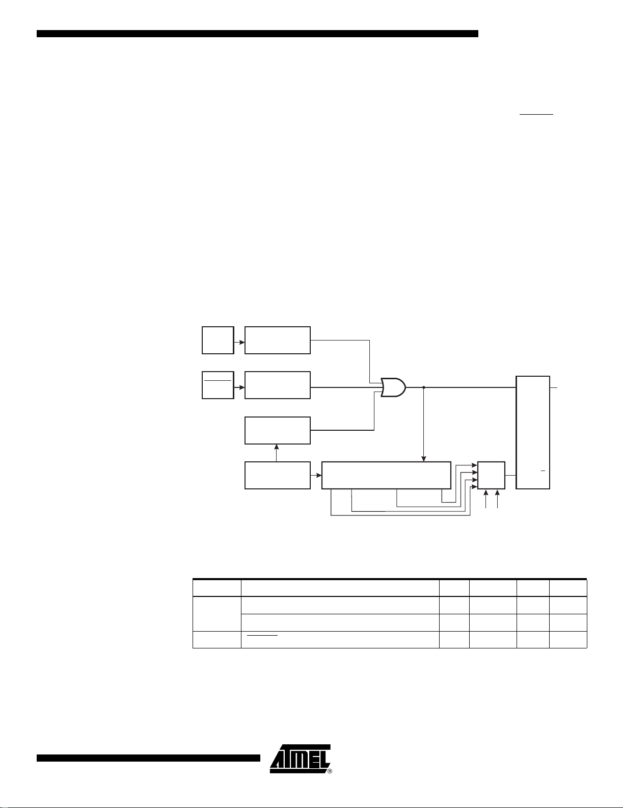
The ALU supp orts arithm etic and log ic fun ctions betwe en reg isters or b etween a co nstant and a register. Sin gle-register operati ons are also e xecuted in the A LU. Figure 2
shows the AT tiny1 1/12 AVR RISC mic rocont roller arc hitectu re. The A VR use s a Harvard architecture concept with separate memori es and buses for progra m and data
memories. The program memory is accessed with a two-stage pipelining. While one
instruction is being executed, the next instruction is pre-fetched from the program memory. This concept enables instructions to be executed in every clock cycle. The program
memory is reprogrammable Flash memory.
With the relative jump and relative call instructions, the whole 512 address space is
directly accessed. All A VR instructio ns have a single 16-bit word f ormat, mea ning that
every program memory address contains a single 16-bit instruction .
During interrupts and subroutine calls, the return address program counter (PC) is
stored on the stack . Th e stack i s a 3 -level-deep hardware stack de dicated for subroutines and interrupts.
The I/O memory space con tains 64 addresses f or CPU peri pheral functions as cont rol
registers, timer/counters, and other I/O functions. The memory spaces i n the AVR architecture are all linear and regular memory maps.
8
ATtiny11/12
1006D–AVR–07/03

Figure 6. The ATtiny11/12 AVR RISC Architecture
8-bit Data Bus
ATtiny11/12
512 x 16
Program
Flash
Instruction
Register
Instruction
Decoder
Control Lines
Program
Counter
Direct Addressing
Status
and Test
32 x 8
General-
purpose
Registers
ALU
64 x 8 EEPROM
(ATtiny12 only)
Control
Registers
Interrupt
Unit
SPI Unit
(ATtiny12 only)
8-bit
Timer/Counter
Watchdog
Timer
Analog
Comparator
6
I/O Lines
A flexible inte rrupt modu le has its con trol regist ers in the I/O space with an additio nal
global interrupt enable bit in the status register. All the different interrupts have a separate interrupt vector in the interrupt vector tab le at the beginning of the
program memory. The different interrupts have priority in accordance with their interrupt
vector position. The lower the interrupt vector address, the higher the priority.
General-purpose Register File
1006D–AVR–07/03
Figure 7 shows the structure of the 32 general-purpose registers in the CPU.
Figure 7. AVR CPU General-purpose Working Registers
70
R0
R1
R2
General- …
purpose …
Working R28
Registers R29
R30 (Z-register low byte)
R31 (Z-r egister high byte)
All the register operating instructions in the instruction set have direct- and single-cycle
access to a ll regist ers. The only excepti on is the five c onstan t arithm etic an d logic
instructions SBCI, SUBI, CPI, ANDI, and ORI between a constant and a register and the
LDI instruction for load-immediate constant data. These instructions apply t o the second
half of the registe rs in the register f ile – R16..R 31. The genera l SBC, SU B, CP, AND,
9

OR and all o ther op eration s bet ween two re gisters or on a si ngle reg ister apply to the
entire register file.
Registers 30 and 31 form a 16-bit pointer (the Z-pointer) which is used for indirect Flash
memory and register fil e access. When the register file is accessed, t he contents of R31
are discarded by the CPU.
ALU – Arithmetic Logic Unit
The high-performance AVR ALU operat es in d irect con nection with all the 32 gene ralpurpose working registers. Wit hin a sing le clock cycle , ALU op erations be tween registers in the register file are executed. The ALU operations are divided into three main
categories – arithmetic, logic and bit-functions. Some microcontrollers in the AVR product family feature a hardware multiplier in the arithmetic part of the ALU.
Flash Program Memory The ATtiny11/12 contain s 1K bytes on-chip Flash me mory for program storag e. Since
all instructions are single 16-bit words, the F lash is organized as 5 12 x 16 words. T he
Flash memory has an endurance of at least 1000 write/er ase cycles.
The ATtiny11/12 Program Counter is 9 bits wide, thus addressing the 512 words Flash
program memory.
See page 46 for a detailed description on Flash memory programming.
Program and Data Addressing Modes
Register Direct, Single Register Rd
The ATtiny11/12 AVR RISC Microcontroller supports powerful and efficient addressing
modes. This se ction describes the different addressin g modes supported i n the
ATtiny11/12. In the figures, OP means the ope ration code part of the instruction word.
To simplify, not all figure s show the exact location of the addressing bits.
Figure 8. Direct Single-register Addressing
10
The operand is contained in regist er d (Rd).
ATtiny11/12
1006D–AVR–07/03

Register Indirect Figure 9. Indirect Register Addressing
ATtiny11/12
REGISTER FILE
0
The register accessed is the one pointed to by th e Z-register (R31, R30).
Register Direct, Two Registers
Figure 10. Direct Register Addressing, Two Registers
Rd and Rr
Operands are contained in register r (Rr) and d (Rd). The result is store d in regi ster d
(Rd).
I/O Direct Figure 11. I/O Direct Addressing
Z-register
30
31
1006D–AVR–07/03
Operand addres s is con taine d in 6 bit s of the instruc tion wor d. n is the desti natio n or
source register address.
11

Relative Program Addr essing, RJMP and RCALL
Figure 12. Relative Program Memor y Addressing
+1
Program execution continues at address PC + k + 1. The relative address k is -2048 to
2047.
Constant Addressing Using the LPM Instruction
Subroutine and Interrupt Hardware Stack
Figure 13. Code Memory Constant Addressing
PROGRAM MEMORY
15 1 0
Z-REGISTER
$000
$1FF
Constant byte address is specified by the Z-register contents. The 15 MSBs select word
address (0 - 511) , the LSB sel ects low byte i f cleare d (LSB = 0) or hi gh byte if set
(LSB = 1).
The ATtiny11/12 uses a 3-level -deep hardwar e st ack for subr outin es and inter rupts. The
hardware stack is 9 bits wide and stores the program counter (PC) return address while
subroutines and inter rupt s are executed.
RCALL instructi ons an d int errupts pu sh th e PC return a ddress o nto stack l evel 0, a nd
the data in the other stack levels 1-2 are pushed one level deeper in the stack. When a
RET or RETI instruction is executed the returning PC is fetched from stack level 0, and
the data in the other stack level s 1-2 are popped one level in the stack.
12
If more than three subsequent subroutine calls or interrupts are executed, the first values written to the stack are overwritten. Pushing four return addresses A1, A2, A3, and
A4, followed by four subroutine or interrupt returns, will pop A4, A3, A2, and once more
A2 from the hardware stack.
ATtiny11/12
1006D–AVR–07/03

ATtiny11/12
EEPROM Data Memory The ATtiny12 contains 64 bytes of data EEPROM memory. It is organized as a separate
data space, in which single bytes can be read and written. The EEPROM has an endurance of at least 100,000 write/erase cycles. The access between the EEPROM and the
CPU is described on page 38, specifying the EEPROM Address Register, the EEPROM
Data Register, and the EEPROM Control Register.
For SPI data downloading, see “Memory Programming” on page 46 for a detailed
description.
Memory Access and Instruction Execution Timing
This section describes the general access timing concepts for instruction execution and
internal memory access.
The AVR CPU is driven by the System Clock Ø, directly generated from the external
clock crystal for the chip. No internal clock division is used.
Figure 14 shows the parallel instruction fet ches and instruction e xecutions enab led by
the Harvard architecture and the fast-access register file concept. This is the basi c pipelining concept to obtain up to 1 MIPS per MHz with the corresponding unique results for
functions per cost, functions per clocks, and functions per po wer-unit.
Figure 14. The Parallel Instruc ti on Fetches and Instruction Executions
T1 T2 T3 T4
System Clock Ø
1st Instruction Fetch
1st Instruction Execute
2nd Instruction Fetch
2nd Instruction Execute
3rd Instruction Fetch
3rd Instruction Execute
4th Instruction Fetch
Figure 15 shows the internal timing concept for the register file. In a single clock cycle,
an ALU operation using two register operands is executed and the result is stored back
to the destination regis ter.
1006D–AVR–07/03
Figure 15. Single-cycle ALU Operation
T1 T2 T3 T4
System Clock Ø
Total Execution Time
Register Operands Fetch
ALU Operation Execute
Result Write Back
13

I/O Memory The I/O space definition of the ATtiny11/12 is shown in the following table:
Table 4. ATtiny11/12 I/O Space
Address Hex Name Device Function
$3F SREG ATtiny11/12 Status Register
$3B GIMSK ATtiny11/12 General Interrupt Mask Register
$3A GIFR ATtiny11/12 General Interrupt Flag Register
$39 TIMSK ATtiny11/12 Timer/Counter Interrupt Mask Register
$38 TIFR ATtiny11/12 Timer/Counter Interrupt Flag Register
$35 M CUCR ATtiny11/12 MCU Control Register
$34 MCUSR ATtiny11/12 MCU Status Register
$33 T CCR0 ATtiny11/12 Timer/Counter0 Control Register
$32 TCNT0 ATtiny11/12 Timer/Counter0 (8-bit)
$31 OSCCAL ATtiny12 Oscillator Calibration Register
$21 WDTCR ATtiny11/12 Watchdog Timer Control Register
$1E EEAR ATtiny12 EEPROM Address Register
$1D EEDR ATtiny12 EEPROM Data Register
$1C EECR ATtiny12 EEPROM Control Register
$18 PORTB ATtiny11/12 Data Register, Port B
$17 DDRB ATtiny11/12 Data Direction Register, Port B
$16 PINB ATtiny11/12 Input Pins, Port B
$08 ACSR ATtiny11/12 Analog Comparator Control and Status Register
Note: Reserved and unused locations are not shown in the table.
All the different ATtiny11/12 I/O and peripherals are placed in the I/O space. The different I/O locations are acce ssed by the I N and OUT instruc tions t ransfer ring data bet ween
the 32 general-purpose working registers and the I/O space. I/O registers within the
address range $00 - $1F are directly bit-accessible using the SBI and CBI instructions.
In these registers, the value of single bits can be checked by using the SBIS and SBIC
instructions. Refer to the Instruction Set Summary for more details.
For compatibility wit h future devices, rese rved bits should be writte n to zero if accessed.
Reserved I/O memory addressed should never be written.
The different I/O and peripherals control regi sters are explained in t he following
sections.
Status Register – SREG The AVR status register (SREG) at I/O space location $3F is defi ned as:
Bit 76543210
$3F ITHSVNZCSREG
Read/Write R/W R/W R/W R/W R/W R/W R/W R/W
Initial Value00000000
14
• Bit 7 - I: Globa l Int e rrupt Ena ble
The global interru pt enable bit must be set (one) for the interru pts to be ena bled. The
individual interrupt enable control is then performed in separate control registers. If the
ATtiny11/12
1006D–AVR–07/03

ATtiny11/12
global interrupt enab le regi ster i s cleared (zero), none of the i nterr upt s are enable d independent of the individual interrupt enable settings. The I-bit is cleared by hardware after
an interrupt has occurre d, and is set by the RETI instruc tion to enable subs equent
interrupts.
• Bit 6 - T: Bit Copy Storage
The bit copy instructio ns BLD (B it LoaD) and BST (Bit STore) use the T-bit as source
and destination for t he oper ated bi t. A bit from a register i n the r egister fil e can be copi ed
into T by the BST instruction, and a bit i n T can be copied into a b it in a reg ister in the
register file by the BLD instruction.
• Bit 5 - H: Half Carry Flag
The half carry flag H indicates a half-carry in some arithmetic operations. See the
Instruction Set descri p ti on for detailed information.
• Bit 4 - S: Sign Bit, S = N ⊕ V
The S-bit is always an exclusive or between the negative flag N and the two’s complement overflow flag V. See the Instruction Set description for detailed information.
• Bit 3 - V: Two’s Complement Overflow Flag
Reset and Interrupt Handling
The two’s complem ent overflow flag V sup ports tw o’s co mplemen t arit hmetic. See t he
Instruction Set descri p ti on for detailed information.
• Bit 2 - N: Negative Flag
The negative flag N indicates a negative result from an arithmetical or logical operation.
See the Instruction Set description for detailed information.
• Bit 1 - Z: Zero Flag
The zero flag Z indicates a zero result from an arithmetical or logical operation. See the
Instruction Set descri p ti on for detailed information.
• Bit 0 - C: Carry Flag
The carry flag C ind icates a carry in an arithmet ical or logical operat ion. See the Instruction Set description for detailed information.
Note that the status register is not automatically stored when entering an interrupt routine and restored when returning from an interrupt routine. This must be handled by
software.
The ATtiny11 provi des four differe nt interrupt sou rces and the AT tiny12 prov ides five.
These interrupts and the separate reset vector each have a separate program vector in
the program memory space. All the interrupts are assigned individual enable bits which
must be set (one) together with the I-bit in the status register in order to enable the
interrupt.
1006D–AVR–07/03
The lowest addresse s in the program me mory space are au tomaticall y defined as the
Reset and Interrupt vectors. The complete list of vectors is shown in Table 5. The list
also determines the priority levels of the different interrupts. The lower the address, the
higher the priority level. RESET has the highest priority, and next is INT0 – the External
Interrupt Request 0, etc.
15

Table 5. Reset and Interrupt Vectors
Vector No. Device Program Address Source Inte r rupt Definition
External Pin, Power-on
1 ATtiny11 $000 RESET
1 ATtiny12 $000 RESET
Reset and Watchdog
Reset
External Pin, Power-on
Reset, Brown-out Reset
and Watchdog Reset
2 ATtiny11/12 $001 INT0
External Interrupt
Request 0
3 ATtiny11/12 $002 I/O Pins Pin Change Interrupt
4 ATtiny11/12 $003 TIMER0, OVF0
Timer/Counter0
Overflow
5 ATtiny11 $004 ANA_COMP Analog Comp arator
5 ATtiny12 $004 EE_RDY EEPROM Ready
6 ATtiny12 $005 ANA_COMP Analog Comp arator
The most typical and general program setup for the reset and i nterru pt vector address es
for the ATtiny11 are:
Address Labels Code Comments
$000 rjmp RESET ; Reset handler
$001 rjmp EXT_INT0 ; IRQ0 handler
$002 rjmp PIN_CHANGE ; Pin change handler
$003 rjmp TIM0_OVF ; Timer0 overflow handler
$004 rjmp ANA_COMP ; Analog Comparat or handler
;
$005 MAIN: <instr> xxx ; Main program start
… … … …
The most typical and general program setup for the reset and i nterru pt vector address es
for the ATtiny12 are:
Address Labels Code Comments
$000 rjmp RESET ; Reset handler
$001 rjmp EXT_INT0 ; IRQ0 handler
$002 rjmp PIN_CHANGE ; Pin change handler
$003 rjmp TIM0_OVF ; Timer0 overflow handler
$004 rjmp EE_RDY ; EEPROM Ready handler
$005 rjmp ANA_COMP ; Analog Comparat or handler
;
$006 MAIN: <instr> xxx ; Main program start
… … … …
16
ATtiny11/12
1006D–AVR–07/03
Reset Sources The ATtiny11/12 provides three or four sources of reset:
• Power-on Reset. The MCU is reset when the supply voltage is below the power-on
reset threshold (V
POT
).
• External Reset. The MCU is reset when a low level is present on the RESET
more than 50 ns.
• Watchdog Reset. The MCU is reset when the Watchdog timer period expires and
the Watchdog is enabled.
• Brown-out Reset. The MCU is reset when the supply voltage V
certain voltage (ATtiny12 only).
During reset, all I/O registers are then set to their initial values, and the program starts
execution from address $000. The instruction placed in address $000 mu st be an RJMP
– relative jump – instruction to the reset handling routine. If the program never enables
an interrupt source, the interrupt vectors are not used, and regular program code can be
placed at these locations. The circuit diagram in Figure 16 shows the reset logic for the
ATtiny11. Figure 17 shows the reset logic for the ATt iny12. Table 6 defines the electrical
parameters of the reset circui try fo r ATtiny1 1. Table 8 shows t he para meters of t he reset
circuitry for ATtiny12.
Figure 16. Reset Logic for the ATtiny11
VCC
Power-on Reset
Circuit
POR
ATtiny11/12
pin for
falls belo w a
CC
RESET
Reset Circuit
Watchdog
Timer
On-chip
RC Oscillator
COUNTER RESET
20-stage Ripple Counter
Q3 Q19
Q9
Q13
CKSEL
FSTRT
QS
Q
R
Table 6. Reset Characteristics for the ATtiny11
Symbol Parameter Min Typ Max Units
Power-on Reset Threshold Voltage (rising) 1.0 1.4 1.8 V
(1)
V
POT
V
RST
Note: 1. The Power-on Reset will not work unless the supply voltage has been below V
Power-on Reset Threshold Voltage (falling) 0.4 0.6 0.8 V
RESET Pin Threshold Voltage 0.6 V
CC
(falling).
V
INTERNAL
RESET
POT
1006D–AVR–07/03
17

Power-on Reset for the ATtiny11
A Power-on Reset (POR) circuit ensures that the device is reset from power-on. As
shown in Figure 16, an in ternal timer is clocked from the watchdog timer. This t imer prevents the MCU from starting a certain period after V
Threshold Voltage – V
period – t
. The FSTRT fuse bit in the Flash can be programmed to give a shorter
TOUT
. See Figure 18. The total reset period is the Delay Tim e-out
POT
has reached the Power-on
CC
start-up time.The start-up times for the different clock options are shown in the following
table. The Watchdog Oscillator is used for timing the start-up time, and this oscillator is
voltage dependent as shown in the section “A Ttiny11 Typical Charact eristics” on page
60.
Table 7. Start-up Times for the ATtiny11 (V
Selected Clock Opti on
External Crystal 67 ms 4.2 ms
External Ceramic Resonator 67 ms 4.2 ms
External Low-frequency Crystal 4.2 s 4.2 s
External RC Oscillator 4.2 ms 67 µs
Internal RC Oscillator 4.2 ms 67 µs
External Clock 4.2 ms
FSTRT Unprogrammed FSTRT Programmed
If the built-in start-up delay is sufficient, RESET
an external pull-up resistor. By holding the RESET
= 2.7V)
CC
Start-up Time t
TOUT
5 clocks from reset,
2 clocks from power-down
can be connected to VCC directly or via
pin low for a period after VCC has
been applied, the Power-on Reset period can be extended. Refer to Figure 19 for a timing example on this.
18
ATtiny11/12
1006D–AVR–07/03
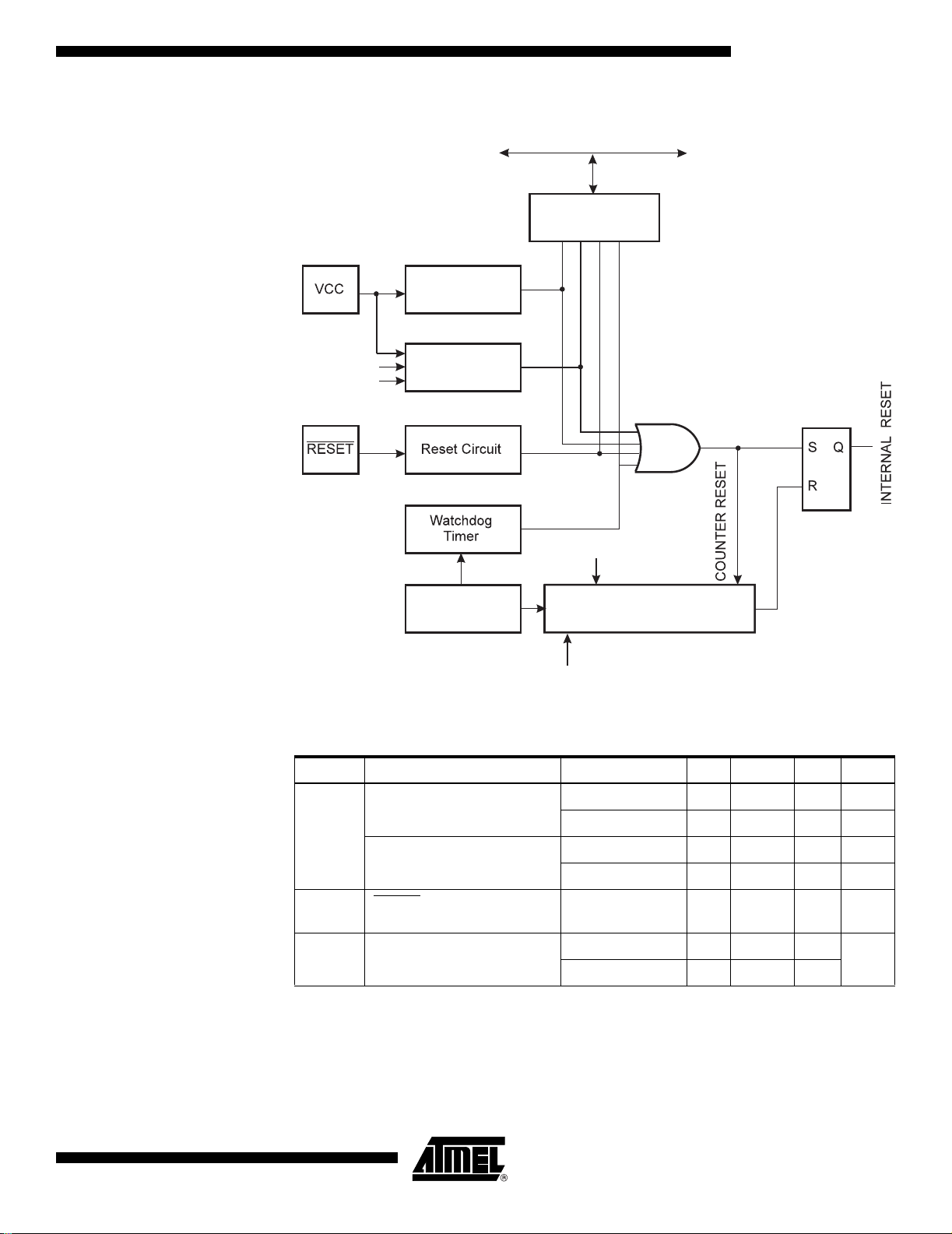
Figure 17. Reset Logic for the ATtiny12
DATA BUS
MCU Status
Register (MCUSR)
Power-on Reset
Circuit
PORF
BORF
EXTRF
ATtiny11/12
WDRF
BODEN
BODLEVEL
Brown-out
Reset Circuit
CKSEL[3:0]
On-chip
RC Oscillator
Delay Counters
Full
CK
Table 8. Reset Characteristics for the ATtiny12
Symbol Parameter Condition Min Typ Max Units
Power-on Reset Threshold
V ol tage (risin g)
(1)
V
POT
Power-on Reset Threshold
V oltage (falling)
BOD disabled 1.0 1.4 1.8 V
BOD enabled 0.6 1.2 1.8 V
BOD disabled 0.4 0.6 0.8 V
BOD enabled 0.6 1.2 1.8 V
1006D–AVR–07/03
V
V
RST
BOT
RESET Pin Threshold
Voltage
Brown-out Re set Threshold
Voltage
0.6V
CC
(BODLEVEL = 1) 1.5 1.8 1.9
(BODLEVEL = 0) 2.3 2.7 2.8
V
V
Note: 1. The Power-on Reset will not work unless the supply voltage has been below V
(falling).
POT
19

Table 9. ATtiny12 Clock Options and Start-up Times
Start- up Time,
VCC = 1.8V,
BODLEVEL
CKSEL3..0 Clock Source
1111 Ext. Crystal/Ceramic Resonator
1110 Ext. Crystal/Ceramic Resonator
1101 Ext. Crystal/Ceramic Resonator
1100 Ext. Crystal/Ceramic Resonator 16K CK 16K CK
1011 Ext. Crystal/Ceramic Resonator 3.6 ms + 16K CK 4.2 ms + 16K CK
1010 Ext. Crystal/Ceramic Resonator 57 ms + 16K CK 67 ms + 16K CK
1001 Ext. Low-frequency Crystal 57 ms + 1K CK 67 ms + 1K CK
1000 Ext. Low-frequency Crystal 57 ms + 32K CK 67 ms + 32K CK
0111 Ext. RC Oscillator 6 CK 6 CK
0110 Ext. RC Oscillator 3.6 ms + 6 CK 4.2 ms + 6 CK
0101 Ext. RC Oscillator 57 ms + 6 CK 67 ms + 6 CK
0100 Int. RC Oscillator 6 CK 6 CK
0011 Int. RC Oscillator 3.6 ms + 6 CK 4.2 ms + 6 CK
0010 Int. RC Oscillator 57 ms + 6 CK 67 ms + 6 CK
0001 Ext. Clock 6 CK 6 CK
Unprogrammed
(1)
1K CK 1K CK
(1)
3.6 ms + 1K CK 4.2 ms + 1K CK
(1)
57 ms 1K CK 67 ms + 1K CK
Start-up Time,
VCC = 2.7V,
BODLEVEL
Programmed
0000 Ext. Clock 3.6 ms + 6 CK 4.2 ms + 6 CK
Note: 1. Due to the limited number of clock cycles in the start-up period, it is recommended
that Ceramic Resonator be used.
This table shows the start-up times from reset. From sleep, only the clock counting part
of the start-up time is used. The Watchdog oscillator is used for timing the real-time part
of the start-up time. The number of WDT oscillator cycles used for each time-out is
shown in Table 10.
Table 10. Number of Watchdog Oscillator Cycl es
BODLEVEL Time-out Number of Cycles
Unprogrammed 3.6 ms (at Vcc = 1.8V) 256
Unprogrammed 57 ms (at Vcc = 1.8V) 4K
Programmed 4.2 ms (at Vcc = 2.7V) 1 K
Programmed 67 ms (at Vcc = 2.7V) 16K
The frequency of the watchdog oscillator is voltage dependent as shown in the section
“ATtiny11 Typical Characteristics” on page 60.
Note that the BODL EVEL fuse can be used to select start-up times even if the Brownout Detection is disabled (by leaving the BODEN fuse unprogrammed).
The device is shipped with CKSEL3..0 = 0010.
20
ATtiny11/12
1006D–AVR–07/03

ATtiny11/12
Power-on Reset for the ATtiny12
A Power-on Reset (POR) pulse is generated by an on-chip detection circuit. The detection level is nominally 1.4V. The POR is activated whenever V
is below the detection
CC
level. The POR circuit can be used to trigger the start-up reset, as well as detect a failure in supply voltage.
The Power-on Rese t (POR) circuit en sures that th e device is reset from pow er-on.
Reaching the Power-on Reset threshold voltage i nvokes a delay cou nter, which determines the delay for which the device is kept in Reset after V
rise. The time-out period
CC
of the delay counter can be defined by the user through the CKSEL fuses. The different
selections for the del ay period are pre sented i n Table 9 . The Reset signa l is act ivated
again, without any delay, when the V
If the built-in start-up delay is sufficient, RESET
an external pull-up resistor. See Figure 18. B y holding t he RESET
after V
has been applied, the Power-on Reset period can be extended. Refer to Fig-
CC
decreases below detection level.
CC
can be connected to VCC directly or via
pin low for a period
ure 19 for a timing example on this.
t
TOUT
Tied to VCC.
Figure 18. MCU Start-up, RESET
V
V
CC
RESET
TIME-OUT
POT
V
RST
INTERNAL
RESET
Figure 19. MCU Start-up, RESET
V
V
RESET
TIME-OUT
INTERNAL
RESET
CC
POT
Extended Externally
V
RST
t
TOUT
External Reset An external reset is generated by a low level on the RESET
than 50 ns will generate a reset, even if the clock is not running. Shorter pulses are not
guaranteed to generate a reset. When the applied signal reaches the Rese t Threshold
Voltage – V
period (t
– on its positive edge, the delay timer starts the MCU after the Time-out
RST
) has expired.
TOUT
pin. Reset pulses longer
1006D–AVR–07/03
21

Figure 20. External Reset during Op eration
V
CC
Brown-out Detection (ATtiny12)
RESET
TIME-OUT
INTERNAL
RESET
ATtiny12 has an on-chip brown-out detection (BOD) circuit for monitoring the V
V
RST
t
TOUT
level
CC
during the operation. The BOD circuit can be enabled/disabled by the fuse BODEN.
When BODEN is enabled (BODEN programmed), and V
level, the brown-out reset is immediately activated. When V
decreases below the trigger
CC
increases above the trig-
CC
ger level, the b rown-out reset is dea ctivated after a delay. T he delay i s defined by the
user in the sa me w ay a s t he de lay of P OR s ignal , in Tab le 5. The trig ger l evel for the
BOD can be selected by the fuse BODLEVEL to be 1.8V (BODLEVEL unprogrammed),
or 2.7V (BODLEVEL programmed). The trigger level has a hysteresis of 50 mV to
ensure spike-free bro wn -out detection.
The BOD circuit will only detect a drop in V
if the voltage stays below the trigger level
CC
for longer than 7 µs for trigger level 2.7V, 24 µs for trigger level 1.8V (typical values).
Figure 21. Brown-out Reset during Operation (ATtiny12)
V
CC
RESET
TIME-OUT
INTERNAL
RESET
Note: The hysteresis on V
BOT
: V
V
BOT-
BOT +
= V
+ 25 mV, V
BOT
BOT-
= V
V
BOT
BOT+
t
TOUT
- 25 mV.
22
ATtiny11/12
1006D–AVR–07/03

ATtiny11/12
Watchdog Reset When the Watchdog times out, it will generate a short reset pulse of 1 CK cycle dura-
tion. On the falling edge of this puls e, the delay timer start s countin g the Time-out period
). Refer to page 36 for details on operation of the Watc hdog.
(t
TOUT
Figure 22. Watchdog Reset during Operation
V
CC
CK
MCU Status Register – MCUSR of the ATtiny11
The MCU Status Register provides information on which reset source caused an M CU
reset.
Bit 76543210
$34 ------EXTRFPORFMCUSR
Read/WriteRRRRRRR/WR/W
Initial Value000000See bit description
• Bit 7..2 - Res: Reserved Bits
These bits are reserved bit s in t he ATtiny11 and always read as zero.
• Bit 1 - EXTRF: EXT ernal Reset Flag
After a power-on reset, this bit is undefined (X). It will be set by an external reset. A
watchdog reset will leave this bit unchan ged.
• Bit 0 - PORF: Power-on Reset Flag
This bit is set by a power-on reset. A watchdog reset or an external reset will leave this
bit unchanged.
To summarize, the follow ing table show s the value o f these two bits a fter the three
modes of reset.
Table 11. PORF and EXTRF Values afte r Re set
Reset Source EXTRF PORF
1006D–AVR–07/03
Power-on Undefined 1
External Reset 1 Unchanged
Watchdog Reset Unchanged Unchanged
To identify a reset condition, the user software should clear both the PORF and EXTRF
bits as early as possible in the program. Checking the PORF and EXTRF values is done
23

before the bits are cleared. If the bit is cleared before an external or watchdog reset
occurs, the source of reset can be found by using the following truth table:
Table 12. Reset Source Identification
EXTRF PORF Reset Source
0 0 Watchdog Reset
1 0 External Reset
0 1 Power-on Reset
1 1 Power-on Reset
MCU Status Register – MCUSR for the ATtiny12
The MCU Status Register provides information on which reset source caused an M CU
reset.
Bit 76543210
$34 ----WDRFBORFEXTRFPORFMCUSR
Read/Write R R R R R/W R/W R/W R/W
Initial Valu e 0 0 0 0 See Bit Descri p tion
• Bit 7..4 - Res: Reserved Bits
These bits are reserved bit s in t he ATtiny12 and always read as zero.
• Bit 3 - WDRF: Watchdog Reset Flag
This bit is set if a watchdog reset occurs. The bit is reset by a power-on reset, or by writing a logic zero to the flag.
• Bit 2 - BORF: Brown-out Reset Flag
This bit is set if a brown-out reset occurs . The bit is reset by a power-on reset , or by writ ing a logic zero to the flag.
• Bit 1 - EXTRF: EXT ernal Reset Flag
This bit is set if an external reset occurs. The bit is reset by a power-on reset, or by writing a logic zero to the flag.
ATtiny12 Internal Vo ltage Reference
Voltage Reference Enable Signals and Start-up Time
24
ATtiny11/12
• Bit 0 - PORF: Power-on Reset Flag
This bit is set if a pow er-on reset occu rs. The bit is reset b y writing a logic zero to the
flag.
To use the reset flags to identify a reset condition, the user should read and then reset
the MCUSR as early as possib le i n the program. If the re gister is cleared before another
reset occurs, the source of the reset can be found by examining the reset flags.
ATtiny12 fea tures an intern al voltag e referenc e with a n ominal vo ltage of 1 .22V. T his
reference is used for Brown-out Detection, and it can be used as an input to the Analog
Comparator.
The voltage reference has a start-up time that may influence the way it should be used.
The maximum start-up time is 10µs. To save power, the reference is not always turned
on. The reference is on during the follo wing situations:
1006D–AVR–07/03

ATtiny11/12
1. When BOD is enabled (by programming the BODEN fuse)
2. When the bandgap refere nce is conn ected to the Analog Comp arato r (by setting
the AINBG bit in ACSR)
Thus, when BOD is not enabled, after setti ng the AINBG bit, the user must always allow
the reference to start up before the output from the Analog Comparator is used. The
bandgap reference uses approximately 10 µA, and to reduce power consumption in
Power-down mode, the user can turn off the reference when entering this mode.
Interrupt Handling The ATtiny11/12 has two 8-bit Interrupt Mask control registers; GIMSK – General Inter-
rupt Mask register and TIMSK – Timer/Counter Interrupt Mask register.
When an interrupt occ urs, the Global Interrupt Enable I-bit is cleared (zero) and all inter-
rupts are disabled. The user software can set (one) the I-bit to enable nested interrupts.
The I-bit is set (one) when a Return from Interrupt instruction – RETI – is executed.
When the Program Counter is vectored to the actual interrupt vector in order to execute
the interrupt handling rou ti ne, hardwar e clears the corre sponding f lag that generated t he
interrupt. Some of t he inter rupt f lags can also be cl eared by wri ting a logic o ne to the flag
bit position(s) to be cl eared.
If an interrupt con dition oc curs when the corres ponding i nterrupt ena ble bit is cleared
(zero), the interrupt flag will be set and remembered until the interrupt is enabled, or the
flag is cleared by software.
If one or more interrupt conditions occur when the global interrupt enable bit is cleared
(zero), the corresponding interrupt flag(s) will be set and remembered until the global
interrupt enable bit is set (one), and will be executed by order of pr iority.
Note that external level interrupt does not have a flag, and will only be remembered for
as long as the interrupt condit ion is active.
Note that the status register is not automatically stored when entering an interrupt routine and restored when returning from an interrupt routine. This must be handled by
software.
Interrupt Response Time The interrupt execution response for all the enabled AVR interrupts is 4 clock cycles
minimum. After the 4 clock cycles, the program vector address for the actual interrupt
handling routine is executed. D uring this 4-clock-cycle period, the Prog ram Counter (9
bits) is pushed onto the Stack. The vec tor is normall y a relative j ump to the interru pt rou tine, and this jump takes 2 clock cycles. If an interrupt occurs during execution of a
multi-cycle instruction, this instruction is completed before the interrupt is served. In
ATtiny12, if an interrupt occurs when the MCU is in Sleep mode, the interrupt response
time is increased by 4 clock cycles.
A return from an interrupt handling routine takes 4 clock cycles. During these 4 clock
cycles, the Program Counter (9 bits) is popped back from the Stack, and the I-flag in
SREG is set. When AVR exits from an interrupt, it will always ret urn to the main program
and execute one more instruction bef ore any pending interrupt is served.
General Interrupt Mask Register – GIMSK
Bit 7 6 5 4 3 2 1 0
$3B - INT0 PCIE - - - - - GIMSK
Read/Write R R/W R/W R R R R R
Initial Valu e 0 0 0 0 0 0 0 0
1006D–AVR–07/03
25

General Interrupt Flag Register – GIFR
• Bit 7 - Res: Reserved Bit
This bit is a reserved bit in the ATtiny11/12 and always reads as zero.
• Bit 6 - INT0: E x te r n al In te r ru p t Request 0 E n a ble
When the INT0 bit is set (one) and the I-bit in the Status Register (SREG) is set (one),
the external pin interrupt is enabled. The Interrupt Se nse Control0 bi ts 1/0 (ISC01 and
ISC00) in the MCU general Control Register (MCU CR) define whether the ext ernal
interrupt is activa ted on risin g or fallin g edge, on pin chang e, or low le vel of the INT0 pin .
Activity on the pin will ca use an inter rupt re quest even i f INT0 is co nfigur ed as an output .
The corresponding interrupt of External In terrupt Request 0 is executed from progra m
memory address $001. See also “External Interrupts.”
• Bit 5 - PCIE: Pi n Ch a n g e In te r ru p t Enable
When the PCIE bit is set (one) and the I-bit in the Status Register (SREG) is set (one),
the interrupt on pin change is enabled. Any change on any input or I/O pin will cause an
interrupt. The corresponding interrupt of Pin Change Interrupt Request is executed from
program memory address $002. See also “Pin Change Interrupt.”
• Bits 4..0 - Res: Reserved Bits
These bits are reserved bits in the ATtiny11/12 and always read as zero.
Bit 7 6 5 4 3 2 1 0
$3A - INTF0 PCIF - - - - - GIFR
Read/Write R R/W R/W R R R R R
Initial Valu e 0 0 0 0 0 0 0 0
Timer/Counter Interrupt Mask Register – TIMSK
• Bit 7 - Res: Reserved Bit
This bit is a reserved bit in the ATtiny11/12 and always reads as zero.
• Bit 6 - INTF0 : E x te rnal Interrupt Flag 0
When an edge on the INT0 pin triggers an interrupt request, the corresponding interrupt
flag, INTF0 becomes set (one). If the I-bit in SREG and th e corresponding interrupt
enable bit, INT0 bit in G IMSK, are set (on e), the MCU will jum p to the interrupt ve ctor.
The flag is cleared when the interrupt routine is executed. Alternatively, the flag can be
cleared by writing a logical one to it. The flag is always cleared when INT0 is configur ed
as level inte r ru p t.
• Bit 5 - PCIF: Pin Change Interrupt Flag
When an event on any input or I/O pin triggers an interrupt request, PCIF becomes set
(one). If the I-bit in SREG and the PCIE bit in GIMSK are set (one), the MCU will jump to
the interrupt vector at address $002. The flag is cleared when the interrupt routine is
executed. Alternatively, the flag can be cleared by writing a logical one to it.
• Bits 4..0 - Res: Reserved Bits
These bits are reserved bits in the ATtiny11/12 and always read as zero.
Bit 7 6 5 4 3 2 1 0
26
ATtiny11/12
1006D–AVR–07/03

Timer/Counter Interrupt Flag Register – TIFR
ATtiny11/12
$39 - - - - - - TOIE0 - TIMSK
Read/Write R R R R R R R/W R
Initial Valu e 0 0 0 0 0 0 0 0
• Bit 7..2 - Res: Reserved Bits
These bits are reserved bits in the ATtiny11/12 and always read as zero.
• Bit 1 - TOIE0: Timer/Counter0 Overflow Interrupt Enable
When the TOIE0 bit is set (one) and the I-bit in the Status Register is set (one), the
Timer/Counter0 Overflow interrupt is enabled. The corresponding interrupt (at vector
$003) is executed if an overflow in Timer/Counter0 occurs, i.e., when the Overflow Flag
(Timer0) is set (one) in the Timer/Counter Interrupt Flag Register – TIFR.
• Bit 0 - Res: Reserved Bit
This bit is a reserved bit in the ATtiny11/12 and always reads as zero.
Bit 7 6 5 4 3 2 1 0
$38 -- ----TOV0-TIFR
Read/Write R R R R R R R/W R
Initial Valu e 0 0 0 0 0 0 0 0
• Bits 7..2 - Res: Reserved Bits
These bits are reserved bits in the ATtiny11/12 and always read as zero.
• Bit 1 - TOV0: Timer/Counter0 Overflow Flag
The bit TOV0 is set (one) when an overflow occurs in Timer/Counter0. TOV0 is cleared
by hardware when executing the corresponding interrupt handling vector. Alternatively,
TOV0 is cleared by writing a logical one to the flag. When the SREG I-bit, TOIE0
(Timer/Counter0 Overflow Interrupt Enable), and TOV0 are set (one), the
Timer/Counter0 Overflow interrupt is executed.
• Bit 0 - Res: Reserved bit
This bit is a reserved bit in the ATtiny11/12 and always reads as zero.
External Interrupt The external interrupt is trigg ered by the INT0 pin. Observe that, if enabled, the in terrupt
will trigger even if the INT 0 pin is configu red as an output . This featur e prov ides a way of
generating a software interr upt. The ext ernal i nterr upt can be tr iggered by a f alli ng or ris ing edge, a pin change, or a low level. This is set up as indicated in the specification for
the MCU Control Register – MCUCR. When the external interrupt is enabled and is configured as level triggered, the interrupt will trigger as long as the pin is held low.
The external interrupt is set up as described in the specification for the MCU Control
Register – MCUCR.
Pin Change Interrupt The pin change interrupt is triggered by any change on any input or I/O pin. Change on
pins PB2..0 will a lways cause an in terrupt. Cha nge on pins PB 5..3 w ill cause an interrupt if the pin is c onfi gured as input or I/O, as descr ibed in the section “Pin Descriptions”
on page 5. Observe that, if enabled, the interrupt will trigger even if the changing pin is
configured as an output. This feature provides a way of generating a software interrupt.
Also observe that the pin change interrupt will trigger even if the pin activity triggers
1006D–AVR–07/03
27

another interrupt, for example, the external interrupt. This impli es that one external
event might cause several inter rupt s.
The values on t he p ins are s ample d befo re detecti ng e dges. If p in c hange int errupt is
enabled, pulses that last longer than one C PU cloc k period will g enerate an interrupt.
Shorter pulses are not guaranteed to generate an interrupt.
28
ATtiny11/12
1006D–AVR–07/03
 Loading...