

Atmel ATtiny10, ATtiny11, ATtiny12 Datasheet

Features
• Utilizes the AVR
• High-performance and Low-power 8-bit RISC Architecture
– 90 Powerful Instructions – Most Single Clock Cycle Execution
– 32 x 8 General Purpose Working Registers
– Up to 8 MIPS Throughput at 8 MHz
• Nonvolatile Program and Data Memory
– 1K Byte of Flash Program Memory
QuickFlash
In-System Programmab le (ATt iny12)
Endurance: 1,000 Write/Erase Cycles (ATtiny11/12)
– 64 Bytes of In-System Programmable EEPROM Data Memory (ATtiny12)
Endurance: 100,000 Write/Erase Cycles
– Programming Lock for Flash Program and EEPROM Data Security
• Peripheral Features
– Interrupt and Wake-up on Pin Change
– One 8-bit Timer/Counter with Separate Prescaler
– On-chip Analog Comparator
– Programmable Watchdog Timer with On-chip Oscillator
• Special Microcontroller Features
– Low-power Idle and Power-down Mode s
– External and Internal Interrupt Sources
– In-System Programmab le via SPI Port (A Ttiny12)
– Enhanced Power-on Reset Circuit (ATtiny12)
– Internal Calibrated RC Oscillator (ATtiny12)
• Specification
– Low-power, High-speed CMOS Process Technology
– Fully Static Operation
• Power Consumption at 4 MHz, 3V, 25°C
– Active: 2.2 mA
– Idle Mode: 0.5 mA
– Power-down Mode: <1 µA
• Packages
– 8-pin PDIP and SOIC
• ATtiny10 is the QuickFlash OTP Version of ATtiny11
• Operating Voltages
– 1.8 - 5.5V (ATtiny12V-1)
– 2.7 - 5.5V (A T t iny11L-2 and ATtiny12L-4)
– 4.0 - 5.5V (ATtiny11-6 and ATtiny12-8)
• Speed Grades
– 0 - 1 MHz (ATtiny12V-1)
– 0 - 2 MHz (ATtiny11L-2)
– 0 - 4 MHz (ATtiny12L-4)
– 0 - 6 MHz (ATtiny11-6)
– 0 - 8 MHz (ATtiny12-8)
®
RISC Architecture
™
One-time Programmable (ATtiny10)
8-bit
Microcontroller
with 1K Bytes
Flash
ATtiny10
ATtiny11
ATtiny12
Preliminary
Pin Configuration
ATtiny10/11
PDIP/SOIC
GND
1
2
3
4
(RESET) PB5
(XTAL1) PB3
(XTAL2) PB4
8
VCC
7
PB2 (T0)
6
PB1 (INT0/AIN1)
5
PB0 (AIN0)
(RESET) PB5
(XTAL1) PB3
(XTAL2) PB4
GND
ATtiny12
PDIP/SOIC
1
2
3
4
8
7
6
5
VCC
PB2 (SCK/T0)
PB1 (MISO/INT0/AIN1)
PB0 (MOSI/AIN0)
Rev. 1006B–10/99
1

Description
The ATtiny10/11/12 is a low- pow er CMO S 8-bi t micr oc on troll er based on the AVR RI SC arc hi tectur e. B y exec ut ing powe rful instructions in a single clock cycle, the ATtiny10/11/12 achieves throughputs approaching 1 MIPS per MHz, allowing the
system designer to optimize power consumption versus processing speed.
The AVR core combines a rich instruction set with 32 general-purpose working registers. All the 32 registers are directly
connected to the Arithmetic Logic Unit (ALU), allowing two independent registers to be accessed in one single instruction
executed in one clock cycle. The resulting architecture is more code efficient while achieving throughputs up to ten times
faster than conventional CISC microcontrollers.
Table 1. Parts Description
Device Flash EEPROM Register Voltage Range Frequency
ATtiny10/11L 1K - 32 2.7 - 5.5V 0-2 MHz
ATtiny10/11 1K - 32 4.0 - 5.5V 0-6 MHz
ATtiny12V 1K 64 B 32 1.8 - 5.5V 0-1 MHz
ATtiny12L 1K 64 B 32 2.7 - 5.5V 0-4 MHz
ATtiny12 1K 64 B 32 4.0 - 5.5V 0-8 MHz
ATtiny10/11 Block Diagram
The ATtiny10/11 provides the foll owing features : 1K bytes o f Flash, up to five general-purpos e I/O lines, one input line,
32 general-purpose w orking regi sters, an 8-bit ti mer/counter , inter nal and ext ernal inter rupts, programma ble Watchdo g
Timer with internal oscillator, and two software-selectable power-saving modes. The Idle Mode stops the CPU while allowing the timer/counters and interrupt system to continue functioning. The Power-down Mode saves the register contents but
freezes the oscill ator, disa bling al l other chip fu nctions until the nex t interru pt or hardwa re reset. The wake-u p or interrup t
on pin change featu res enabl e the ATtiny10 /11 to be highly resp onsive to ex ternal ev ents, st ill featu ring the low est power
consumption while in the power-down modes.
The device is manufactured using Atmel’s high-density no nvolatil e memory tec hnology. By combining an RISC 8-bit CP U
with Flash on a monolithic chip, the Atmel ATtiny10/11 is a powerful microcontroller that provides a highly-flexible and costeffective solution to many embedded control applications.
The ATtiny10/11 AVR is supported with a full suite of program and system development tools including: macro assemblers,
program debugger/simulators, in-circuit emulators, and evaluation kits.
2
ATtiny10/11/12
Figure 1. The ATtiny10/11 Block Diagram
VCC
GND
8-BIT DATABUS
INTERNAL
OSCILLATOR
ATtiny10/11/12
PROGRAM
COUNTER
PROGRAM
FLASH
INSTRUCTION
REGISTER
INSTRUCTION
DECODER
CONTROL
LINES
PROGRAMMING
LOGIC
STACK
POINTER
HARDWARE
STACK
GENERALPURPOSE
REGISTERS
Z
ALU
STATUS
REGISTER
WATCHDOG
TIMER
MCU CONTROL
REGISTER
MCU STATUS
REGISTER
TIMER/
COUNTER
INTERRUPT
UNIT
TIMING AND
CONTROL
OSCILLATORS
DATA REGISTER
ARATOR
COMP
PORTB
PORTB DRIVERS
PB0-PB5
+
ANALOG
DATA DIR.
REG. PORTB
3
ATtiny12 Block Diagram
Figure 2. The ATtiny12 Block Diagram
VCC
GND
8-BIT DATA BUS
INTERNAL
OSCILLATOR
INTERNAL
CALIBRATED
OSCILLATOR
PROGRAM
COUNTER
PROGRAM
FLASH
INSTRUCTION
REGISTER
INSTRUCTION
DECODER
CONTROL
LINES
PROGRAMMING
LOGIC
ANALOG
DATA REGISTER
ARATOR
COMP
+
PORTB
PORTB DRIVERS
STACK
POINTER
HARDWARE
STACK
GENERALPURPOSE
REGISTERS
Z
ALU
STATUS
REGISTER
SPI
DATA DIR.
REG. PORTB
WATCHDOG
TIMER
MCU CONTROL
REGISTER
MCU STATUS
REGISTER
TIMER/
COUNTER
INTERRUPT
UNIT
EEPROM
TIMING AND
CONTROL
OSCILLATORS
PB0-PB5
The ATtiny12 provides the following features: 1K bytes of Flash, 64 bytes EEPROM, up to six general-purpose I/O lines,
32 general-purpose w orking regi sters, an 8-bit ti mer/counter , inter nal and ext ernal inter rupts, programma ble Watchdo g
Timer with internal oscillator, and two software-selectable power-saving modes. The Idle Mode stops the CPU while allowing the timer/counters and interrupt system to continue functioning. The Power-down Mode saves the register contents but
freezes the oscill ator, disa bling al l other chip fu nctions until the nex t interru pt or hardwa re reset. The wake-u p or interrup t
on pin change feature s enable the ATt iny12 to be highl y responsi ve to external eve nts, still feat uring the lowes t power
consumption while in the power-down modes.
4
ATtiny10/11/12

ATtiny10/11/12
The device is manufactured using Atmel’s high-density no nvolati le memory tec hnology. By combining an RISC 8-b it CPU
with Flash on a monolithic chip, the Atmel ATtiny12 is a powerful microcontroller that provides a highly-flexible and costeffective solution to many embedded control applications.
The ATtiny12 AVR is supported with a full suite of program and system development tools including: macro assemblers,
program debugger/simulators, in-circuit emulators, and evaluation kits.
Pin Descriptions
VCC
Supply voltage pin.
GND
Ground pin.
Port B (PB5..PB0)
Port B is a 6-bit I/O port. PB4..0 are I/O pins that can provide internal pull-ups (selected for each bit). On ATtiny10/11, PB5
is input only. On ATtiny12, PB5 is input or open-dr ain output. The port pi ns are tri-st ated when a reset con dition beco mes
active, even if the c lock is no t runn in g. T he us e of pi ns PB5..3 as input or I/O pins is lim ited , de pen din g on r es et a nd c lock
settings, as shown below.
Table 2. PB5..PB3 Functionality vs. Device Clocking Options
Device Clocking Option PB5 PB4 PB3
External Reset Enabled Used
External Reset Disabled Input
External Crystal - Used Used
External Low-frequency Crystal - Used Used
External Ceramic Resonator - Used Used
External RC Oscillator - I/O
External Clock - I/O Used
Internal RC Oscillator - I/O I/O
Notes: 1. “Used” means the pin is used for reset or clock purposes.
2. “-” means the pin function is unaffected by the option.
3. Input means the pin is a port input pin.
4. On ATtiny10/11, PB5 is input only. On ATtiny12, PB5 is input or open-drain output.
5. I/O means the pin is a port input/output pin.
(1)
(3)
(4)
/I/O
(2)
-
--
(5)
Used
XTAL1
Input to the inverting oscillator amplifier and input to the internal clock operating circuit.
XTAL2
Output from the inverting oscillator amplifier.
-
RESET
Reset input. An exter nal res et is gen er ate d by a lo w le ve l o n th e RE S ET p in. Reset p ul se s lon ger th an 50 ns will generate
a reset, even if the clock is not running. Shorter pulses are not guaranteed to generate a reset.
5
Clock Options
The device has the following clock source options, selectable by Flash fuse bits as shown:
Table 3. Device Clocking Options Select
Device Clocking Option ATtiny10/11 CKSEL2..0 ATtiny12 CKSEL3..0
External Crystal/Ceramic Resonator 111 1111 - 1010
External Low-frequency Crystal 110 1001 - 1000
External RC Oscillator 101 0111 - 0101
Internal RC Oscillator 100 0100 - 0010
External Clock 000 0001 - 0000
Reserved Other Options -
Note: “1” means unprogrammed, “0” means programmed.
The various choice s for each clo cking optio n give diff erent start -up times as shown in Tab le 7 on page 18 and Tabl e 9 on
page 19.
Internal RC Oscillator
The internal RC o scill ator option is an on -chip oscil lator r unnin g at a fix ed freq uen cy of 1 M Hz. If sel ected, the d evice can
operate with no external components. The device is shipped with this option selected. On ATtiny10/11, the Watchdog
Oscillator is used as a clock, while ATtiny12 uses a separate calibrated oscillator.
Crystal Oscillator
XTAL1 and XTAL2 are input and output, respectively, of an inverting amplifier which can be configured for use as an
on-chip oscillator, as shown in Figure 3. Either a quartz crystal or a ceramic resonator may be used.
Figure 3. Oscillator Connections
MAX 1 HC BUFFER
HC
C2
C1
Note: When using the MCU Oscillator as a clock for an external device, an HC buffer should be connected as indicated in the figure.
XTAL2
XTAL1
GND
6
ATtiny10/11/12

ATtiny10/11/12
External Clock
To drive the device from an external clock source, XTAL1 should be driven as shown in Figure 4.
Figure 4. External Clock Drive Configuration
PB4 (XTAL2)
EXTERNAL
OSCILLATOR
SIGNAL
External RC Oscillator
For timing insensitive applicati ons, the exter nal RC conf iguration sho wn in Figur e 5 can be used. For details on how to
choose R and C, see Table 29 on page 53.
XTAL1
GND
Figure 5. External RC Configuration
VCC
R
C
PB4 (XTAL2)
XTAL1
GND
Architectural Overview
The fast-access register file concept contains 32 x 8-bit general-purpose working registers with a single-clock-cycle access
time. This means th at d urin g on e s in gl e cloc k cyc le, one ALU (Arithmetic Logic Uni t) op erati on i s exec ute d. T wo ope ra nds
are output from the register file, the operation is executed, and the result is stored back in the register file – in one clock
cycle.
Two of the 32 registers can be used as a 16-bit pointer for indirect memory access. This pointer is called the Z-pointer, and
can address the register file and the Flash program memory.
The ALU supports arithmetic and logic functions between registers or between a constant and a register. Single-register
operations are als o executed in the ALU. F igure 2 sh ows the ATtiny 10/11/1 2 AVR RISC microco ntroller ar chitect ure. The
AVR uses a Harvard architecture concept with separate memories and buses for program and data memories. The program memory is a ccesse d with a two-sta ge pipeli ning. Wh ile o ne ins truc tion i s being exec uted, the next instr uction is pr efetched from the program memory. This con cept enables ins tructions to be exec uted in every clock cycle. The progr am
memory is reprogrammable Flash memory.
With the relative jump and relative call instructions, the whole 512 address space is directly accessed. All AVR instructions
have a single 16-bit word format, meaning that every program memory address contains a single 16-bit instruction.
7
During interrupts and subroutine calls, the return address program counter (PC) is stored on the stack. The stack is a
3-level-deep hardware stack dedicated for subroutines and interrupts.
The I/O memory space c ontain s 64 add resses for CPU per iphe ral func tions a s con trol reg isters , timer /count ers, a nd other
I/O functions. The memory spaces in the AVR architecture are all linear and regular memory maps.
Figure 6. The ATtiny10/11/12 AVR RISC Architecture
8-bit Data Bus
512 x 16
Program
Flash
Instruction
Register
Instruction
Decoder
Control Lines
Program
Counter
Direct Addressing
Status
and Test
32 x 8
General-
purpose
Registers
ALU
64 x 8 EEPROM
(ATtiny12 only)
Control
Registers
Interrupt
Unit
SPI Unit
(ATtiny12 only)
8-bit
Timer/Counter
Watchdog
Timer
Analog
Comparator
6
I/O Lines
A flexible interrupt module has its control registers in the I/O space with an additional global interrupt enable bit in the status
register. All the different interrupts have a separate interrupt vector in the interrupt vector table at the beginning of the
program memory. The di fferent interrup ts hav e prior ity in acco rdance with th eir inte rrupt v ector p osition. The lower the
interrupt vector address, the higher the priority.
8
ATtiny10/11/12

General-purpose Register File
Figure 7 shows the structure of the 32 general-purpose registers in the CPU.
ATtiny10/11/12
Figure 7. AVR
CPU General-purpose Working Registers
70
R0
R1
R2
General- …
purpose …
Working R28
Registers R29
R30 (Z-register low byte)
R31 (Z-register high byte)
All the register operating instructions in the instruction set have direct- and single-cycle access to all registers. The only
exception is the f iv e con sta nt ar ith meti c an d logi c in st ru cti on s SB CI, SUB I, CPI, ANDI, and ORI between a constant and a
register and the LDI instructi on for load- immediat e constant data. Th ese instruc tions apply to the se cond half of the r egisters in the register file – R16..R31. The general SBC, SUB, CP, AND, OR and all other operations between two registers or
on a single register apply to the entire register file.
Registers 30 and 31 form a 16-bi t pointer (th e Z-pointer ) which is used fo r indirect Flash mem ory and regist er file acces s.
When the register file is accessed, the contents of R31 are discarded by the CPU.
ALU – Arithmetic Logic Unit
The high-performan ce AVR AL U operat es in direct con nectio n with all the 32 general- purpose working r egisters. W ithin a
single clock cy cl e, AL U ope r atio ns be tween r egi ster s in the re gis te r f ile ar e ex ec uted . The ALU operations are divi ded in to
three main categories – arithmetic, logic and bit-functions. Some microcontrollers in the AVR product family feature a hardware multiplier in the arithmetic part of the ALU.
Flash Program Memory
The ATtiny10/11/12 contains 1K bytes on-chip Flash memory for program storage. Since all instructions are single 16-bit
words, the Flash is organized as 512 x 16 words. The Flash memory has an endurance of at least 1000 write/erase cycles.
The ATtiny10/11/12 Program Counter is 9 bits wide, thus addressing the 512 words Flash program memory.
See page 39 for a detailed description on Flash memory programming.
Program and Data Addressing Modes
The ATtiny10/11/12 AVR RISC Microcontroller supports powerful and efficient addressing modes. This section describes
the different addressing modes supported in the ATtiny10/11/12. In the figures, OP means the operation code part of the
instruction word. To simplify, not all figures show the exact location of the addressing bits.
9

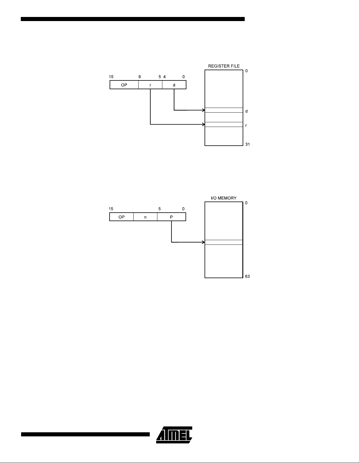
Register Direct, Single Register Rd
Figure 8. Direct Single-register Addressing
The operand is contained in register d (Rd).
Register Indirect
Figure 9. Indirect Register Addressing
REGISTER FILE
Z-register
The register accessed is the one pointed to by the Z-register (R31, R30).
0
30
31
10
ATtiny10/11/12
ATtiny10/11/12
Register Direct, Two Registers Rd and Rr
Figure 10. Direct Register Addressing, Two Registers
Operands are contained in register r (Rr) and d (Rd). The result is stored in register d (Rd).
I/O Direct
Figure 11. I/O Direct Addressing
Operand address is contained in 6 bits of the instruction word. n is the destination or source register address.
11
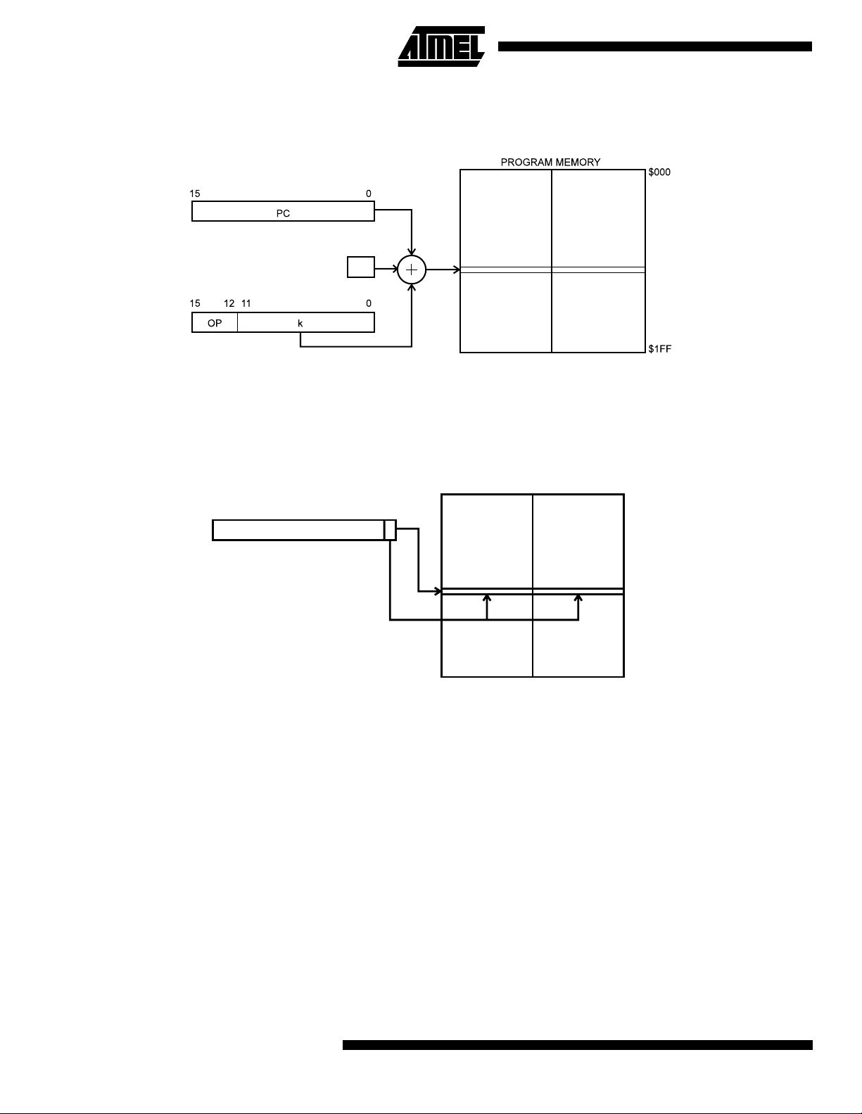
Relative Program Addressing, RJMP and RCALL
Figure 12. Relative Program Memory Addressing
+1
Program execution continues at address PC + k + 1. The relative address k is -2048 to 2047.
Constant Addressing Using the LPM Instruction
Figure 13. Code Memory Constant Addressing
PROGRAM MEMORY
15 1 0
Z-REGISTER
$000
$1FF
Constant byte address is specified by the Z-register contents. The 15 MSBs select word address (0 - 511), the LSB selects
low byte if cleared (LSB = 0) or high byte if set (LSB = 1).
Subroutine and Interrupt Hardware Stack
The ATtiny10/11 /12 uses a 3 -le vel-d eep hardw are stac k f or su brou tines and inter rup ts. The ha rdwa re sta ck is 9 bi ts w ide
and stores the program counter (PC) return address while subroutines and interrupts are executed.
RCALL instructions and interrupts push the PC return address onto stack level 0, and the data in the other stack levels 1-2
are pushed one level deeper in the stack. When a RET or RETI instruction is executed the returning PC is fetched from
stack level 0, and the data in the other stack levels 1-2 are popped one level in the stack.
If more than three subsequent su brouti ne calls or interrupt s are exec uted, the fi rst valu es written to the stack are overwr itten. Pushing four ret urn ad dr es ses A 1, A 2, A3 a nd A 4, fo ll owed by fou r sub ro utine or interrupt returns, will pop A 4, A3, A 2
and once more A2 from the hardware stack.
12
ATtiny10/11/12

ATtiny10/11/12
EEPROM Data Memory
The ATtiny12 contains 64 b yte s o f data EE PRO M m emo ry . It is o rg ani ze d as a sepa ra te da ta sp ac e, i n whi ch singl e by tes
can be read and written. The EEPROM has an endur ance of at least 100, 000 write /erase cy cles. The acces s betwee n the
EEPROM and the CPU is de scrib ed on pag e 33, sp ecifyin g the EE PROM Addres s Regis ter, th e EEPRO M Data Reg ister ,
and the EEPROM Control Register.
For SPI data downloading, see “Memory Programming ” on page 39 for a detailed description.
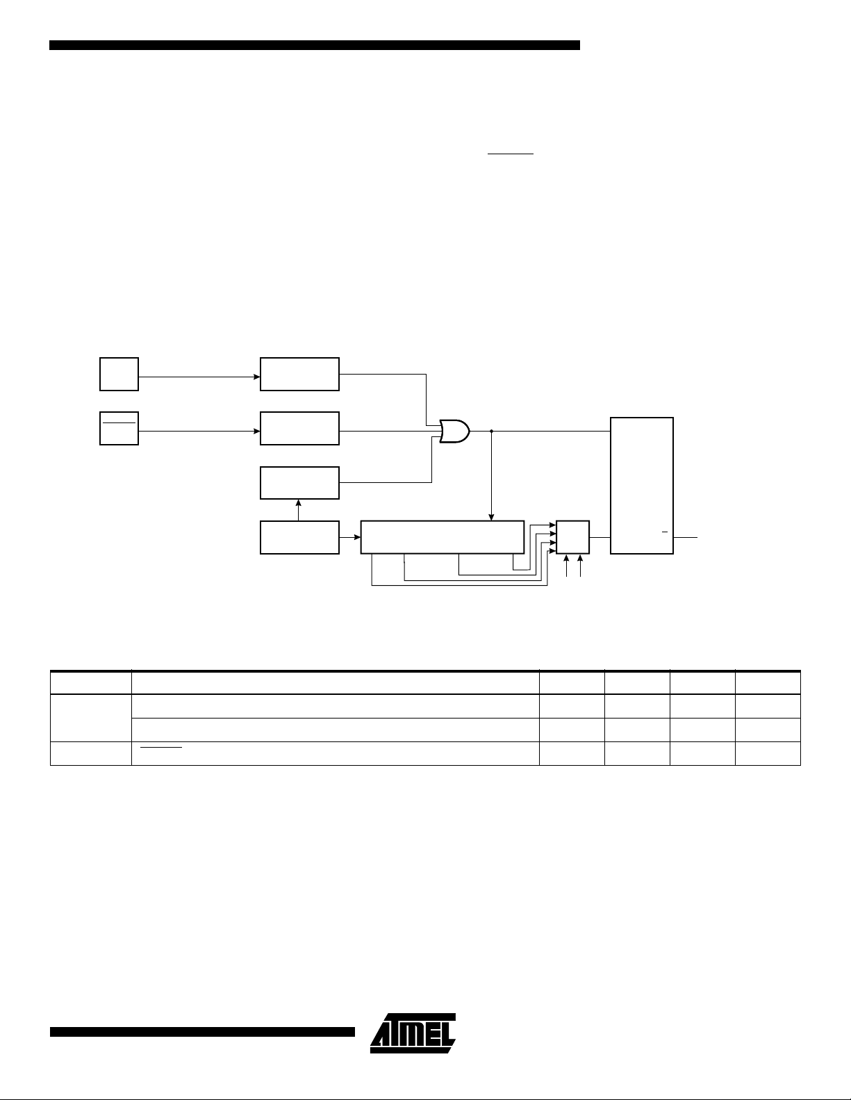
Memory Access and Instruction Execution Timing
This section describes the general access timing concepts for instruction execution and internal memory access.
The AVR CPU is driven by the System Clock Ø, directly generated from the external clock c rystal for the c hip. No interna l
clock division is used.
Figure 14 shows the parallel instruction fetches and instructio n executions enabled by the Harvard architecture and the
fast-access register file concept. This is the basic pipelining concept to obtain up to 1 MIPS per MHz with the corresponding
unique results for functions per cost, functions per clocks, and functions per power-unit.
Figure 14. The Parallel Instruction Fetches and Instruction Executions
T1 T2 T3 T4
System Clock Ø
1st Instruction Fetch
1st Instruction Execute
2nd Instruction Fetch
2nd Instruction Execute
3rd Instruction Fetch
3rd Instruction Execute
4th Instruction Fetch
Figure 15 shows the internal timing concept for the register file. In a single clock cycle, an ALU operation using two register
operands is executed and the result is stored back to the destination register.
Figure 15. Single-cycle ALU Operation
T1 T2 T3 T4
System Clock Ø
Total Execution Time
Register Operands Fetch
ALU Operation Execute
Result Write Back
13

I/O Memory
The I/O space definition of the ATtiny10/11/12 is shown in the following table:
Table 4. ATtiny10/11/12 I/O Space
Address Hex Name Device Function
$3F SREG ATtiny10/11/12 Status Register
$3B GIMSK ATtiny10/11/12 General Interrupt Mask Register
$3A GIFR ATtiny10/11/12 General Interrupt Flag Register
$39 TIMSK ATtiny10/11/12 Timer/Counter Interrupt Mask Register
$38 TIFR ATtiny10/11/12 Timer/Counter Interrupt Flag Register
$35 MCUCR ATtiny10/11/12 MCU Control Register
$34 MCUSR ATtiny10/11/12 MCU Status Register
$33 TCCR0 ATtiny10/11/12 Timer/Counter0 Control Register
$32 TCNT0 ATtiny10/11/12 Timer/Counter0 (8-bit)
$31 OSCCAL ATtiny12 Oscillator Calibration Register
$21 WDTCR ATtiny10/11/12 Watchdog Timer Control Register
$1E EEAR ATtiny12 EEPROM Address Register
$1D EEDR ATtiny12 EEPROM Data Register
$1C EECR ATtiny12 EEPROM Control Register
$18 PORTB ATtiny10/11/12 Data Register, Port B
$17 DDRB ATtiny10/11/12 Data Direction Register, Port B
$16 PINB ATtiny10/11/12 Input Pins, Port B
$08 ACSR ATtiny10/11/12 Analog Comparator Control and Status Register
Note: Reserved and unused locations are not shown in the table.
All the different ATtiny10/11/12 I/O and peripherals are placed in the I/O space. The different I/O locations are accessed by
the IN and OUT instructions transferring data between the 32 general-purpose working registers and the I/O space. I/O registers within the addr ess ran ge $00 - $1F ar e direc tly b it-acces sible us ing th e SBI and CBI instruc tions . In these regis ters,
the value of sing le bits can be checked by using the SBIS and SBIC inst ruct ions. Refer to the Instruct ion Se t S umm ar y for
more details.
For compatibility wi th fu tur e de vi ce s, re se rv ed bit s s ho uld be wr i tten to z ero i f ac ce ss ed . Res er v ed I/ O m emo ry ad dr es se d
should never be written.
The different I/O and peripherals control registers are explained in the following sections.
Status Register – SREG
The AVR status register (SREG) at I/O space location $3F is defined as:
Bit 76543210
$3F I T H S V N Z C SREG
Read/Write R/W R/W R/W R/W R/W R/W R/W R/W
Initial value 0 0 0 0 0 0 0 0
Bit 7 - I: Global Interrupt Enable
•
The global interrup t enable bit must be set (one) for the interrup ts to be enable d. The indivi dual inter rupt enab le control is
then performed in sep arate contr ol registe rs. If the gl obal interru pt enable r egister is cleared (ze ro), none of the interrupts
14
ATtiny10/11/12

ATtiny10/11/12
are enabled independent of the individual interrupt enable settings. The I-bit is cleared by hardware after an interrupt has
occurred, and is set by the RETI instruction to enable subsequent interrupts.
Bit 6 - T: Bit Copy Storage
•
The bit copy instruc tions B LD (Bit L oaD) a nd BST (Bit ST ore) u se the T-bit a s sour ce and destinati on for the op erated bi t.
A bit from a register in the registe r file ca n be co pied into T by the BST instruction, and a bit in T can be cop ied into a bi t in
a register in the register file by the BLD instruction.
Bit 5 - H: Half Carry Flag
•
The half carry flag H indicates a half-carry in some arithmetic operations. See the Instruction Set description for detailed
information.
Bit 4 - S: Sign Bit, S = N ⊕ V
•
The S-bit is always an exclusive or between the negative flag N and the two’s complement overflow flag V. See the Instruction Set description for detailed information.
•
Bit 3 - V: Two’s Complement Overflow Flag
The two’s complement overflow flag V supports two’s com plement arithmetic. S ee the Instruction S et description for
detailed information.
•
Bit 2 - N: Negative Flag
The negative flag N indicates a negative result from an arithmetical or logical operation. See the Instruction Set description
for detailed information.
Bit 1 - Z: Zero Flag
•
The zero flag Z indicates a zero result from an arithmetical or logical operation. See the Instruction Set description for
detailed information.
Bit 0 - C: Carry Flag
•
The carry flag C indicates a carry in an a rithmetical or logical ope ration. See the Ins truction Set des cription for d etailed
information.
Note that the status register is not automatically stored when entering an interrupt routine and restored when returning from
an interrupt routine. This must be handled by software.
Reset and Interrupt Handling
The ATtiny10/11 provides four different interrupt sources and the ATtiny12 provides five. These interrupts and the separate
reset vector each hav e a se par at e pr ogram vector in the program memory spac e. A ll t he in terr upts are as si gn ed in div i dua l
enable bits which must be set (one) together with the I-bit in the status register in order to enable the interrupt.
The lowest addresses i n the pro gram memo ry space are automatica lly defined a s the Rese t and Inter rupt vector s. The
complete list of vectors is shown in Table 5. The list also determines the priority levels of the different interrupts. The lower
the address, the higher the priority level. RESET has the highest priority, and next is INT0 – the External Interrupt Request
0, etc.
15

Table 5. Reset and Interrupt Vectors
Vector No. Device Program Address Source Interrupt Definition
1 ATtiny10/11 $000 RESET
External Pin, Power-on Reset and
Watchdog Reset
1 ATtiny12 $000 RESET
External Pin, Power-on Reset, Brown-out
Reset and Watchdog Reset
2 ATtiny10/11/12 $001 INT0 External Interrupt Request 0
3 ATtiny10/11/12 $002 I/O Pins Pin Change Interrupt
4 ATtiny10/11/12 $003 TIMER0, OVF0 Timer/Counter0 Overflow
5 ATtiny10/11 $004 ANA_COMP Analog Comparator
5 ATtiny12 $004 EE_RDY EEPROM Ready
6 ATtiny12 $005 ANA_COMP Analog Comparator
The most typical and general program setup for the reset and interrupt vector addresses for the ATtiny10/11 are:
Address Labels Code Comments
$000 rjmp RESET ; Reset handler
$001 rjmp EXT_INT0 ; IRQ0 handler
$002 rjmp PIN_CHANGE ; Pin change handler
$003 rjmp TIM0_OVF ; Timer0 overflow handler
$004 rjmp ANA_COMP ; Analog Comparator handler
;
$005 MAIN: <instr> xxx ; Main program start
… … … …
The most typical and general program setup for the reset and interrupt vector addresses for the ATtiny12 are:
Address Labels Code Comments
$000 rjmp RESET ; Reset handler
$001 rjmp EXT_INT0 ; IRQ0 handler
$002 rjmp PIN_CHANGE ; Pin change handler
$003 rjmp TIM0_OVF ; Timer0 overflow handler
$004 rjmp EE_RDY ; EEPROM Ready handler
$005 rjmp ANA_COMP ; Analog Comparator handler
;
$006 MAIN: <instr> xxx ; Main program start
… … … …
16
ATtiny10/11/12
ATtiny10/11/12
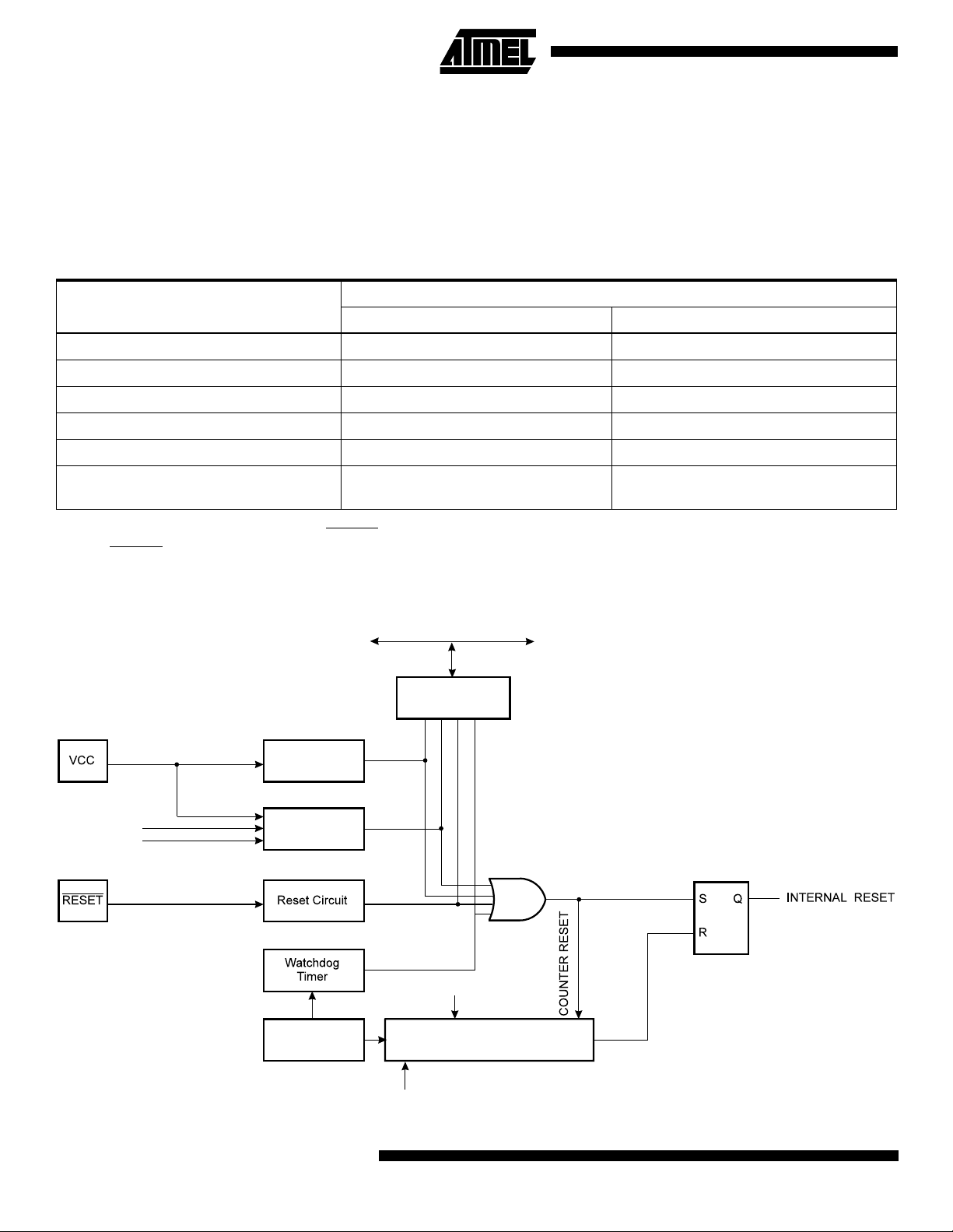
Reset Sources
The ATtiny10/11/12 provides three or four sources of reset:
• Power-on Reset. The MCU is reset when the supply voltage is below the power-on reset threshold (V
• External Reset. The MCU is reset when a low level is present on the RESET pin for more than 50 ns.
• Watchdog Reset. The MCU is reset when the Watchdog timer period expires and the Watchdog is enabled.
• Brown-out Reset. The MCU is reset when the supply voltage V
falls below a certain voltage (ATtiny12 only).
CC
During reset, all I/O regist ers are the n set to their ini tial valu es, and the pro gram starts execution from address $000. The
instruction pla ced in addr ess $000 m ust be an RJM P – relat ive ju mp – ins tructi on to the rese t han dling routi ne. If the program never enables an interrupt sour ce, the interrupt v ectors are not used, a nd regular progr am code can be pl aced at
these locations. The circuit diagram in Figure 16 shows the reset logic for the ATtiny10/11. Figure 17 shows the reset logic
for the ATtiny12. Table 6 def ine s th e el ec tric al param eter s of the reset circuitry for ATtiny10/11. T ab le 8 sh ows the p ar ameters of the reset circuitry for ATtiny12.
Figure 16. Reset Logic for the ATtiny10/11
VCC
Power-on Reset
Circuit
POR
POT
).
RESET
Reset Circuit
Watchdog
Timer
On-chip
RC Oscillator
COUNTER RESET
20-stage Ripple Counter
Q3 Q19
Q9
Q13
CKSEL
FSTRT
QS
INTERNAL
R
Q
RESET
Table 6. Reset Characteristics for the ATtiny10/11
Symbol Parameter Min Typ Max Units
(1)
V
POT
V
RST
Note: 1. The Power-on Reset will not work unless the supply voltage has been below V
Power-on Reset Threshold Voltage (rising) 1.0 1.4 1.8 V
Power-on Reset Threshold Voltage (falling) 0.4 0.6 0.8 V
RESET Pin Threshold Voltage 0.6 V
(falling).
POT
CC
V
17
Power-on Reset for the ATtiny10/11
A Power-on Reset (POR) circuit ensures that the device is reset from power-on. As shown in Figure 16, an internal timer is
clocked from the watchdog timer. Thi s timer prevents the MCU from starting a cer tain period after V
Power-on Threshold Voltage – V
. See Figure 18. The total reset period is the Delay Time-out period – t
POT
has reached the
CC
. The FSTRT
TOUT
fuse bit in the Flash can be programmed to give a shorter start-up time.The start-up times for the different clock options are
shown in the follo wing ta ble. T he Wa tchdog Oscill ator i s used for t iming the st art-up time, a nd t his osc illator is voltag e
dependent as shown in the section “ATtiny11 Typical Characteristics” on page 54.
Table 7. Start-up Times for the ATtiny10/11 (V
Selected Clock Option
= 2.7V)
CC
Start-up Time t
TOUT
FSTRT Unprogrammed FSTRT Programmed
External Crystal 67 ms 4.2 ms
External Ceramic Resonator 67 ms 4.2 ms
External Low-frequency Crystal 4.2 s 4.2 s
External RC Oscillator 4.2 ms 67 µs
Internal RC Oscillator 4.2 ms 67 µs
External Clock 4.2 ms
If the built-in start-up delay is sufficient, RESET
ing the RESET
pin low for a period after VCC has been applied, the Power-on Reset period can be extended. Refer to
can be connected to VCC directly or via an external pull-up resistor. By hold-
5 clocks from reset,
2 clocks from powe r-down
Figure 19 for a timing example on this.
Figure 17. Reset Logic for the ATtiny12
DATA BUS
MCU Status
Register (MCUSR)
BODEN
BODLEVEL
18
Power-on Reset
Circuit
Brown-out
Reset Circuit
On-chip
RC Oscillator
ATtiny10/11/12
CK
BORF
PORF
CKSEL[3:0]
WDRF
EXTRF
Delay Counters
Full
ATtiny10/11/12
Table 8. Reset Characteristics for the ATtiny12
Symbol Parameter Condition Min Typ Max Units
Power-on Reset Threshold Voltage
(1)
V
POT
(rising)
Power-on Reset Threshold Voltage
(falling)
BOD disabled 1.0 1.4 1.8 V
BOD enabled 0.6 1.2 1.8 V
BOD disabled 0.4 0.6 0.8 V
BOD enabled 0.6 1.2 1.8 V
V
RST
RESET Pin Threshold Voltage 0.6V
CC
(BODLEVEL = 1) 1.7 1.8 1.9
V
BOT
Note: 1. The Power-on Reset will not work unless the supply voltage has been below V
Brown-out Reset Threshold Voltage
(BODLEVEL = 0) 2.6 2.7 2.8
(falling).
POT
Table 9. ATtiny12 Clock Options and Start-up Times
Start-up Time, V
CKSEL3..0 Clock Source
1111 Ext. Crystal/Ceramic Resonator
1110 Ext. Crystal/Ceramic Resonator
1101 Ext. Crystal/Ceramic Resonator
(1)
(1)
(1)
BODLEVEL Unprogrammed
3.6 ms + 1K CK 4.2 ms + 1K CK
1100 Ext. Crystal/Ceramic Resonator 16K CK 16K CK
1011 Ext. Crystal/Ceramic Resonator 3.6 ms + 16K CK 4.2 ms + 16K CK
1010 Ext. Crystal/Ceramic Resonator 57 ms + 16K CK 67 ms + 16K CK
1001 Ext. Low-frequency Crystal 57 ms + 1K CK 67 ms + 1K CK
1000 Ext. Low-frequency Crystal 57 ms + 32K CK 67 ms + 32K CK
0111 Ext. RC Oscillator 6 CK 6 CK
0110 Ext. RC Oscillator 3.6 ms + 6 CK 4.2 ms + 6 CK
= 1.8V,
CC
Start-up Time, VCC = 2.7V,
BODLEVEL Programmed
1K CK 1K CK
57 ms 1K CK 67 ms + 1K CK
V
V
0101 Ext. RC Oscillator 57 ms + 6 CK 67 ms + 6 CK
0100 Int. RC Oscillator 6 CK 6 CK
0011 Int. RC Oscillator 3.6 ms + 6 CK 4.2 ms + 6 CK
0010 Int. RC Oscillator 57 ms + 6 CK 67 ms + 6 CK
0001 Ext. Clock 6 CK 6 CK
0000 Ext. Clock 3.6 ms + 6 CK 4.2 ms + 6 CK
Note: 1. Due to the limited number of clock cycles in the start-up period, it is recommended that Ceramic Resonator be used.
This table shows the start-up times from reset. From sleep, only the clock counting part of the start-up time is used. The
Watchdog oscillator is used for ti min g th e r eal -tim e part of the start-up time. Th e nu mbe r of WD T os ci ll ato r cy c les us ed for
each time-out is shown in Table 10.
19

Table 10. Number of Watchdog Oscillator Cycles
BODLEVEL Time-out Number of Cycles
Unprogrammed 3.6 ms (at V
Unprogrammed 57 ms (at V
Programmed 4.2 ms (at V
= 1.8V) 256
cc
= 1.8V) 4K
cc
= 2.7V) 1K
cc
Programmed 67 ms (at Vcc = 2.7V) 16K
The frequency of the watch dog osc illator is voltag e depe ndent as shown in the sect ion “A Ttiny 11 T ypic al Chara cter ist ics”
on page 54.
Note that the BODLEVEL fuse c an be us ed to s elec t st ar t- up times ev en i f the Brown- o ut Dete ct ion is dis ab led (by l eav in g
the BODEN fuse unprogrammed).
The device is shipped with CKSEL3..0 = 0010.
Power-on Reset for the ATtiny12
A Power-on Reset (POR) pulse is generated by an on-ch ip detection circuit. The de tection level is nominally 1.4V. The
POR is activated whenever V
is below the detection level. The POR circuit can be used to trigger the start-up reset, as
CC
well as detect a failure in supply voltage.
The Power-on Reset (POR) circuit ensures that the device is reset from power-on. Reaching the Power-on Reset threshold
voltage invokes a de la y c oun ter , wh ic h de ter mi nes the delay for which the device is ke pt i n Re set after V
rise. The time-
CC
out period of the del ay cou nter can be defined by the user t hr ough the CKS EL fuses . T he dif fer ent se lec ti ons for th e de lay
period are presented in Table 9. The Reset signal is activated again, without any delay, when the V
decreases below
CC
detection level.
If the built-in start-up delay is sufficient, RESET
Figure 18. By holding the RESET
pin low for a period after VCC has been applied, the Power-on Reset period can be
can be connected to VCC directly or via an external pull-up resistor. See
extended. Refer to Figure 19 for a timing example on this.
Figure 18. MCU Start-up, RESET
V
CC
RESET
TIME-OUT
INTERNAL
RESET
Tied to VCC.
V
POT
V
RST
t
TOUT
20
ATtiny10/11/12

ATtiny10/11/12
Figure 19. MCU Start-up, RESET
V
CC
RESET
TIME-OUT
INTERNAL
RESET
Extended Externally
V
POT
V
RST
t
TOUT
External Reset
An external reset is generated by a low level on the RESET
pin. Reset pulses longer than 50 ns will generate a reset, even
if the clock is no t running. Shorter pu lses are n ot guarante ed to gener ate a re set. When the applied s ignal reac hes the
Reset Threshold Voltage – V
– on its positive edge, the delay timer starts the MCU after the Time-out period (t
RST
TOUT
) has
expired.
Figure 20. External Reset during Operation
V
CC
RESET
TIME-OUT
INTERNAL
RESET
V
RST
t
TOUT
Brown-out Detection (ATtiny12)
ATtiny12 has an on-chi p brown-out dete ction (BOD ) circuit for monit oring the V
circuit can be enabled/disabled by the fuse BODEN. When BODEN is enabled (BODEN programmed), and V
below the trigger level, the brown-out reset is immediately activated. When V
level during the opera tion. The BOD
CC
increases above the trigger level, the
CC
decreases
CC
brown-out reset is de ac tiv ate d af ter a d el ay. T he d el ay is de fin ed b y the u se r in the sa me w ay as the del ay of PO R sig nal ,
in Table 5. The trigger level for the BOD can be selected by the fuse BODLEVEL to be 1.8V (BODLEVEL unprogrammed),
or 2.7V (BODLEVEL programmed). The trigger level has a hysteresis of 50 mV to ensure spike-free brown-out detection.
The BOD circuit will only detect a drop in V
if the voltage stays below the trigger level for longer than 7 µs for trigger level
CC
2.7V, 24 µs for trigge r level 1.8V (typical values).
21
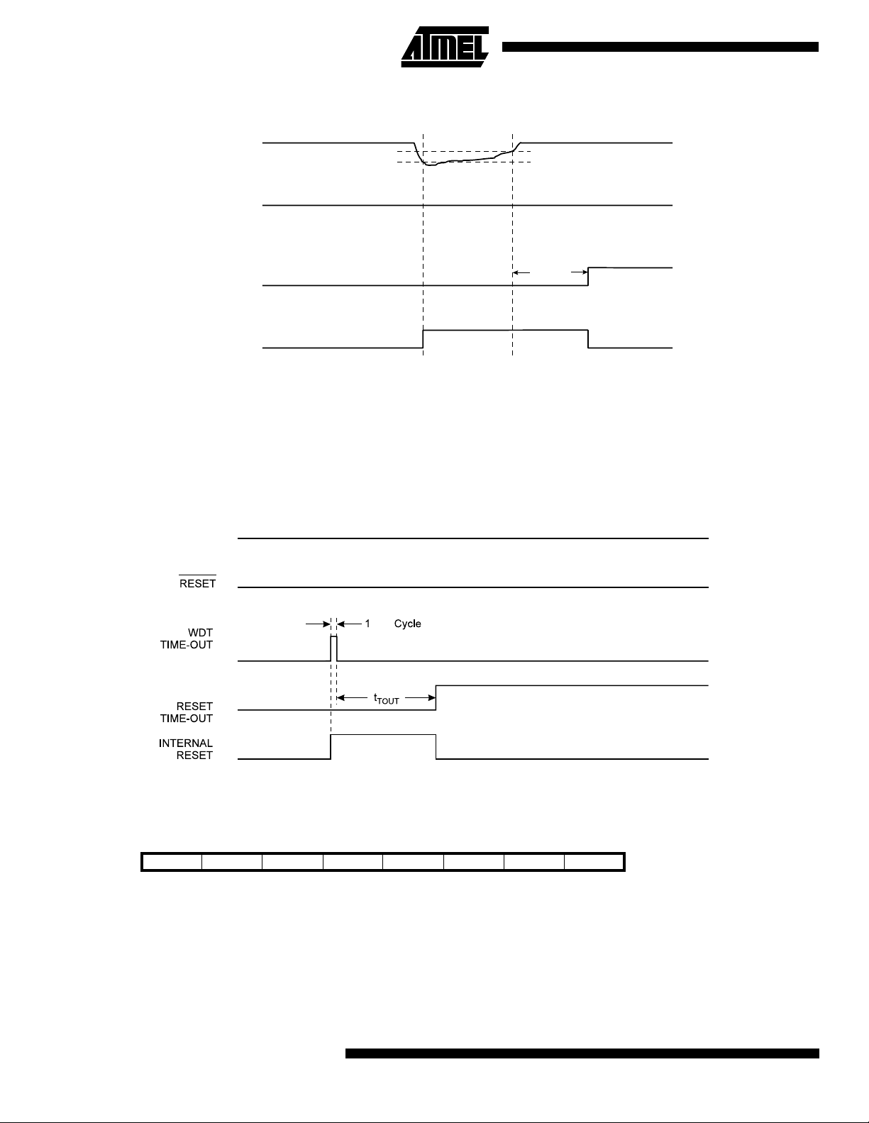
Figure 21. Brown-out Reset during Operation (ATtiny12)
V
CC
V
BOT-
V
BOT+
RESET
t
TIME-OUT
TOUT
INTERNAL
RESET
Note: The hy steresis on V
BOT
: V
BOT +
= V
+ 25 mV, V
BOT
BOT-
= V
BOT
- 25 mV.
Watchdog Rese t
When the Watchdog tim es out , it wil l gene rate a s hor t res et pul se of 1 CK cy c le dur at ion . O n th e fa ll ing ed ge o f thi s pul s e,
the delay timer starts counting the Time-out period (t
). Refer to page 31 for details on operation of the Watchdog.
TOUT
Figure 22. Watchdog Reset during Operatio n
V
CC
CK
MCU Status Register – MCUSR of the ATtiny10/11
The MCU Status Register provides information on which reset source caused an MCU reset.
Bit 76543210
$34 ------EXTRFPORFMCUSR
Read/Write R R R R R R R/W R/W
Initial value 0 0 0 0 0 0 See bit description
Bit 7..2 - Res: Reserved Bits
•
These bits are reserved bits in the ATtiny10/11 and always read as zero.
Bit 1 - EXTRF: EXTernal Reset Flag
•
After a power-on reset, this bit is undefined (X). It will be set by an external reset. A watchdog reset will leave this bit
unchanged.
22
ATtiny10/11/12
ATtiny10/11/12
Bit 0 - PORF: Power-on Reset Flag
•
This bit is set by a power-on reset. A watchdog reset or an external reset will leave this bit unchanged.
To summarize, the following table shows the value of these two bits after the three modes of reset.
Table 11. PORF and EXTRF Values after Reset
Reset Source EXTRF PORF
Power-on undefined 1
External Reset 1 unchanged
Watchdog Reset unchanged unchanged
To identify a reset condition, the user software should clear both the PORF and EXTRF bits as early as possible in the program. Checking the PORF and EXTRF values is done before the bits are cleared. If the bit is cleared before an external or
watchdog reset occurs, the source of reset can be found by using the following truth table:
Table 12. Reset Source Identification
EXTRF PORF Reset Source
0 0 Watchdog Re set
1 0 External Reset
0 1 Power-on Reset
1 1 Power-on Reset
MCU Status Register – MCUSR for the ATtiny12
The MCU Status Register provides information on which reset source caused an MCU reset.
Bit 76543210
$34 - - - - WDRF BORF EXTRF PORF MCUSR
Read/Write R R R R R/W R/W R/W R/W
Initial value 0 0 0 0 See bit description
Bit 7..4 - Res: Reserved Bits
•
These bits are reserved bits in the ATtiny12 and always read as zero.
Bit 3 - WDRF: Watchdog Reset Flag
•
This bit is set if a watchdog reset occurs. The bit is reset by a power-on reset, or by writing a logic zero to the flag.
Bit 2 - BORF: Brown-out Reset Flag
•
This bit is set if a brown-out reset occurs. The bit is reset by a power-on reset, or by writing a logic zero to the flag.
•
Bit 1 - EXTRF: EXTernal Reset Flag
This bit is set if an external reset occurs. The bit is reset by a power-on reset, or by writing a logic zero to the flag.
Bit 0 - PORF: Power-on Reset Flag
•
This bit is set if a power-on reset occurs. The bit is reset by writing a logic zero to the flag.
To use the reset flags to iden tify a res et c ondi ti on, th e user sho ul d read an d the n re se t the MC USR as early as possible in
the program. If the re gister is c leared bef ore anot her reset oc curs, the source of th e reset ca n be found by examinin g the
reset flags.
ATtiny12 Interna l Voltage Reference
ATtiny12 features an internal voltage reference with a nominal voltage of 1.22V. This reference is used for Brown-out
Detection, and it can be used as an input to the Analog Comparator.
23

Voltage Reference Enable Signals and Start-up Time
The voltage reference has a start-up time that may influence the way it should be used. The maximum start-up time is TBD.
To save power, the reference is not always turned on. The reference is on during the following situations:
1. When BOD is enabled (by programming the BODEN fuse)
2. When the bandgap reference is connected to the Analog Comparator (by setting the AINBG bit in ACSR)
Thus, when BOD is not enabled, after setting the AINBG bit, the user must always allow the reference to start up before the
output from the Analog Compara tor is used. The bandgap refe rence use s approxi matel y 10 µA, and to reduc e power consumption in Power-down mode, the user can turn off the reference when entering this mode.
Interrupt Handling
The ATtiny10/11/12 h as two 8-bi t Interr upt Ma sk cont rol regist ers; G IMSK – Gene ral Interrup t Ma sk reg ister and TIMSK –
Timer/Counter Interrupt Mask register.
When an interrupt occurs, the Global Interrupt Enable I-bit is cleared (zero) and all interrupts are disabled. The user software can set (one) the I-bit to enabl e nested interrupts. The I-bit is set (one) when a Return from Interrupt instruction –
RETI – is executed.
When the Program Counter is vectored to the actual interrupt vector in order to execute the interrupt handling routine, hardware clears the corresponding flag that generated the interrupt. Some of the interrupt flags can also be cleared by writing a
logic one to the flag bit position(s) to be cleared.
If an interrupt condition occurs when the corresponding interrupt enable bit is cleared (zero), the interrupt flag will be set
and remembered until the interrupt is enabled, or the flag is cleared by software.
If one or more interrupt condi tions occu r when the global interrupt ena ble bit is clea red (zero), th e correspondi ng interrup t
flag(s) will be set and remembered until the global interrupt enable bit is set (one), and will be executed by order of priority.
Note that external level interrupt does not have a flag, and will only be remembered for as long as the interrupt condition is
active.
Note that the status register is not automatically stored when entering an interrupt routine and restored when returning from
an interrupt routine. This must be handled by software.
Interrupt Response Time
The interrupt execution response for all the enabled AVR interrupts is 4 clock cycles minimum. After the 4 clock cycles, the
program vector addr ess fo r the actual i nte rrup t ha ndl in g r ou tin e i s exec ute d. Du r ing thi s 4- c lock -cy cle period, the Program
Counter (9 bits) is pushed onto the Stack. The vector is normally a relative jump to the interrupt routine, and this jump takes
2 clock cycles. If an interrupt occurs during execution of a multi-cycle instruction, this instruction is completed before the
interrupt is served. In ATtiny12, if an interrupt occurs when the MCU is in Sleep mode, the interrupt response time is
increased by 4 clock cycles.
A return from an in terrupt h andli ng rou tine ta kes 4 cloc k cyc les. Du ring the se 4 c lock c ycles, the Pr ogram Co unte r (9 bits)
is popped back from th e St ac k, a nd th e I-fla g in SREG is se t. W hen AV R ex its fr om an i nterr upt , it wi ll al ways r et urn to the
main program and execute one more instruction before any pending interrupt is served.
General Interrupt Mask Register – GIMSK
Bit 7 6 5 4 3 2 1 0
$3B - INT0 PCIE - - - - - GIMSK
Read/Write R R/W R/W R R R R R
Initial value 0 0 0 0 0 0 0 0
Bit 7 - Res: Reserved Bit
•
This bit is a reserved bit in the ATtiny10/11/12 and always reads as zero.
Bit 6 - INT0: External Interrupt Request 0 Enable
•
When the INT0 bit is set (one) and the I-bit in the Status Register (SREG) is set (one), the external pin interrupt is enabled.
The Interrupt Sense Control0 bits 1/0 (ISC01 and ISC00) in the MCU general Control Register (MCUCR) define whether
the external interrupt is activated on rising or falling edge, on pin change, or low level of the INT0 pin. Activity on the pin will
24
ATtiny10/11/12
 Loading...