

Page 1

Features
• Utilizes the AVR
• High-performance and Low-power 8-bit RISC Architecture
– 90 Powerful Instructions – Most Single Clock Cycle Execution
– 32 x 8 General Purpose Working Registers
– Up to 8 MIPS Throughput at 8 MHz
• Nonvolatile Program and Data Memory
– 1K Byte of Flash Program Memory
In-System Programmable (ATtiny12)
Endurance: 1,000 Write/Erase Cycles (ATtiny11/12)
– 64 Bytes of In-System Programmable EEPROM Data Memory for ATtiny12
Endurance: 100,000 Write/Erase Cycles
– Programming Lock for Flash Program and EEPROM Data Security
• Peripheral Features
– Interrupt and Wake-up on Pin Change
– One 8-bit Timer/Counter with Separate Prescaler
– On-chip Analog Comparator
– Programmable Watchdog Timer with On-chip Oscillator
• Special Microcontroller Features
– Low-power Idle and Power-down Modes
– External and Internal Interrupt Sources
– In-System Programmable via SPI Port (ATtiny12)
– Enhanced Power-on Reset Circuit (ATtiny12)
– Internal Calibrated RC Oscillator (ATtiny12)
• Specification
– Low-power, High-speed CMOS Process Technology
– Fully Static Operation
• Power Consumption at 4 MHz, 3V, 25°C
– Active: 2.2 mA
– Idle Mode: 0.5 mA
– Power-down Mode: <1 µA
• Packages
– 8-pin PDIP and SOIC
• Operating Voltages
– 1.8 - 5.5V for ATtiny12V-1
– 2.7 - 5.5V for ATtiny11L-2 and ATtiny12L-4
– 4.0 - 5.5V for ATtiny11-6 and ATtiny12-8
• Speed Grades
– 0 - 1.2 MHz (ATtiny12V-1)
– 0 - 2 MHz (ATtiny11L-2)
– 0 - 4 MHz (ATtiny12L-4)
– 0 - 6 MHz (ATtiny11-6)
– 0 - 8 MHz (ATtiny12-8)
®
RISC Architecture
8-bit
Microcontroller
with 1K Byte
Flash
ATtiny11
ATtiny12
Pin Configur a t ion
ATtiny11
PDIP/SOIC
(RESET) PB5
(XTAL1) PB3
(XTAL2) PB4
GND
1
2
3
4
8
7
6
5
VCC
PB2 (T0)
PB1 (INT0/AIN1)
PB0 (AIN0)
(RESET) PB5
(XTAL1) PB3
(XTAL2) PB4
GND
ATtiny12
PDIP/SOIC
1
2
3
4
8
7
6
5
VCC
PB2 (SCK/T0)
PB1 (MISO/INT0/AIN1)
PB0 (MOSI/AIN0)
1006D–AVR–0 7/ 03
Rev. 1006D–AVR–07/03
1
Page 2

Description The ATtiny11/12 is a low-power CMOS 8-bit microcontroller based on the AVR RISC
architecture. By executing powerful instructions in a single clock cycle, the ATtiny11/12
achieves throug hputs a pproac hing 1 MIPS pe r MHz, all owing the syst em de signer to
optimize power consumption versus processing speed.
The AVR c ore c omb ines a r ich ins tructi on se t wi th 3 2 ge neral -purp ose wo rking regi sters. All the 32 regis ters are directly co nnected to the Ari thmetic Logic U nit (ALU),
allowing two independent registers to be accessed in one single instruction executed in
one clock cycle. The resulting architecture is more code efficient while achieving
throughputs up to ten times faster than conventional CISC microcontrollers.
Table 1. Parts Description
Device Flash EEPROM Register Voltage Range Frequency
ATtiny11L 1K - 32 2.7 - 5.5V 0-2 MHz
ATtiny11 1K - 32 4.0 - 5.5V 0-6 MHz
ATtiny12V 1K 64 B 32 1.8 - 5.5V 0-1.2 MHz
ATtiny12L 1K 64 B 32 2.7 - 5.5V 0-4 MHz
ATtiny12 1K 64 B 32 4.0 - 5.5V 0-8 MHz
ATtiny11 Block Diagram The ATtiny11 provides the following features: 1K bytes of Flash, up to five general-pur-
pose I/O lines, on e input line, 32 ge neral-purpose work ing registers, an 8-bit
timer/counter, internal and external interrupts, programmable W atchdog Timer w ith
internal oscillator, and two software-selectable power-saving modes. The Idle Mode
stops the CPU while allowing the timer/counters and interrupt system to continue functioning. The Power-d own M ode s aves th e regist er conte nts but freezes the o scillator,
disabling all other chip functions until the next interrupt or hardware reset. The wake-up
or interrupt on pin change features enable the ATtiny11 to be highly responsive to external events, still f eaturi ng the l owest power c onsumpt ion while in the power-down modes .
The device is manufactured using Atmel’s high-density nonvolatile memory technology.
By combining an RISC 8-bit CPU with Flash on a monolithic chip, the Atmel ATtiny11 is
a powerful mic rocontro ller that provide s a highly-fl exible and cost -effec tive solution to
many embedded control applications.
The ATtiny11 AVR is supported with a full suite of program and system development
tools including: macro assemblers, progra m debugger/s imulators, in-circuit emulators,
and evaluation kits.
2
ATtiny11/12
1006D–AVR–07/03
Page 3
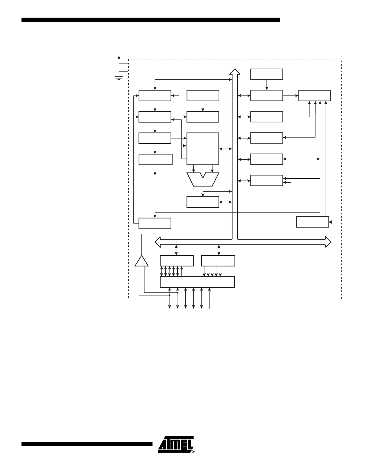
Figure 1. The ATtiny11 Block Diagram
VCC
GND
PROGRAM
COUNTER
STACK
POINTER
8-BIT DATABUS
INTERNAL
OSCILLATOR
WATCHDOG
TIMER
ATtiny11/12
TIMING AND
CONTROL
PROGRAM
FLASH
INSTRUCTION
REGISTER
INSTRUCTION
DECODER
CONTROL
LINES
PROGRAMMING
LOGIC
ANALOG
DATA REGISTER
ARATOR
COMP
+
PORTB
PORTB DRIVERS
HARDWARE
STACK
GENERALPURPOSE
REGISTERS
Z
ALU
STATUS
REGISTER
DATA DIR.
REG. PORTB
MCU CONTROL
REGISTER
MCU STATUS
REGISTER
TIMER/
COUNTER
INTERRUPT
UNIT
OSCILLATORS
1006D–AVR–07/03
PB0-PB5
3
Page 4

ATtiny12 Block Diagram Figure 2. The ATtiny12 Block Diagram
VCC
GND
PROGRAM
COUNTER
STACK
POINTER
8-BIT DATA BUS
INTERNAL
OSCILLATOR
WATCHDOG
TIMER
INTERNAL
CALIBRATED
OSCILLATOR
TIMING AND
CONTROL
PROGRAM
FLASH
INSTRUCTION
REGISTER
INSTRUCTION
DECODER
CONTROL
LINES
PROGRAMMING
LOGIC
ANALOG
DATA REGISTER
ARATOR
COMP
+
PORTB
PORTB DRIVERS
HARDWARE
STACK
GENERALPURPOSE
REGISTERS
Z
ALU
STATUS
REGISTER
SPI
DATA DIR.
REG. PORTB
MCU CONTROL
REGISTER
MCU STATUS
REGISTER
TIMER/
COUNTER
INTERRUPT
UNIT
EEPROM
OSCILLATORS
PB0-PB5
The ATtiny12 provides the following features: 1K bytes of Flash, 64 bytes EEPROM, up
to six general-purpose I/O lines, 32 general-purpose working registers, an 8-bit
timer/counter, internal and external interrupts, programmable W atchdog Timer w ith
internal oscillator, and two software-selectable power-saving modes. The Idle Mode
stops the CPU while allowing the timer/counters and interrupt system to continue functioning. The Power-d own M ode s aves th e regist er conte nts but freezes the o scillator,
disabling all other chip functions until the next interrupt or hardware reset. The wake-up
or interrupt on pin change features enable the ATtiny12 to be highly responsive to external events, still feat uring the lowest power consumpt ion while i n the power- down modes .
The device is manufactured using Atmel’s high-density nonvolatile memory technology.
By combining an RISC 8-bit CPU with Flash on a monolithic chip, the Atmel ATtiny12 is
a powerful mic rocontro ller that provide s a highly-fl exible and cost -effec tive solution to
many embedded control applications.
4
ATtiny11/12
1006D–AVR–07/03
Page 5

ATtiny11/12
The ATtiny12 AVR is supported with a full suite of program and system development
tools including: macro assemblers, progra m debugger/s imulators, in-circuit emulators,
and evaluation kits.
Pin Descriptions
VCC Supply voltage pin. GND Ground pin. Port B (PB5..PB0) Port B is a 6-bit I/O port. PB4..0 are I/O pins that can provide internal pull-ups (selected
for each bit). On ATtiny11, PB5 is input onl y. On ATtiny12, PB 5 is input or open-drain
output. The port p ins are t ri-stated w hen a res et con dition be comes a ctive, even if the
clock is not running. The use of pins PB5..3 as input or I/O pins is limited, depending on
reset and clock settings, as shown below.
Table 2. PB5..PB3 Functionality vs. Device Clocking Options
Device Clocking Option PB5 PB4 PB3
External Reset Enabled Used
External Reset Disabled Input
External Crystal - Used Used
(1)
(3)
(4)
/I/O
(2)
-
--
-
External Low-frequency Crystal - Used Used
External Ceramic Resonator - Used Used
External RC Oscillator - I/O
External Clock - I/O Used
Internal RC Oscillator - I/O I/O
Notes: 1. “Used” means the pin is used for reset or clock purposes.
2. “-” means the pin function is unaffected by the option.
3. Input means the pin is a port input pin.
4. On ATtiny11, PB5 is input only. On ATtiny12, PB5 is input or open-drain output.
5. I/O means the pin is a port input/output pin.
(5)
Used
XTAL1 Input to the inverting oscillator amplifier and input to the internal clock operating circuit. XTAL2 Output from the inverting oscillat or amplifier.
RESET
Reset input. An external reset is generated by a low level on the RESET pin. Reset
pulses longer than 50 ns will generate a reset, even if the clock is not running. Shorter
pulses are not guaranteed to generat e a reset.
Clock Options The device has the f ollowing clock source op tions, selectable by Flash fuse bit s as
shown:
Table 3. Device Clocking Options Select
1006D–AVR–07/03
Device Clocking Option ATtiny11 CKSEL2..0 ATtiny12 CKSEL3..0
External Crystal/Ceramic Resonator 111 1111 - 1010
External Low-frequency Crystal 110 1001 - 1000
External RC Oscillator 101 0111 - 0101
5
Page 6
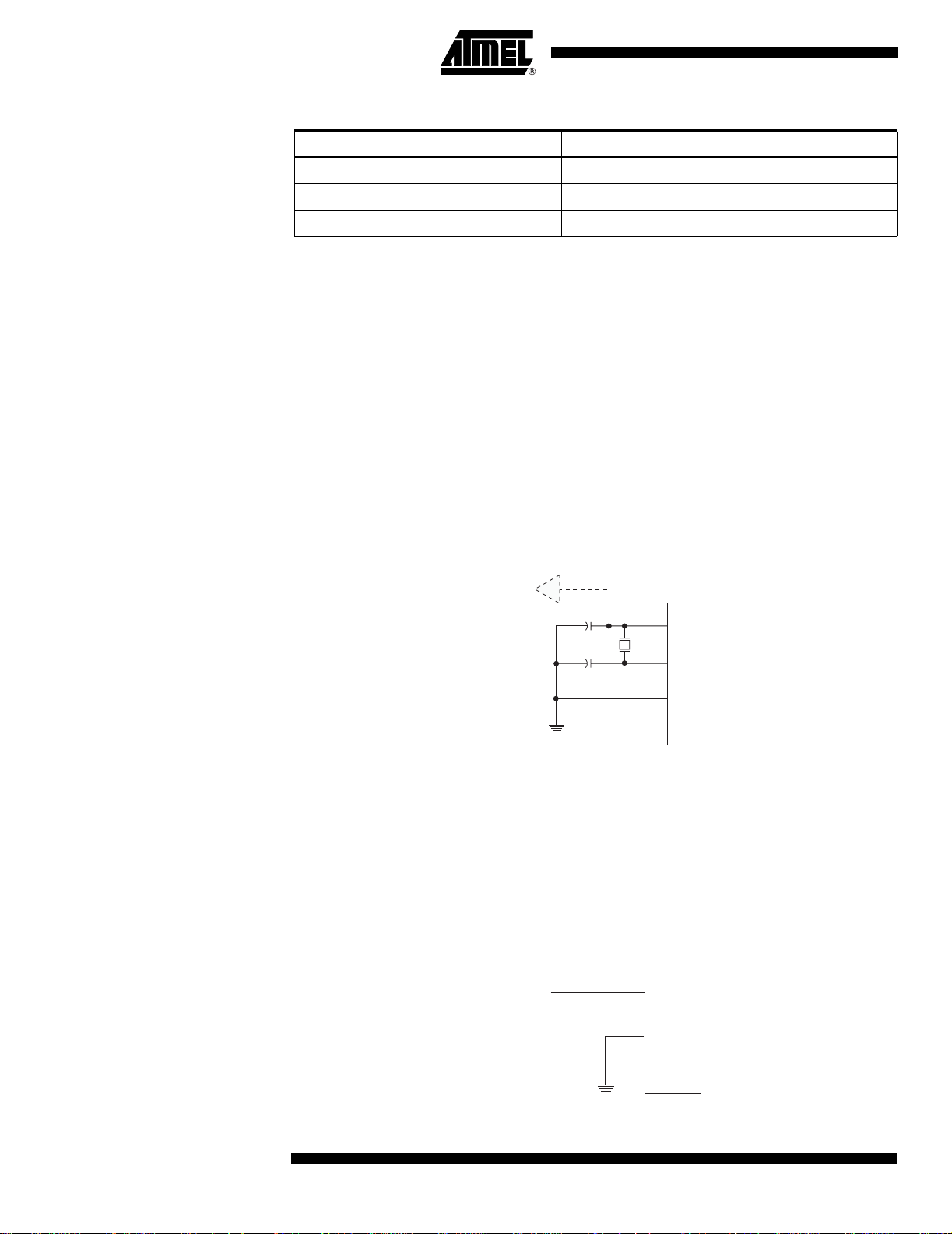
Table 3. Device Clocking Options Select (Continued)
Device Clocking Option ATtiny11 CKSEL2..0 ATtiny12 CKSEL3..0
Internal RC Oscillator 100 0100 - 0010
External Clock 000 0001 - 0000
Reserved Other Options -
Note: “1” means unprogrammed, “0” means programmed.
The various choices for ea ch clocking op tion give different start-u p times as shown in
Table 7 on page 18 and Table 9 on page 20.
Internal RC Oscillator The internal RC oscillator option is an on-chip oscil lat or running at a f ixed frequency of 1
MHz in ATtiny11 and 1.2 MHz in ATtiny12. If selected, the device can operate with no
external components. The device is shipped with this option selected. On ATtiny11, the
Watchdog Oscillator is used as a clock, while ATtiny12 uses a separate calibrated
oscillator.
Crystal Oscillator XTAL1 and XTAL2 are input and o utput , respectively, of an inverting amplifier which can
be configured for use as an on-chip oscillator, as shown in Figure 3. Either a quartz
crystal or a ceramic resonator may be used. Maximum frequency for crystal and resonators is 4 MHz. Minimum voltage for running on a low-frequency crystal is 2.5V.
Figure 3. Oscillator Connections
MAX 1 HC BUFFER
HC
C2
C1
Note: When using the MCU Oscillator as a clock for an external device, an HC buffer should be
connected as indicated in the figure.
XTAL2
XTAL1
GND
External Clock To drive the device from an external clock source, XTAL1 should be driven as shown in
Figure 4.
Figure 4. External Clock Drive Configurati on
PB4 (XTAL2)
EXTERNAL
OSCILLATOR
XTAL1
SIGNAL
GND
6
ATtiny11/12
1006D–AVR–07/03
Page 7

ATtiny11/12
External RC Oscillator For timing insensitive applications, the external RC configuration shown in Figure 5 can
be used. For details on how to choose R and C, see Table 29 on page 59. The external
RC oscillator is sensitive to noise from neigh boring pins, and to avoid proble ms, PB5
(RESET
put pin.
Figure 5. External RC Configuration
) should be used as an output or reset pin, and PB4 should be used as an out-
VCC
R
C
PB4 (XTAL2)
XTAL1
GND
1006D–AVR–07/03
7
Page 8

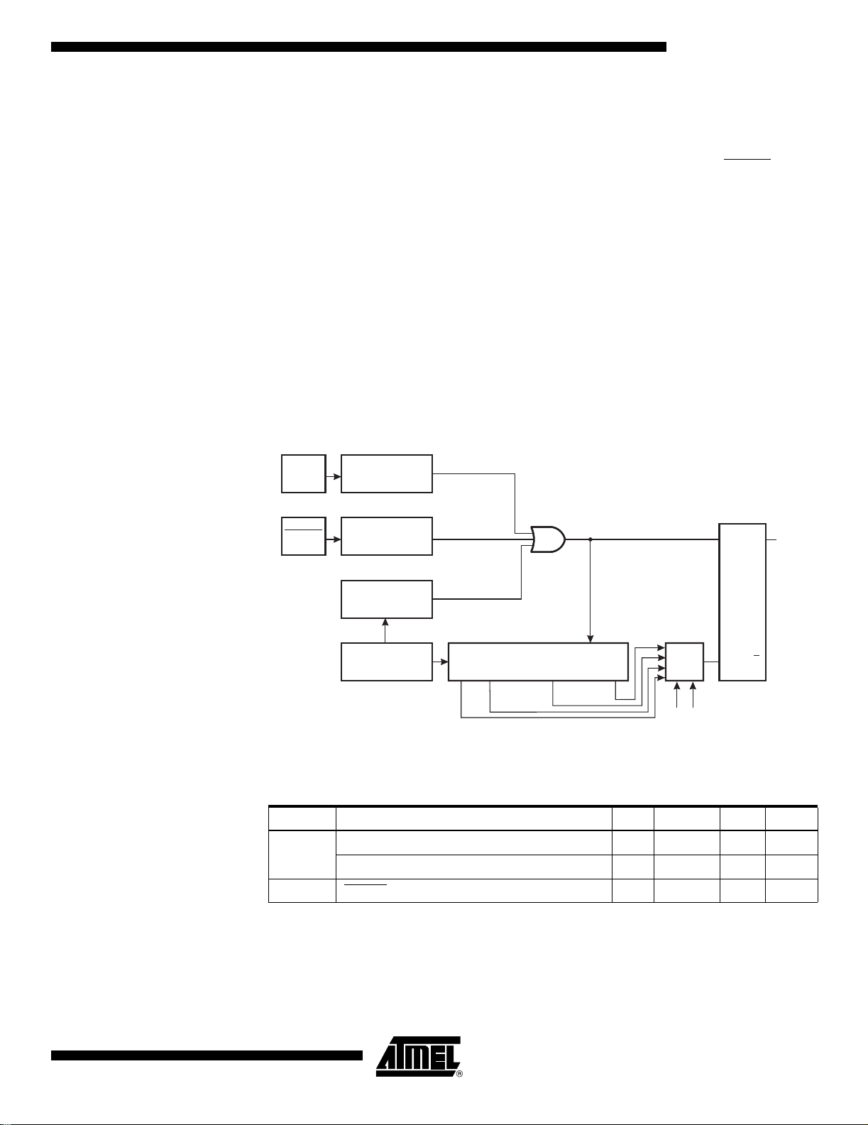
Architectural Overview
The fast-access register file concept contains 32 x 8-bit general-purpose working registers with a single-clock-cycle access time. This means that du ring one sing le clock
cycle, one ALU (Arithmetic Logic Unit) operation is executed. Two operands are output
from the register file, the operation is executed, and the result is stored back in the register file – in one clock cycle.
Two of the 32 registers can be used as a 16-bit pointer for indirect memory access. This
pointer is called the Z-pointer, and can address the register file and the Flash program
memory.
The ALU supp orts arithm etic and log ic fun ctions betwe en reg isters or b etween a co nstant and a register. Sin gle-register operati ons are also e xecuted in the A LU. Figure 2
shows the AT tiny1 1/12 AVR RISC mic rocont roller arc hitectu re. The A VR use s a Harvard architecture concept with separate memori es and buses for progra m and data
memories. The program memory is accessed with a two-stage pipelining. While one
instruction is being executed, the next instruction is pre-fetched from the program memory. This concept enables instructions to be executed in every clock cycle. The program
memory is reprogrammable Flash memory.
With the relative jump and relative call instructions, the whole 512 address space is
directly accessed. All A VR instructio ns have a single 16-bit word f ormat, mea ning that
every program memory address contains a single 16-bit instruction .
During interrupts and subroutine calls, the return address program counter (PC) is
stored on the stack . Th e stack i s a 3 -level-deep hardware stack de dicated for subroutines and interrupts.
The I/O memory space con tains 64 addresses f or CPU peri pheral functions as cont rol
registers, timer/counters, and other I/O functions. The memory spaces i n the AVR architecture are all linear and regular memory maps.
8
ATtiny11/12
1006D–AVR–07/03
Page 9

Figure 6. The ATtiny11/12 AVR RISC Architecture
8-bit Data Bus
ATtiny11/12
512 x 16
Program
Flash
Instruction
Register
Instruction
Decoder
Control Lines
Program
Counter
Direct Addressing
Status
and Test
32 x 8
General-
purpose
Registers
ALU
64 x 8 EEPROM
(ATtiny12 only)
Control
Registers
Interrupt
Unit
SPI Unit
(ATtiny12 only)
8-bit
Timer/Counter
Watchdog
Timer
Analog
Comparator
6
I/O Lines
A flexible inte rrupt modu le has its con trol regist ers in the I/O space with an additio nal
global interrupt enable bit in the status register. All the different interrupts have a separate interrupt vector in the interrupt vector tab le at the beginning of the
program memory. The different interrupts have priority in accordance with their interrupt
vector position. The lower the interrupt vector address, the higher the priority.
General-purpose Register File
1006D–AVR–07/03
Figure 7 shows the structure of the 32 general-purpose registers in the CPU.
Figure 7. AVR CPU General-purpose Working Registers
70
R0
R1
R2
General- …
purpose …
Working R28
Registers R29
R30 (Z-register low byte)
R31 (Z-r egister high byte)
All the register operating instructions in the instruction set have direct- and single-cycle
access to a ll regist ers. The only excepti on is the five c onstan t arithm etic an d logic
instructions SBCI, SUBI, CPI, ANDI, and ORI between a constant and a register and the
LDI instruction for load-immediate constant data. These instructions apply t o the second
half of the registe rs in the register f ile – R16..R 31. The genera l SBC, SU B, CP, AND,
9
Page 10

OR and all o ther op eration s bet ween two re gisters or on a si ngle reg ister apply to the
entire register file.
Registers 30 and 31 form a 16-bit pointer (the Z-pointer) which is used for indirect Flash
memory and register fil e access. When the register file is accessed, t he contents of R31
are discarded by the CPU.
ALU – Arithmetic Logic Unit
The high-performance AVR ALU operat es in d irect con nection with all the 32 gene ralpurpose working registers. Wit hin a sing le clock cycle , ALU op erations be tween registers in the register file are executed. The ALU operations are divided into three main
categories – arithmetic, logic and bit-functions. Some microcontrollers in the AVR product family feature a hardware multiplier in the arithmetic part of the ALU.
Flash Program Memory The ATtiny11/12 contain s 1K bytes on-chip Flash me mory for program storag e. Since
all instructions are single 16-bit words, the F lash is organized as 5 12 x 16 words. T he
Flash memory has an endurance of at least 1000 write/er ase cycles.
The ATtiny11/12 Program Counter is 9 bits wide, thus addressing the 512 words Flash
program memory.
See page 46 for a detailed description on Flash memory programming.
Program and Data Addressing Modes
Register Direct, Single Register Rd
The ATtiny11/12 AVR RISC Microcontroller supports powerful and efficient addressing
modes. This se ction describes the different addressin g modes supported i n the
ATtiny11/12. In the figures, OP means the ope ration code part of the instruction word.
To simplify, not all figure s show the exact location of the addressing bits.
Figure 8. Direct Single-register Addressing
10
The operand is contained in regist er d (Rd).
ATtiny11/12
1006D–AVR–07/03
Page 11

Register Indirect Figure 9. Indirect Register Addressing
ATtiny11/12
REGISTER FILE
0
The register accessed is the one pointed to by th e Z-register (R31, R30).
Register Direct, Two Registers
Figure 10. Direct Register Addressing, Two Registers
Rd and Rr
Operands are contained in register r (Rr) and d (Rd). The result is store d in regi ster d
(Rd).
I/O Direct Figure 11. I/O Direct Addressing
Z-register
30
31
1006D–AVR–07/03
Operand addres s is con taine d in 6 bit s of the instruc tion wor d. n is the desti natio n or
source register address.
11
Page 12

Relative Program Addr essing, RJMP and RCALL
Figure 12. Relative Program Memor y Addressing
+1
Program execution continues at address PC + k + 1. The relative address k is -2048 to
2047.
Constant Addressing Using the LPM Instruction
Subroutine and Interrupt Hardware Stack
Figure 13. Code Memory Constant Addressing
PROGRAM MEMORY
15 1 0
Z-REGISTER
$000
$1FF
Constant byte address is specified by the Z-register contents. The 15 MSBs select word
address (0 - 511) , the LSB sel ects low byte i f cleare d (LSB = 0) or hi gh byte if set
(LSB = 1).
The ATtiny11/12 uses a 3-level -deep hardwar e st ack for subr outin es and inter rupts. The
hardware stack is 9 bits wide and stores the program counter (PC) return address while
subroutines and inter rupt s are executed.
RCALL instructi ons an d int errupts pu sh th e PC return a ddress o nto stack l evel 0, a nd
the data in the other stack levels 1-2 are pushed one level deeper in the stack. When a
RET or RETI instruction is executed the returning PC is fetched from stack level 0, and
the data in the other stack level s 1-2 are popped one level in the stack.
12
If more than three subsequent subroutine calls or interrupts are executed, the first values written to the stack are overwritten. Pushing four return addresses A1, A2, A3, and
A4, followed by four subroutine or interrupt returns, will pop A4, A3, A2, and once more
A2 from the hardware stack.
ATtiny11/12
1006D–AVR–07/03
Page 13

ATtiny11/12
EEPROM Data Memory The ATtiny12 contains 64 bytes of data EEPROM memory. It is organized as a separate
data space, in which single bytes can be read and written. The EEPROM has an endurance of at least 100,000 write/erase cycles. The access between the EEPROM and the
CPU is described on page 38, specifying the EEPROM Address Register, the EEPROM
Data Register, and the EEPROM Control Register.
For SPI data downloading, see “Memory Programming” on page 46 for a detailed
description.
Memory Access and Instruction Execution Timing
This section describes the general access timing concepts for instruction execution and
internal memory access.
The AVR CPU is driven by the System Clock Ø, directly generated from the external
clock crystal for the chip. No internal clock division is used.
Figure 14 shows the parallel instruction fet ches and instruction e xecutions enab led by
the Harvard architecture and the fast-access register file concept. This is the basi c pipelining concept to obtain up to 1 MIPS per MHz with the corresponding unique results for
functions per cost, functions per clocks, and functions per po wer-unit.
Figure 14. The Parallel Instruc ti on Fetches and Instruction Executions
T1 T2 T3 T4
System Clock Ø
1st Instruction Fetch
1st Instruction Execute
2nd Instruction Fetch
2nd Instruction Execute
3rd Instruction Fetch
3rd Instruction Execute
4th Instruction Fetch
Figure 15 shows the internal timing concept for the register file. In a single clock cycle,
an ALU operation using two register operands is executed and the result is stored back
to the destination regis ter.
1006D–AVR–07/03
Figure 15. Single-cycle ALU Operation
T1 T2 T3 T4
System Clock Ø
Total Execution Time
Register Operands Fetch
ALU Operation Execute
Result Write Back
13
Page 14

I/O Memory The I/O space definition of the ATtiny11/12 is shown in the following table:
Table 4. ATtiny11/12 I/O Space
Address Hex Name Device Function
$3F SREG ATtiny11/12 Status Register
$3B GIMSK ATtiny11/12 General Interrupt Mask Register
$3A GIFR ATtiny11/12 General Interrupt Flag Register
$39 TIMSK ATtiny11/12 Timer/Counter Interrupt Mask Register
$38 TIFR ATtiny11/12 Timer/Counter Interrupt Flag Register
$35 M CUCR ATtiny11/12 MCU Control Register
$34 MCUSR ATtiny11/12 MCU Status Register
$33 T CCR0 ATtiny11/12 Timer/Counter0 Control Register
$32 TCNT0 ATtiny11/12 Timer/Counter0 (8-bit)
$31 OSCCAL ATtiny12 Oscillator Calibration Register
$21 WDTCR ATtiny11/12 Watchdog Timer Control Register
$1E EEAR ATtiny12 EEPROM Address Register
$1D EEDR ATtiny12 EEPROM Data Register
$1C EECR ATtiny12 EEPROM Control Register
$18 PORTB ATtiny11/12 Data Register, Port B
$17 DDRB ATtiny11/12 Data Direction Register, Port B
$16 PINB ATtiny11/12 Input Pins, Port B
$08 ACSR ATtiny11/12 Analog Comparator Control and Status Register
Note: Reserved and unused locations are not shown in the table.
All the different ATtiny11/12 I/O and peripherals are placed in the I/O space. The different I/O locations are acce ssed by the I N and OUT instruc tions t ransfer ring data bet ween
the 32 general-purpose working registers and the I/O space. I/O registers within the
address range $00 - $1F are directly bit-accessible using the SBI and CBI instructions.
In these registers, the value of single bits can be checked by using the SBIS and SBIC
instructions. Refer to the Instruction Set Summary for more details.
For compatibility wit h future devices, rese rved bits should be writte n to zero if accessed.
Reserved I/O memory addressed should never be written.
The different I/O and peripherals control regi sters are explained in t he following
sections.
Status Register – SREG The AVR status register (SREG) at I/O space location $3F is defi ned as:
Bit 76543210
$3F ITHSVNZCSREG
Read/Write R/W R/W R/W R/W R/W R/W R/W R/W
Initial Value00000000
14
• Bit 7 - I: Globa l Int e rrupt Ena ble
The global interru pt enable bit must be set (one) for the interru pts to be ena bled. The
individual interrupt enable control is then performed in separate control registers. If the
ATtiny11/12
1006D–AVR–07/03
Page 15

ATtiny11/12
global interrupt enab le regi ster i s cleared (zero), none of the i nterr upt s are enable d independent of the individual interrupt enable settings. The I-bit is cleared by hardware after
an interrupt has occurre d, and is set by the RETI instruc tion to enable subs equent
interrupts.
• Bit 6 - T: Bit Copy Storage
The bit copy instructio ns BLD (B it LoaD) and BST (Bit STore) use the T-bit as source
and destination for t he oper ated bi t. A bit from a register i n the r egister fil e can be copi ed
into T by the BST instruction, and a bit i n T can be copied into a b it in a reg ister in the
register file by the BLD instruction.
• Bit 5 - H: Half Carry Flag
The half carry flag H indicates a half-carry in some arithmetic operations. See the
Instruction Set descri p ti on for detailed information.
• Bit 4 - S: Sign Bit, S = N ⊕ V
The S-bit is always an exclusive or between the negative flag N and the two’s complement overflow flag V. See the Instruction Set description for detailed information.
• Bit 3 - V: Two’s Complement Overflow Flag
Reset and Interrupt Handling
The two’s complem ent overflow flag V sup ports tw o’s co mplemen t arit hmetic. See t he
Instruction Set descri p ti on for detailed information.
• Bit 2 - N: Negative Flag
The negative flag N indicates a negative result from an arithmetical or logical operation.
See the Instruction Set description for detailed information.
• Bit 1 - Z: Zero Flag
The zero flag Z indicates a zero result from an arithmetical or logical operation. See the
Instruction Set descri p ti on for detailed information.
• Bit 0 - C: Carry Flag
The carry flag C ind icates a carry in an arithmet ical or logical operat ion. See the Instruction Set description for detailed information.
Note that the status register is not automatically stored when entering an interrupt routine and restored when returning from an interrupt routine. This must be handled by
software.
The ATtiny11 provi des four differe nt interrupt sou rces and the AT tiny12 prov ides five.
These interrupts and the separate reset vector each have a separate program vector in
the program memory space. All the interrupts are assigned individual enable bits which
must be set (one) together with the I-bit in the status register in order to enable the
interrupt.
1006D–AVR–07/03
The lowest addresse s in the program me mory space are au tomaticall y defined as the
Reset and Interrupt vectors. The complete list of vectors is shown in Table 5. The list
also determines the priority levels of the different interrupts. The lower the address, the
higher the priority level. RESET has the highest priority, and next is INT0 – the External
Interrupt Request 0, etc.
15
Page 16

Table 5. Reset and Interrupt Vectors
Vector No. Device Program Address Source Inte r rupt Definition
External Pin, Power-on
1 ATtiny11 $000 RESET
1 ATtiny12 $000 RESET
Reset and Watchdog
Reset
External Pin, Power-on
Reset, Brown-out Reset
and Watchdog Reset
2 ATtiny11/12 $001 INT0
External Interrupt
Request 0
3 ATtiny11/12 $002 I/O Pins Pin Change Interrupt
4 ATtiny11/12 $003 TIMER0, OVF0
Timer/Counter0
Overflow
5 ATtiny11 $004 ANA_COMP Analog Comp arator
5 ATtiny12 $004 EE_RDY EEPROM Ready
6 ATtiny12 $005 ANA_COMP Analog Comp arator
The most typical and general program setup for the reset and i nterru pt vector address es
for the ATtiny11 are:
Address Labels Code Comments
$000 rjmp RESET ; Reset handler
$001 rjmp EXT_INT0 ; IRQ0 handler
$002 rjmp PIN_CHANGE ; Pin change handler
$003 rjmp TIM0_OVF ; Timer0 overflow handler
$004 rjmp ANA_COMP ; Analog Comparat or handler
;
$005 MAIN: <instr> xxx ; Main program start
… … … …
The most typical and general program setup for the reset and i nterru pt vector address es
for the ATtiny12 are:
Address Labels Code Comments
$000 rjmp RESET ; Reset handler
$001 rjmp EXT_INT0 ; IRQ0 handler
$002 rjmp PIN_CHANGE ; Pin change handler
$003 rjmp TIM0_OVF ; Timer0 overflow handler
$004 rjmp EE_RDY ; EEPROM Ready handler
$005 rjmp ANA_COMP ; Analog Comparat or handler
;
$006 MAIN: <instr> xxx ; Main program start
… … … …
16
ATtiny11/12
1006D–AVR–07/03
Page 17
Reset Sources The ATtiny11/12 provides three or four sources of reset:
• Power-on Reset. The MCU is reset when the supply voltage is below the power-on
reset threshold (V
POT
).
• External Reset. The MCU is reset when a low level is present on the RESET
more than 50 ns.
• Watchdog Reset. The MCU is reset when the Watchdog timer period expires and
the Watchdog is enabled.
• Brown-out Reset. The MCU is reset when the supply voltage V
certain voltage (ATtiny12 only).
During reset, all I/O registers are then set to their initial values, and the program starts
execution from address $000. The instruction placed in address $000 mu st be an RJMP
– relative jump – instruction to the reset handling routine. If the program never enables
an interrupt source, the interrupt vectors are not used, and regular program code can be
placed at these locations. The circuit diagram in Figure 16 shows the reset logic for the
ATtiny11. Figure 17 shows the reset logic for the ATt iny12. Table 6 defines the electrical
parameters of the reset circui try fo r ATtiny1 1. Table 8 shows t he para meters of t he reset
circuitry for ATtiny12.
Figure 16. Reset Logic for the ATtiny11
VCC
Power-on Reset
Circuit
POR
ATtiny11/12
pin for
falls belo w a
CC
RESET
Reset Circuit
Watchdog
Timer
On-chip
RC Oscillator
COUNTER RESET
20-stage Ripple Counter
Q3 Q19
Q9
Q13
CKSEL
FSTRT
QS
Q
R
Table 6. Reset Characteristics for the ATtiny11
Symbol Parameter Min Typ Max Units
Power-on Reset Threshold Voltage (rising) 1.0 1.4 1.8 V
(1)
V
POT
V
RST
Note: 1. The Power-on Reset will not work unless the supply voltage has been below V
Power-on Reset Threshold Voltage (falling) 0.4 0.6 0.8 V
RESET Pin Threshold Voltage 0.6 V
CC
(falling).
V
INTERNAL
RESET
POT
1006D–AVR–07/03
17
Page 18

Power-on Reset for the ATtiny11
A Power-on Reset (POR) circuit ensures that the device is reset from power-on. As
shown in Figure 16, an in ternal timer is clocked from the watchdog timer. This t imer prevents the MCU from starting a certain period after V
Threshold Voltage – V
period – t
. The FSTRT fuse bit in the Flash can be programmed to give a shorter
TOUT
. See Figure 18. The total reset period is the Delay Tim e-out
POT
has reached the Power-on
CC
start-up time.The start-up times for the different clock options are shown in the following
table. The Watchdog Oscillator is used for timing the start-up time, and this oscillator is
voltage dependent as shown in the section “A Ttiny11 Typical Charact eristics” on page
60.
Table 7. Start-up Times for the ATtiny11 (V
Selected Clock Opti on
External Crystal 67 ms 4.2 ms
External Ceramic Resonator 67 ms 4.2 ms
External Low-frequency Crystal 4.2 s 4.2 s
External RC Oscillator 4.2 ms 67 µs
Internal RC Oscillator 4.2 ms 67 µs
External Clock 4.2 ms
FSTRT Unprogrammed FSTRT Programmed
If the built-in start-up delay is sufficient, RESET
an external pull-up resistor. By holding the RESET
= 2.7V)
CC
Start-up Time t
TOUT
5 clocks from reset,
2 clocks from power-down
can be connected to VCC directly or via
pin low for a period after VCC has
been applied, the Power-on Reset period can be extended. Refer to Figure 19 for a timing example on this.
18
ATtiny11/12
1006D–AVR–07/03
Page 19
Figure 17. Reset Logic for the ATtiny12
DATA BUS
MCU Status
Register (MCUSR)
Power-on Reset
Circuit
PORF
BORF
EXTRF
ATtiny11/12
WDRF
BODEN
BODLEVEL
Brown-out
Reset Circuit
CKSEL[3:0]
On-chip
RC Oscillator
Delay Counters
Full
CK
Table 8. Reset Characteristics for the ATtiny12
Symbol Parameter Condition Min Typ Max Units
Power-on Reset Threshold
V ol tage (risin g)
(1)
V
POT
Power-on Reset Threshold
V oltage (falling)
BOD disabled 1.0 1.4 1.8 V
BOD enabled 0.6 1.2 1.8 V
BOD disabled 0.4 0.6 0.8 V
BOD enabled 0.6 1.2 1.8 V
1006D–AVR–07/03
V
V
RST
BOT
RESET Pin Threshold
Voltage
Brown-out Re set Threshold
Voltage
0.6V
CC
(BODLEVEL = 1) 1.5 1.8 1.9
(BODLEVEL = 0) 2.3 2.7 2.8
V
V
Note: 1. The Power-on Reset will not work unless the supply voltage has been below V
(falling).
POT
19
Page 20

Table 9. ATtiny12 Clock Options and Start-up Times
Start- up Time,
VCC = 1.8V,
BODLEVEL
CKSEL3..0 Clock Source
1111 Ext. Crystal/Ceramic Resonator
1110 Ext. Crystal/Ceramic Resonator
1101 Ext. Crystal/Ceramic Resonator
1100 Ext. Crystal/Ceramic Resonator 16K CK 16K CK
1011 Ext. Crystal/Ceramic Resonator 3.6 ms + 16K CK 4.2 ms + 16K CK
1010 Ext. Crystal/Ceramic Resonator 57 ms + 16K CK 67 ms + 16K CK
1001 Ext. Low-frequency Crystal 57 ms + 1K CK 67 ms + 1K CK
1000 Ext. Low-frequency Crystal 57 ms + 32K CK 67 ms + 32K CK
0111 Ext. RC Oscillator 6 CK 6 CK
0110 Ext. RC Oscillator 3.6 ms + 6 CK 4.2 ms + 6 CK
0101 Ext. RC Oscillator 57 ms + 6 CK 67 ms + 6 CK
0100 Int. RC Oscillator 6 CK 6 CK
0011 Int. RC Oscillator 3.6 ms + 6 CK 4.2 ms + 6 CK
0010 Int. RC Oscillator 57 ms + 6 CK 67 ms + 6 CK
0001 Ext. Clock 6 CK 6 CK
Unprogrammed
(1)
1K CK 1K CK
(1)
3.6 ms + 1K CK 4.2 ms + 1K CK
(1)
57 ms 1K CK 67 ms + 1K CK
Start-up Time,
VCC = 2.7V,
BODLEVEL
Programmed
0000 Ext. Clock 3.6 ms + 6 CK 4.2 ms + 6 CK
Note: 1. Due to the limited number of clock cycles in the start-up period, it is recommended
that Ceramic Resonator be used.
This table shows the start-up times from reset. From sleep, only the clock counting part
of the start-up time is used. The Watchdog oscillator is used for timing the real-time part
of the start-up time. The number of WDT oscillator cycles used for each time-out is
shown in Table 10.
Table 10. Number of Watchdog Oscillator Cycl es
BODLEVEL Time-out Number of Cycles
Unprogrammed 3.6 ms (at Vcc = 1.8V) 256
Unprogrammed 57 ms (at Vcc = 1.8V) 4K
Programmed 4.2 ms (at Vcc = 2.7V) 1 K
Programmed 67 ms (at Vcc = 2.7V) 16K
The frequency of the watchdog oscillator is voltage dependent as shown in the section
“ATtiny11 Typical Characteristics” on page 60.
Note that the BODL EVEL fuse can be used to select start-up times even if the Brownout Detection is disabled (by leaving the BODEN fuse unprogrammed).
The device is shipped with CKSEL3..0 = 0010.
20
ATtiny11/12
1006D–AVR–07/03
Page 21

ATtiny11/12
Power-on Reset for the ATtiny12
A Power-on Reset (POR) pulse is generated by an on-chip detection circuit. The detection level is nominally 1.4V. The POR is activated whenever V
is below the detection
CC
level. The POR circuit can be used to trigger the start-up reset, as well as detect a failure in supply voltage.
The Power-on Rese t (POR) circuit en sures that th e device is reset from pow er-on.
Reaching the Power-on Reset threshold voltage i nvokes a delay cou nter, which determines the delay for which the device is kept in Reset after V
rise. The time-out period
CC
of the delay counter can be defined by the user through the CKSEL fuses. The different
selections for the del ay period are pre sented i n Table 9 . The Reset signa l is act ivated
again, without any delay, when the V
If the built-in start-up delay is sufficient, RESET
an external pull-up resistor. See Figure 18. B y holding t he RESET
after V
has been applied, the Power-on Reset period can be extended. Refer to Fig-
CC
decreases below detection level.
CC
can be connected to VCC directly or via
pin low for a period
ure 19 for a timing example on this.
t
TOUT
Tied to VCC.
Figure 18. MCU Start-up, RESET
V
V
CC
RESET
TIME-OUT
POT
V
RST
INTERNAL
RESET
Figure 19. MCU Start-up, RESET
V
V
RESET
TIME-OUT
INTERNAL
RESET
CC
POT
Extended Externally
V
RST
t
TOUT
External Reset An external reset is generated by a low level on the RESET
than 50 ns will generate a reset, even if the clock is not running. Shorter pulses are not
guaranteed to generate a reset. When the applied signal reaches the Rese t Threshold
Voltage – V
period (t
– on its positive edge, the delay timer starts the MCU after the Time-out
RST
) has expired.
TOUT
pin. Reset pulses longer
1006D–AVR–07/03
21
Page 22

Figure 20. External Reset during Op eration
V
CC
Brown-out Detection (ATtiny12)
RESET
TIME-OUT
INTERNAL
RESET
ATtiny12 has an on-chip brown-out detection (BOD) circuit for monitoring the V
V
RST
t
TOUT
level
CC
during the operation. The BOD circuit can be enabled/disabled by the fuse BODEN.
When BODEN is enabled (BODEN programmed), and V
level, the brown-out reset is immediately activated. When V
decreases below the trigger
CC
increases above the trig-
CC
ger level, the b rown-out reset is dea ctivated after a delay. T he delay i s defined by the
user in the sa me w ay a s t he de lay of P OR s ignal , in Tab le 5. The trig ger l evel for the
BOD can be selected by the fuse BODLEVEL to be 1.8V (BODLEVEL unprogrammed),
or 2.7V (BODLEVEL programmed). The trigger level has a hysteresis of 50 mV to
ensure spike-free bro wn -out detection.
The BOD circuit will only detect a drop in V
if the voltage stays below the trigger level
CC
for longer than 7 µs for trigger level 2.7V, 24 µs for trigger level 1.8V (typical values).
Figure 21. Brown-out Reset during Operation (ATtiny12)
V
CC
RESET
TIME-OUT
INTERNAL
RESET
Note: The hysteresis on V
BOT
: V
V
BOT-
BOT +
= V
+ 25 mV, V
BOT
BOT-
= V
V
BOT
BOT+
t
TOUT
- 25 mV.
22
ATtiny11/12
1006D–AVR–07/03
Page 23

ATtiny11/12
Watchdog Reset When the Watchdog times out, it will generate a short reset pulse of 1 CK cycle dura-
tion. On the falling edge of this puls e, the delay timer start s countin g the Time-out period
). Refer to page 36 for details on operation of the Watc hdog.
(t
TOUT
Figure 22. Watchdog Reset during Operation
V
CC
CK
MCU Status Register – MCUSR of the ATtiny11
The MCU Status Register provides information on which reset source caused an M CU
reset.
Bit 76543210
$34 ------EXTRFPORFMCUSR
Read/WriteRRRRRRR/WR/W
Initial Value000000See bit description
• Bit 7..2 - Res: Reserved Bits
These bits are reserved bit s in t he ATtiny11 and always read as zero.
• Bit 1 - EXTRF: EXT ernal Reset Flag
After a power-on reset, this bit is undefined (X). It will be set by an external reset. A
watchdog reset will leave this bit unchan ged.
• Bit 0 - PORF: Power-on Reset Flag
This bit is set by a power-on reset. A watchdog reset or an external reset will leave this
bit unchanged.
To summarize, the follow ing table show s the value o f these two bits a fter the three
modes of reset.
Table 11. PORF and EXTRF Values afte r Re set
Reset Source EXTRF PORF
1006D–AVR–07/03
Power-on Undefined 1
External Reset 1 Unchanged
Watchdog Reset Unchanged Unchanged
To identify a reset condition, the user software should clear both the PORF and EXTRF
bits as early as possible in the program. Checking the PORF and EXTRF values is done
23
Page 24

before the bits are cleared. If the bit is cleared before an external or watchdog reset
occurs, the source of reset can be found by using the following truth table:
Table 12. Reset Source Identification
EXTRF PORF Reset Source
0 0 Watchdog Reset
1 0 External Reset
0 1 Power-on Reset
1 1 Power-on Reset
MCU Status Register – MCUSR for the ATtiny12
The MCU Status Register provides information on which reset source caused an M CU
reset.
Bit 76543210
$34 ----WDRFBORFEXTRFPORFMCUSR
Read/Write R R R R R/W R/W R/W R/W
Initial Valu e 0 0 0 0 See Bit Descri p tion
• Bit 7..4 - Res: Reserved Bits
These bits are reserved bit s in t he ATtiny12 and always read as zero.
• Bit 3 - WDRF: Watchdog Reset Flag
This bit is set if a watchdog reset occurs. The bit is reset by a power-on reset, or by writing a logic zero to the flag.
• Bit 2 - BORF: Brown-out Reset Flag
This bit is set if a brown-out reset occurs . The bit is reset by a power-on reset , or by writ ing a logic zero to the flag.
• Bit 1 - EXTRF: EXT ernal Reset Flag
This bit is set if an external reset occurs. The bit is reset by a power-on reset, or by writing a logic zero to the flag.
ATtiny12 Internal Vo ltage Reference
Voltage Reference Enable Signals and Start-up Time
24
ATtiny11/12
• Bit 0 - PORF: Power-on Reset Flag
This bit is set if a pow er-on reset occu rs. The bit is reset b y writing a logic zero to the
flag.
To use the reset flags to identify a reset condition, the user should read and then reset
the MCUSR as early as possib le i n the program. If the re gister is cleared before another
reset occurs, the source of the reset can be found by examining the reset flags.
ATtiny12 fea tures an intern al voltag e referenc e with a n ominal vo ltage of 1 .22V. T his
reference is used for Brown-out Detection, and it can be used as an input to the Analog
Comparator.
The voltage reference has a start-up time that may influence the way it should be used.
The maximum start-up time is 10µs. To save power, the reference is not always turned
on. The reference is on during the follo wing situations:
1006D–AVR–07/03
Page 25

ATtiny11/12
1. When BOD is enabled (by programming the BODEN fuse)
2. When the bandgap refere nce is conn ected to the Analog Comp arato r (by setting
the AINBG bit in ACSR)
Thus, when BOD is not enabled, after setti ng the AINBG bit, the user must always allow
the reference to start up before the output from the Analog Comparator is used. The
bandgap reference uses approximately 10 µA, and to reduce power consumption in
Power-down mode, the user can turn off the reference when entering this mode.
Interrupt Handling The ATtiny11/12 has two 8-bit Interrupt Mask control registers; GIMSK – General Inter-
rupt Mask register and TIMSK – Timer/Counter Interrupt Mask register.
When an interrupt occ urs, the Global Interrupt Enable I-bit is cleared (zero) and all inter-
rupts are disabled. The user software can set (one) the I-bit to enable nested interrupts.
The I-bit is set (one) when a Return from Interrupt instruction – RETI – is executed.
When the Program Counter is vectored to the actual interrupt vector in order to execute
the interrupt handling rou ti ne, hardwar e clears the corre sponding f lag that generated t he
interrupt. Some of t he inter rupt f lags can also be cl eared by wri ting a logic o ne to the flag
bit position(s) to be cl eared.
If an interrupt con dition oc curs when the corres ponding i nterrupt ena ble bit is cleared
(zero), the interrupt flag will be set and remembered until the interrupt is enabled, or the
flag is cleared by software.
If one or more interrupt conditions occur when the global interrupt enable bit is cleared
(zero), the corresponding interrupt flag(s) will be set and remembered until the global
interrupt enable bit is set (one), and will be executed by order of pr iority.
Note that external level interrupt does not have a flag, and will only be remembered for
as long as the interrupt condit ion is active.
Note that the status register is not automatically stored when entering an interrupt routine and restored when returning from an interrupt routine. This must be handled by
software.
Interrupt Response Time The interrupt execution response for all the enabled AVR interrupts is 4 clock cycles
minimum. After the 4 clock cycles, the program vector address for the actual interrupt
handling routine is executed. D uring this 4-clock-cycle period, the Prog ram Counter (9
bits) is pushed onto the Stack. The vec tor is normall y a relative j ump to the interru pt rou tine, and this jump takes 2 clock cycles. If an interrupt occurs during execution of a
multi-cycle instruction, this instruction is completed before the interrupt is served. In
ATtiny12, if an interrupt occurs when the MCU is in Sleep mode, the interrupt response
time is increased by 4 clock cycles.
A return from an interrupt handling routine takes 4 clock cycles. During these 4 clock
cycles, the Program Counter (9 bits) is popped back from the Stack, and the I-flag in
SREG is set. When AVR exits from an interrupt, it will always ret urn to the main program
and execute one more instruction bef ore any pending interrupt is served.
General Interrupt Mask Register – GIMSK
Bit 7 6 5 4 3 2 1 0
$3B - INT0 PCIE - - - - - GIMSK
Read/Write R R/W R/W R R R R R
Initial Valu e 0 0 0 0 0 0 0 0
1006D–AVR–07/03
25
Page 26

General Interrupt Flag Register – GIFR
• Bit 7 - Res: Reserved Bit
This bit is a reserved bit in the ATtiny11/12 and always reads as zero.
• Bit 6 - INT0: E x te r n al In te r ru p t Request 0 E n a ble
When the INT0 bit is set (one) and the I-bit in the Status Register (SREG) is set (one),
the external pin interrupt is enabled. The Interrupt Se nse Control0 bi ts 1/0 (ISC01 and
ISC00) in the MCU general Control Register (MCU CR) define whether the ext ernal
interrupt is activa ted on risin g or fallin g edge, on pin chang e, or low le vel of the INT0 pin .
Activity on the pin will ca use an inter rupt re quest even i f INT0 is co nfigur ed as an output .
The corresponding interrupt of External In terrupt Request 0 is executed from progra m
memory address $001. See also “External Interrupts.”
• Bit 5 - PCIE: Pi n Ch a n g e In te r ru p t Enable
When the PCIE bit is set (one) and the I-bit in the Status Register (SREG) is set (one),
the interrupt on pin change is enabled. Any change on any input or I/O pin will cause an
interrupt. The corresponding interrupt of Pin Change Interrupt Request is executed from
program memory address $002. See also “Pin Change Interrupt.”
• Bits 4..0 - Res: Reserved Bits
These bits are reserved bits in the ATtiny11/12 and always read as zero.
Bit 7 6 5 4 3 2 1 0
$3A - INTF0 PCIF - - - - - GIFR
Read/Write R R/W R/W R R R R R
Initial Valu e 0 0 0 0 0 0 0 0
Timer/Counter Interrupt Mask Register – TIMSK
• Bit 7 - Res: Reserved Bit
This bit is a reserved bit in the ATtiny11/12 and always reads as zero.
• Bit 6 - INTF0 : E x te rnal Interrupt Flag 0
When an edge on the INT0 pin triggers an interrupt request, the corresponding interrupt
flag, INTF0 becomes set (one). If the I-bit in SREG and th e corresponding interrupt
enable bit, INT0 bit in G IMSK, are set (on e), the MCU will jum p to the interrupt ve ctor.
The flag is cleared when the interrupt routine is executed. Alternatively, the flag can be
cleared by writing a logical one to it. The flag is always cleared when INT0 is configur ed
as level inte r ru p t.
• Bit 5 - PCIF: Pin Change Interrupt Flag
When an event on any input or I/O pin triggers an interrupt request, PCIF becomes set
(one). If the I-bit in SREG and the PCIE bit in GIMSK are set (one), the MCU will jump to
the interrupt vector at address $002. The flag is cleared when the interrupt routine is
executed. Alternatively, the flag can be cleared by writing a logical one to it.
• Bits 4..0 - Res: Reserved Bits
These bits are reserved bits in the ATtiny11/12 and always read as zero.
Bit 7 6 5 4 3 2 1 0
26
ATtiny11/12
1006D–AVR–07/03
Page 27

Timer/Counter Interrupt Flag Register – TIFR
ATtiny11/12
$39 - - - - - - TOIE0 - TIMSK
Read/Write R R R R R R R/W R
Initial Valu e 0 0 0 0 0 0 0 0
• Bit 7..2 - Res: Reserved Bits
These bits are reserved bits in the ATtiny11/12 and always read as zero.
• Bit 1 - TOIE0: Timer/Counter0 Overflow Interrupt Enable
When the TOIE0 bit is set (one) and the I-bit in the Status Register is set (one), the
Timer/Counter0 Overflow interrupt is enabled. The corresponding interrupt (at vector
$003) is executed if an overflow in Timer/Counter0 occurs, i.e., when the Overflow Flag
(Timer0) is set (one) in the Timer/Counter Interrupt Flag Register – TIFR.
• Bit 0 - Res: Reserved Bit
This bit is a reserved bit in the ATtiny11/12 and always reads as zero.
Bit 7 6 5 4 3 2 1 0
$38 -- ----TOV0-TIFR
Read/Write R R R R R R R/W R
Initial Valu e 0 0 0 0 0 0 0 0
• Bits 7..2 - Res: Reserved Bits
These bits are reserved bits in the ATtiny11/12 and always read as zero.
• Bit 1 - TOV0: Timer/Counter0 Overflow Flag
The bit TOV0 is set (one) when an overflow occurs in Timer/Counter0. TOV0 is cleared
by hardware when executing the corresponding interrupt handling vector. Alternatively,
TOV0 is cleared by writing a logical one to the flag. When the SREG I-bit, TOIE0
(Timer/Counter0 Overflow Interrupt Enable), and TOV0 are set (one), the
Timer/Counter0 Overflow interrupt is executed.
• Bit 0 - Res: Reserved bit
This bit is a reserved bit in the ATtiny11/12 and always reads as zero.
External Interrupt The external interrupt is trigg ered by the INT0 pin. Observe that, if enabled, the in terrupt
will trigger even if the INT 0 pin is configu red as an output . This featur e prov ides a way of
generating a software interr upt. The ext ernal i nterr upt can be tr iggered by a f alli ng or ris ing edge, a pin change, or a low level. This is set up as indicated in the specification for
the MCU Control Register – MCUCR. When the external interrupt is enabled and is configured as level triggered, the interrupt will trigger as long as the pin is held low.
The external interrupt is set up as described in the specification for the MCU Control
Register – MCUCR.
Pin Change Interrupt The pin change interrupt is triggered by any change on any input or I/O pin. Change on
pins PB2..0 will a lways cause an in terrupt. Cha nge on pins PB 5..3 w ill cause an interrupt if the pin is c onfi gured as input or I/O, as descr ibed in the section “Pin Descriptions”
on page 5. Observe that, if enabled, the interrupt will trigger even if the changing pin is
configured as an output. This feature provides a way of generating a software interrupt.
Also observe that the pin change interrupt will trigger even if the pin activity triggers
1006D–AVR–07/03
27
Page 28

another interrupt, for example, the external interrupt. This impli es that one external
event might cause several inter rupt s.
The values on t he p ins are s ample d befo re detecti ng e dges. If p in c hange int errupt is
enabled, pulses that last longer than one C PU cloc k period will g enerate an interrupt.
Shorter pulses are not guaranteed to generate an interrupt.
28
ATtiny11/12
1006D–AVR–07/03
Page 29

ATtiny11/12
MCU Control Register – MCUCR
The MCU Control Register contains control bits for general MCU functions.
Bit 76543210
$35 - (PUD) SE SM - - ISC01 ISC00 MCUCR
Read/Write R R(/W) R/W R/W R R R/W R/W
Initial Value00000000
Note: The Pull-up Disable (PUD) bit is only available in ATtiny12.
• Bit 7 - Res: Reserved Bit
This bit is a reserved bit in the ATtiny11/12 and always reads as zero.
• Bit 6 - Res: Reserved Bit in ATtiny11
This bit is a reserved bit in the ATtin y11 and always reads as zero.
• Bit 6 - PUD: Pu ll-up Disa ble in ATtiny12
Setting this bit, disables all pull-ups on p ort B. If this bit is cleared , the pull-ups can be
individually enable d as described in section “I/O Port B” on page 43.
• Bit 5 - SE: Sleep Enable
The SE bit must be set (one) to make the MCU enter the Sleep Mode when the SLEEP
instruction is executed. To avoid the MCU entering the Sleep Mode unless it is the programmer’s purpose, it is recommended to set the Sleep Enable SE bit just before the
execution of the SLEEP instruction.
• Bit 4 - SM: Sleep Mode
This bit selects between the two available sleep modes. When SM is cleared (zero), Idle
Mode is selected as Sleep Mode. When SM is set (one), Power-down Mode is selected
as Sleep Mode. For details, refer to the paragraph “Sleep Modes” below.
• Bits 3, 2 - Res: Reserved Bits
These bits are reserved bits in the ATtiny11/12 and always read as zero.
• Bits 1, 0 - ISC01, ISC00: Interrupt Sense Control0 Bit 1 and Bit 0
The External Interrupt 0 is activated by the external pin INT0 if the SREG I-flag and the
corresponding interrupt mask are set. The following table shows how to set the ISC bits
to generate an external interrupt:
Table 13. Interrupt 0 Sense Control
ISC01 ISC00 Description
0 0 The low level of INT0 generates an interrupt request.
0 1 Any change on INT0 generates an interrupt request
1 0 The falling edge of INT0 generates an interrupt request.
1 1 The rising edge of INT0 generates an interrupt request.
The value on the INT0 pin is sampled before detecting edges. If edge interrupt is
selected, pulses that la st longer than one C PU clock pe rio d will g enerate an interr upt.
Shorter pulses are not guaranteed to generate an interrupt. If low-level interrupt is
selected, the low level must be held until the completion of the currently executing
1006D–AVR–07/03
29
Page 30

instruction to generate an interr up t. If en abled, a level-triggered interr upt will g enerate
an interrupt request as long as the pin is held low.
30
ATtiny11/12
1006D–AVR–07/03
Page 31

ATtiny11/12
Sleep Modes for the ATtiny11
Idle Mode When the SM bit is clea red (zero), the SLEEP instru ction forces the MCU into the Idl e
Power-down Mode When the SM bit is set (one), the SLEEP instruction forces the MCU into the Power-
To enter the sleep modes, t he SE bit in MCUCR must be set (o ne) and a SLEEP i nstruc tion must be executed. The SM bit in the MCUCR register selects which sleep mode
(Idle or Power-down) will be activated by the SLEEP instruction. If an enabled interrupt
occurs while the MCU is in a sleep mode, the MCU awakes, executes the interrupt routine, and resumes execution from the instruction following SLEEP. On wake-up from
Power Down M ode on pin ch ange, t wo instructi on cycle s are execu ted befo re the pin
change interrupt flag is updated. During these cycles, the prosessor executes intructions, but the interrupt condition is not readable, and the interrupt routine has not startet
yet. The content s of the register file and I/O memory are unaltered. If a reset occurs dur ing Sleep Mode, the MCU wakes up and executes from the Reset vector.
Mode, stopping the CPU but allowing Timer/Counters, Watchdog and the interrupt system to continue operating. This enables the MCU to wake up from external triggered
interrupts as well as internal ones like Timer Overflow interrupt and Watchdog Reset. If
wake-up from the Analog Co mparator interrupt is not requi red, the analog comp arator
can be powered down by setting the ACD-bit in the Analog Comparat or Control and Status register – ACSR. This will reduce power consumption in Idle Mode. When the MCU
wakes up from Idle mode, the CPU starts program executio n immediately.
down Mode. In this mode, the external oscillator is stopped, while the external interrupts
and the Watchdog (if enabled) contin ue operating . Only a n external reset, a watch dog
reset (if enabled), an external level interrupt, or an pin change interr upt can wake up the
MCU.
Note that if a level-triggered or pin change interrupt is used for wake-up from powerdown, the ch anged lev el mus t be h eld for a t ime longer than the re set delay p eriod of
. Otherwise , the MCU will fail to wake up.
t
TOUT
Sleep Modes for the ATtiny12
Idle Mode When the SM bit is clea red (zero), the SLEEP instru ction forces the MCU into the Idl e
Power-down Mode When the SM bit is set (one), the SLEEP instruction forces the MCU into the Power-
To enter the sleep modes, t he SE bit in MCUCR must be set (o ne) and a SLEEP i nstruc tion must be executed. The SM bit in the MCUCR register selects which sleep mode
(Idle or Power-down) will be activated by the SLEEP instruction. If an enabled interrupt
occurs while the MCU is in a sleep mode, the MCU awakes. The CPU is then halted for
four cycles, it executes the interrupt routine, and resumes execution from the instruction
following SLEEP. The contents of the register file and I/O memory are unaltered. If a
reset occurs during sleep mode, the MCU wakes up and executes from the Reset
vector.
Mode stopping the CPU but allowing Ti mer/Counters, Watchdog and the interrupt system to continue operating. This enables the MCU to wake up from external triggered
interrupts as well as internal ones like Timer Overflow interrupt and Watchdog Reset. If
wake-up from the Analog Co mparator interrupt is not requi red, the analog comp arator
can be powered down by setting the ACD-bit in the Analog Comparat or Control and Status Register – ACSR. This will reduce power consumption in Idle Mode.
down Mode. In this mode, the external oscillator is stopped, while the external interrupts
and the Watchdog (if enabled) contin ue operating . Only a n external reset, a watch dog
reset (if enabled), an external level interrupt, or a pin change interrupt can wake up the
MCU.
1006D–AVR–07/03
31
Page 32

Note that if a level triggered or pin change interrupt is used for wake-up from Powerdown Mode, the changed level must be h eld for a time to wake up the MCU. This mak es
the MCU less sensitive to noise. The wake-up period is equal to the clock-counting part
of the reset period (See Table 9). The MCU will wake up from the power-down if the
input has the required level for two watchdog oscillator cycles. If the wake-up period is
shorter than two watchdog oscillator cycles, th e MCU will wake up if the input has the
required level for the duration of the wake-up period. If the wake-up condition disappears before the wake-up period has expired, the MCU will wake up from po wer-down
without executing the corresponding interrupt. The period of the watchd og oscillator is
2.7 µs (nominal) at 3.0V and 25°C. The frequency of the watchdog oscillator is voltage
dependent as shown in the section “ATtiny11 Typical Characteristics” on page 60.
When waking up from Power-down Mode, there is a delay from the wake -up con dition
occurs until the wake-up becomes effective. Thi s allows the clock to restart and become
stable after having been stopp ed. The wake-u p p eriod is defined b y th e same CKS EL
fuses that define the reset time-out period.
ATtiny12 Calibrated Internal RC Oscillator
Oscillator Calibrat ion Register – OSCCAL
In ATtiny12, the calib rat ed internal oscillator provi des a fixed 1.2 MHz (nominal) clock at
5V and 25°C. This clock may be u sed as the system cloc k. See the section “Clock
Options” on page 5 for information on how to select this clock as the system clock. This
oscillator can be calibrat ed by writing the cal ibrat ion byte to the OSCCAL register. When
this oscillator is used as the chip clock, the Watchdog Oscillator will still be used for the
Watchdog Ti mer and for the reset time-out. Fo r details on ho w to use the pre -programmed calibration val ue, see t he secti on “Calibr ation By te in ATt iny12” on page 47. At
5V and 25
o
C, the pre-programmed calibration byte gives a frequency within ± 1% of the
nominal frequency.
Bit 76543210
$31 CAL7 CAL6 CAL5 CAL4 CAL3 CAL2 CAL1 CAL0 OSCCAL
Read/Write R/W R/W R/W R/W R/W R/W R/W R/W
Initial Value00000000
• Bits 7..0 - CAL7..0: Oscillator Calibration V alue
Writing the calibration byte to this address will trim the internal oscillator to remove process variations from the oscillator frequency. When O SCCAL is zero, the lowest
available frequency is chosen. Writing non-zero values to this register will increase the
frequency of the inte rnal oscill ator. Writi ng $FF to t he re gister gives t he highes t avail able
frequency. The calibrated oscillator is used to time EEPROM access. If EEPROM is
written, do not calibrate to more than 10% above the nominal frequency. Otherwise, the
EEPROM write may fail. Table 14 shows the range for OSCCAL. Note that the oscill ator
is intended for calibration to 1.2 MHz, thus tuning to other values is not guaranteed.
32
Table 14. Internal RC Oscillator Frequency Range
OSCCAL Value Min Frequency Max Frequency
$00 0.6 MHz 1.2 MHz
$7F 0.8 MHz 1.7 MHz
$FF 1.2 MHz 2.5 MHz
ATtiny11/12
1006D–AVR–07/03
Page 33

ATtiny11/12
Timer/Counter0 The ATtiny11/12 provides one general-purpose 8-bit Time r/Counter – Timer/ Counter0.
The Timer/Counter0 has prescaling selection from the 10-bit prescaling timer. The
Timer/Counter0 can either be used as a timer with an internal clock timebase or as a
counter with an external pin connection that triggers the counting.
Timer/Counter Prescaler Figure 23 shows the Timer/Counter prescaler.
Figure 23. Timer/Counter0 Pres caler
CK
T0
CS00
CS01
CS02
10-BIT T/C PRESCALER
CK/8
0
TIMER/COUNTER0 CLOCK SOURCE
TCK0
CK/64
CK/256
CK/1024
The four differen t pres caled sel ections are: C K/8, C K/64, C K/256 a nd CK/1024 where
CK is the oscillator clock. CK , external source and stop, can also be select ed as clock
sources.
Figure 24 shows the block diagram for Timer/Counter0.
The 8-bit Timer/Counter0 can select clock source from CK, prescal ed CK, or an external
pin. In addition , it can be stopp ed as described in t he specification for t he
Timer/Counter0 Control Register – TC CR0. The overflow st atus flag is found in the
Timer/Counter Interrupt Flag Register – TIFR. Control signals are found in the
Timer/Counter0 Control Register – TCCR0. The interrupt enable/disable settings for
Timer/Counter0 are found in the Timer/Counter Interrupt Mask Register – TIMSK.
1006D–AVR–07/03
When Timer/Counter0 is externally clocked, the external signal is synchronized with the
oscillator frequency of the CPU. To ensure prope r sampling of the external clock, the
minimum time between two external clock transitions must be at least one internal CPU
clock period. Th e external clock signal is sampled on the rising edge of the internal CPU
clock.
The 8-bit Timer/Counter0 features both a high-resolution and a high-accuracy usage
with the lower prescaling oppo rtunities. Similarly, the high-p rescaling opportuni ties
make the Timer/Count er0 useful for lower-speed functions or exact-timing functions with
infrequent actions.
33
Page 34

Timer/Counter0 Control Register – TCCR0
Figure 24. Timer/Counter0 Block Diagr am
T0
Bit 76 5 4 3 210
$33 - - - - - CS02 CS01 CS00 TCCR0
Read/Write R R R R R R/W R/W R/W
Initial Valu e 0 0 0 0 0 0 0 0
• Bits 7..3 - Res: Reserved Bits
These bits are reserved bits in the ATtiny11/12 and always read as zero.
• Bits 2,1,0 - CS02, CS01, CS00: Clock Select0, Bit 2,1 and 0
The Clock Select0 bits 2,1 and 0 define the prescali ng source of Timer0.
Table 15. Clock 0 Prescale Select
CS02 CS01 CS00 Description
0 0 0 Stop, the Timer/Counter0 is stopped.
001CK
010CK/8
011CK/64
100CK/256
101CK/1024
1 1 0 External Pin T0, falling edge
1 1 1 External Pin T0, rising edge
34
ATtiny11/12
1006D–AVR–07/03
Page 35

Timer Counter 0 – TCNT0
ATtiny11/12
The Stop condition provides a Timer Enable/Disable function. The CK down-divided
modes are scaled directly from the CK oscillator clock. If the external pin modes are
used for Timer/Counter0, transitions on PB2/(T0) will clock the counter even if the pin is
configured as an output. This feature can give the user SW control of the counting.
Bit 76543210
$32 MSB LSB TCNT0
Read/Write R/W R/W R/W R/W R/W R/W R/W R/W
Initial Value00000000
The Timer/Counter0 is implemented as an up-counter with read and write access. If the
Timer/Counter0 is written and a clock source is present, the Timer/Counter0 continues
counting in the timer clock cyc le following the write operation.
1006D–AVR–07/03
35
Page 36

Watchdog Timer The Watchdo g Tim er is clock ed fro m a separa te o n-chip oscilla tor. By co ntrolling the
Watchdog Timer prescaler, the Watchdog reset interval can be adjusted as shown in
Table 16. See charact erization da ta for typica l values at othe r V
Watchdog Reset – instruction resets the Watchdog Timer. Eight different clock cycle
periods can be selected to determine the reset period. If the reset period expi res withou t
another Watchdog reset, the ATti ny11/12 re set s and executes f rom the reset vecto r. For
timing details on the Watchdog rese t, refer to page 23.
To prevent unintentional disabling of the watchdog, a special turn-off sequence must be
followed when the watchdog i s disabled. Refer to the d escription of the Watchdog Ti mer
Control Register for details.
Figure 25. Watchdog Timer
Oscillator
levels. The WDR –
CC
Watchdog Timer Control Register – WDTCR
1 MHz at V
350 kHz at V
110 kHz at V
Bit 76543210
$21
Read/Write R R R R/W R/W R/W R/W R/W
Initial Value00000000
- - - WDTOE WDE WDP2 WDP1 WDP0 WDTCR
CC
CC
CC
= 5V
= 3V
= 2V
• Bits 7..5 - Res: Reserved Bits
These bits are reserved bit s in t he ATtiny11/12 and will always read as ze r o .
36
• Bit 4 - WDTOE: Watchdog Turn-off Enable
This bit must be set (one) when the WDE bit is cleared. Otherwise, the watc hdog will not
be disabled. Once set, hardwar e will clear this bit to zero after four clock cycles. Refer to
the description of the WDE bit for a watchdog dis able procedure.
• Bit 3 - WDE: Watchdog Enable
When the WDE is set (one) the Watchdog Timer is enabled, and if the WDE is cleared
(zero) the Watchdog Timer function is disabled. WDE can be cleared only when the
WDTOE bit is set(one). To disable an enabled watchdog timer, the following procedure
must be followed:
ATtiny11/12
1006D–AVR–07/03
Page 37

ATtiny11/12
1. In the same operation, write a logical one to WDTOE and WDE. A logical one
must be written to WDE even though it is set to one before the disable operation
starts.
2. Within the next four clock cycles, write a logical 0 to WDE. This disables the
watchdog.
• Bits 2..0 - WDP2, WDP1, WDP0: Watchdog Timer Prescaler 2, 1 and 0
The WDP2, WDP1 and WDP0 bits determine the Watchdog Timer prescaling when the
Watchdog Timer is enabled. The different prescaling values and their corresponding
time-out periods are shown in Table 16.
Table 16. Watchdog Timer Prescale Select
Typical
Number of WDT
WDP2 WDP1 WDP0
0 0 0 16K cycles 0.15s 47 ms 15 ms
0 0 1 32K cycles 0.30s 94 ms 30 ms
0 1 0 64K cycles 0.60s 0.19 s 60 ms
0 1 1 128K cycles 1.2s 0.38 s 0.12 s
1 0 0 256K cycles 2.4s 0.75 s 0.24 s
1 0 1 512K cycles 4.8s 1.5 s 0.49 s
1 1 0 1,024K cycles 9.6s 3.0 s 0.97 s
1 1 1 2,048K cycles 19s 6.0 s 1.9 s
Note: The frequency of the Wa tchdog Oscillator is voltage dependent as shown in the section
“ATtiny11 Typical Characteristics” on page 60.
The WDR – Watchdog Reset – instruction should always be executed before the Watchdog Timer is enabled. This ensures that the reset period will be in accordance with the
Watchdog Timer prescale settings. If the Watchdog Timer is enabled without reset, the
Watchdog Timer may not start counting from zero.
To avoid unintentional MCU resets, the Watchdog Timer should be disabled or reset
before changing the Watchdog Timer Prescale Select.
Oscillator cycles
Time-out at
V
= 2.0V
CC
Typical
Time-out at
V
= 3.0V
CC
Typical
Time-out at
V
= 5.0V
CC
1006D–AVR–07/03
37
Page 38

ATtiny12 EEPROM Read/Write Access
EEPROM Address Register – EEAR
The EEPROM access registers are accessible in the I/O space.
The write access time is in the range of 3.1 - 6.8 ms, depending on the frequency of the
calibrated RC oscillator. See Table 17 for details. A self-timing function lets the user
software detect when the next byte can be written. A special EEPROM Ready interrupt
can be set to trigger when the EEPROM is ready to accept new data. The minimum voltage for writing to the EEPROM is 2.2V.
In order to prevent unintentional EEPROM writes, a tw o-state write procedure must be
followed. Refer to the description of the EEPROM Control Regist er for details on this.
When the EEPROM is written, the CP U is halted for two clo ck cycles befo re the next
instruction is executed. When the EEPROM is read, the CPU is halted for four clock
cycles before the next instr u ction is executed.
Bit 76543210
$1E - - EEAR5 EEAR4 EEAR3 EEAR2 EEAR1 EEAR0 EEAR
Read/Write R R R/W R/W R/W R/W R/W R/W
Initial Valu e 0 0 X X X X X X
The EEPROM Address Register – EEAR specifies the EEPROM address in the 64-byte
EEPROM sp ace. T he E EPRO M d ata by tes are ad dresse d lin early betwe en 0 and 63.
During reset, the EEAR register is not clear ed. I nstead, the data in the register is kept.
EEPROM Data Register – EEDR
EEPROM Control Register – EECR
Bit 76543210
$1D MSB LSB EEDR
Read/Write R/W R/W R/W R/W R/W R/W R/W R/W
Initial Value00000000
• Bits 7..0 - EEDR7.0: EEPROM Data
For the EEPROM write operation, t he EEDR register contains the data to b e written to
the EEPROM in the address given by the EEAR register. For the EEPROM read operation, the EE DR co ntains the data read out fr om th e EEP ROM at the ad dres s given by
EEAR.
Bit 76543210
$1C - - - - EERIE EEMWE EEWE EERE EECR
Read/Write R R R R R/W R/W R/W R/W
Initial Valu e 0 0 0 0 0 0 X 0
• Bit 7..4 - Res: Reserved Bits
These bits are reserved bit s in t he ATtiny12 and will always read as zero.
• Bit 3 - EERIE: EEPROM Ready Interrupt Enable
When the I-bit in SREG and EERIE are set (one), the EEPROM Ready interrupt is
enabled. When cleared (zero), the interrupt is disabled. The EEPRO M Ready int errupt
generates a constant interrupt when EEWE is cleared (zero).
38
ATtiny11/12
1006D–AVR–07/03
Page 39

ATtiny11/12
• Bit 2 - EEMWE: EEPROM Master Write Enable
The EEMWE bit determines wh ether setting E EWE to one causes the EEP ROM to be
written. When EEMWE is set (one), setting EEWE will write data to the EEPROM at the
selected address. If EEMWE is zero, setting EEWE will have no effect. When EEMWE
has been set (one) by software, hardware clears the bit to zero after four clock cycles.
See the description of the EEWE bit for a EEPROM write procedure.
• Bit 1 - EEWE: EEPROM Write Enable
The EEPROM Write Enable Signal EEWE is the write strobe to the EEPROM. When
address and data are correctly set up, the EEWE bit must be set to write the value into
the EEPROM. The EEM WE bit must be set when the log ical one is written to EEWE,
otherwise no EEPR OM w rite tak es pl ace. The foll owing p roced ure shou ld b e follow ed
when writing the EEPROM (the order of steps 2 and 3 is unessential):
1. Wait until EEWE become s zero.
2. Write new EEPROM address to EEAR (optional).
3. Write new EEPROM data to EEDR (optional).
4. Write a logical one to the EEMWE bit in EECR (to be able to write a logical one
to the EEMWE bit, the EEWE bit must be written to zero in the same cycle).
5. Within four clock cycles after setting EEMWE, write a logical one to EEWE.
Caution: An interrupt between step 4 and step 5 will make the write cycle fail, since the
EEPROM Master Write Enable will time-out. If an interrupt routine accessing the
EEPROM is interrupting another EEPROM access, the EEAR or EED R register will be
modified, causing th e inte rrupted E EPROM acce ss to fa il. It is recom mended to ha ve
the global interrupt flag cl eared during the four last steps to avoid these problems.
When the write access time has elaps ed, the EEW E bit is cleared (zero) by hardware.
The user software can poll this bit and wait for a zero before writing the next byte. When
EEWE has been set, the CPU is halted for two cycles before the n ext instruction is
executed.
• Bit 0 - EERE: EEPROM Read Enable
The EEPROM Read Enable Signal EERE is the read strobe to the EEPROM. When the
correct address is set up in the EEAR register, the EERE bit must be set. When the
EERE bit is cleared (zero) by hardware, requested d ata is foun d in the EEDR regi ster.
The EEPROM read access takes one instruction and there is no need to poll the EERE
bit. When EERE has been set, the CPU is halted for four cycles before the next instruction is executed.
The user should poll the EEWE bit be fore st artin g the read oper ation. If a wri te opera tion
is in progress when new data or address is written to the EEPROM I/O registers, the
write operation will be interrupte d , and the result is undefined.
The calibrated oscillator is used to time EEPROM. In Table 17 the typical programming
time is listed for EEPROM access from the CPU.
1006D–AVR–07/03
Table 17. Typical EEPROM Programming Times
Number of Calibrated
Parameter
EEPROM write
(from CPU) 4096 3.1 ms 6.8 ms
RC Oscillator Cycles
Min Programming
Time
Max Programm ing
Time
39
Page 40

Prevent EEPROM Corruption
During periods of low VCC, the EEPROM data can be corrupted because the supply voltage is too low for the CPU and the EEPROM to operate properly. These issues are the
same as for board-level systems using the EEPROM, and the same design solutions
should be applied.
An EEPROM data corruption can be caused by two situations wh en the voltage is too
low. First, a regular write sequence to t he EEPROM requires a minimum volt age to
operate correctly. Secondly, the CPU itself can execute instructions incorrectly if the
supply voltage for executing instructions is too low.
EEPROM data corru ption can easily be a voided by following thes e des ign recomme ndations (one is sufficient):
1. Keep the AVR RESET active (low) during periods of insufficient power supply
voltage. This can be done by enabling the internal Brown-out Detector (BOD) if
the operating speed matches the detection level. If not, an external low V
Reset Protection circuit can be applied.
2. Keep the AVR core in Power-down Sleep Mode during periods of low V
will prevent the CPU from attempting to decode and execute instructions, effectively protecting the EEPROM registers from unintentional writes.
3. Store constants in Flash memory if the ability to change memory contents from
software is not required. Flash memory can not be updated by the CPU , and will
not be subject to corruption.
CC
CC
. This
40
ATtiny11/12
1006D–AVR–07/03
Page 41

ATtiny11/12
Analog Comparator The Analog Comparator compares the input values on the posi tive i nput PB0 ( AIN0) and
negative input PB1 (AIN1). When the voltage on the positive input PB0 (AIN0) is higher
than the vo ltage on th e negati ve inpu t PB1 (AIN1), the A nalog C omparat or Ou tput
(ACO) is set (one). The comparator’s output can trigger a separate interrupt, exclusive
to the Analog Compar ator. The user can sel ect interrupt tri ggering on comparator o utput
rise, fall or toggle. A bloc k diagr am of the comparator and its surrounding logic i s shown
in Figure 26.
Figure 26. Analog Comparator Block Diagram.
INTERNAL
VOLTAGE
REFERENCE
(ATtiny12 ONLY)
AINBG
MUX
Analog Comparator Control and Status Register – ACSR
Bit 76 543210
$08 ACD (AINBG) ACO ACI ACIE - ACIS1 ACIS0 ACSR
Read/Write R/W R(/W) R R/W R/W R R/W R/W
Initial Valu e 0 0 X 0 0 0 0 0
Note: AINBG is only available in ATtiny12.
• Bit 7 - ACD: Analog Comparator Disable
When this bit is set (one), the power to the Analog Comparator is switched off. This bit
can be set at any time to turn off the Analog Comparator. When changing the ACD bit,
the Analog Comparator Interrupt must be disabled by clearing the ACIE bit in ACSR.
Otherwise an interrupt can occur when the bit is changed.
• Bit 6 - AINBG: Analog Comparator Bandgap Select in ATtiny12
In ATtiny12, when thi s bit is set, a fixed bandg ap vo ltage of 1.22 ± 0.05V replaces the
normal input to the positive input (AIN0) of the comparator. When this bit is cleared, the
normal input pin PB0 is applied to the positive input of the comparator.
• Bit 6- Res: Reserved Bit in ATtiny11
This bit is a reserved bit in the ATtin y11 and will always read as zero.
• Bit 5 - ACO: Analog Comparator Output
1006D–AVR–07/03
ACO is directly connected to the comparator output .
• Bit 4 - ACI: Analog Comparator Interrupt Flag
This bit is set (one) when a comparator output event triggers the interrupt mode defined
by ACI1 and ACI0. The Analog Comparator Interrupt routine is executed if the ACIE bit
is set (one) and the I-bit in SREG is set (one). ACI is cleared by hardware when execut -
41
Page 42

ing the corresponding interrupt handling vector. Alter nati vely, ACI is cleared by writing a
logic one to the flag.
• Bit 3 - ACIE: Analog Comparator Interrupt Enable
When the ACIE bit is set (one) and the I-bit in the Status Register is set (one), the Analog Comparator Interrupt is activated. When cleared (zero), the interrupt is disabled.
• Bit 2 - Res: Reserved Bit
This bit is a reserved bit in the ATtiny11/12 and will always read as zero.
• Bits 1,0 - ACIS1, ACIS0: Analog Comparator Interrupt Mode Select
These bits determine which compar ator eve nts that tri gger the Analog Comparat or Inter rupt. The different setti ngs are shown in Table 18.
Table 18. ACIS1/ACIS0 Settings
ACIS1 ACIS0 Interrupt Mode
0 0 Comparator Interrupt on Output Toggle
01Reserved
1 0 Comparator Interrupt on Falling Output Edge
1 1 Comparator Interrupt on Rising Output Edge
Note: When changing the ACIS1/ACIS0 bits, the Analog Comparator Interrupt must be dis-
abled by cleari ng its inter rupt ena b le bit i n the A C SR regist er. Otherwise, an interrupt can
occur when the bits are changed.
Caution: Using the SBI or CBI instruction on bits ot her than ACI in this register will write
a one back into ACI if it is read as set, thus clearing the flag.
42
ATtiny11/12
1006D–AVR–07/03
Page 43

ATtiny11/12
I/O Port B All AVR ports have true read-modify-write functionality when used as general digital I/O
ports. This means that the direction of one port pin can be changed without unintentionally changing the direction of any other pin with the SBI and CBI instructions. The same
applies for changing drive value (if configured as output) or enabling/disabling of pull-up
resistors (if confi gured as input).
Port B is a 6-bit bi-direction al I/O port.
Three I/O memory address locations are allocated for Port B, one each for the Data
Register – PORTB, $18, Data Direction Register – DDRB, $17, and the Port B Input
Pins – PINB, $16. T he Port B I nput Pi ns address is read only, while the Data Regi ster
and the Data Direction Register are read/write.
Ports PB5..3 have special functions as described in the section “Pin Descriptions” on
page 5. If PB5 is not configured as external reset, it is input with no pull -up. On
ATtiny12 , it can a lso out put a log ical ze ro, acti ng as an open-d rain out put. N ote that,
since PB5 only has one possible output value, the output functionality of this pin is controlled by the D DRB registe r alon e. If PB4 an d/or PB 3 are n ot u sed f or clock fu nction,
they are I/O pins. All I/O pins have individually selectable pull-ups.
The Port B output bu ffers on PB0 t o PB4 can sink 20 m A and thus drive LED displays
directly. On ATtiny12, PB5 can sink 12 mA. When pins PB0 to PB4 are u sed as inputs
and are externally pulled low, they will source current (I
activated.
) if the internal pull-ups are
IL
The Port B pins with alternate functions are shown in Table 19:
Table 19. Port B Pins Alternate Functions
Port Pin Alternate Functions Device
PB0
PB1
PB2
PB3 XTAL1 (Oscillator Input) ATtiny11/12
PB4 XTAL2 (Oscillator Output) ATtiny11/12
PB5 RESET (Exter nal Reset Pin) ATtiny11/12
AIN0 (Analog Comparator Positive Input) ATtiny11/12
MOSI (Data Input Line for Memory Downloading) ATtiny12
INT0 (External Interrupt0 Input) ATtiny11/12
AIN1 (Analog Comparator Negative Input) ATtiny11/12
MOSI (Data Output Line for Memory Downloa di ng) ATtiny12
T0 (Timer/Counter0 External Counter Input) ATtiny11/12
SCK (Serial Clock Input for Serial Programming) ATtiny12
When the pins PB2..0 are used for the alternate function, the DDRB and PORTB register has to be set according to the alternate function description. When PB5..3 are used
for alternate functio ns, the value s in the co rresponding D DRB and PORTB bits are
ignored.
1006D–AVR–07/03
43
Page 44

Port B Data Register – PORTB
Bit 76543210
$18
Read/Write R R R R/W R/W R/W R/W R/W
Initial Valu e 0 0 0 0 0 0 0 0
- - - PORTB4 PORTB3 PORTB2 PORTB1 PORTB0 PORTB
Port B Data Direction Register – DDRB
Bit 76543210
$17 - - (DDB5) DDB4 DDB3 DDB2 DDB1 DDB0 DDRB
Read/Write R R R(/W ) R/W R/W R/W R/W R/W
Initial Valu e 0 0 0 0 0 0 0 0
Note: DDB5 is only available in ATtiny12.
Port B Input Pins Address – PINB
Bit 76543210
$16 - - PINB5 PINB4 PINB3 PINB2 PINB1 PINB0 PINB
Read/WriteRRRRRRRR
Initial Value 0 0 N/A N/A N/A N/A N /A N/A
The Port B Input Pins address – PINB – is not a register, and this address enables
access to the physic al value on each Port B pin. When readi ng PORTB, the Port B Data
Latch is read, and when reading PINB, the logical values present on the pins are read.
Port B as Gene ral Digital I/O The lowermost five pins in port B have equal functionality when used as digit al I/O pins.
PBn, General I/O pin: The DDBn bit in the DDRB register selects the direction of this
pin, if DDBn is set (one), PBn is configured as an output pin. If DDBn is cleared (zero),
PBn is configured as an input pin. If PORTBn is set (one) when the pin is configured as
an input pin, the MOS pull-up resistor is activated. On ATtiny12 this feature can be disabled by setting the Pull-up Disable (PUD) bit in the MCUCR register. To swit ch the pullup resistor off, the PORTBn can be cleared (zero), the pin can be configured as an output pin, or in ATtiny12, the PUD bit can be set. The port pins are tri-stated when a reset
condition becomes active, even if the clock is not running.
Table 20. DDBn Effects on Port B Pins
DDBn PORTBn I/O Pull-up Comment
0 0 Input No Tri-state (Hi-Z)
0 1 Input Yes
PBn will source current if ext. pulled low. In A T tin y12
pull-ups can be disabled by setting the PUD bit.
1 0 Output No Push-pull Zero Output
1 1 Output No Push-pull One Output
n: 4,3…0, pin number.
Note that in ATtiny1 1, PB5 is input only. On ATt iny12, PB5 is input or open -drain output.
Because this pin is used for 12V programming, there is no ESD protection diode limiting
the voltage on the pin to V
the voltage on this pin does not rise above V
+ 0.5V. Thus, special care should be taken to ensure that
CC
+ 1V during normal operation. This may
CC
cause the MCU to reset or enter programming mode unintentionally.
44
ATtiny11/12
1006D–AVR–07/03
Page 45

ATtiny11/12
Alternate Functions of Port B All p ort B pins a re c onnected to a pin c han ge dete ctor th at c an trig ger the pin change
interrupt. See “Pin Change Interrupt” on page 27 for details. In addition, Port B has the
following alternate funct ions:
• RESET
When the RST DISBL fuse is un program med, t his pin serves as e xternal reset. Wh en
the RSTDISBL fuse is programmed, this pin is a general input pin. In ATtiny12, it is also
an open-drain output pin.
• XTAL2 - Port B, Bit 4
XTAL2, oscillator out put. When this pin is not used for clock purposes, it is a general I/O
pin. Refer to section “Pin Descriptions” on page 5 for details.
• XTAL1 - Port B, Bit 3
XTAL1, oscillator or clock input. When this pin i s not used for cl ock purposes, it is a general I/O pin. Refer to section “Pin Descri ptions” on page 5 for details.
• T0/SCK - Port B, Bit 2
This pin can serve as the e xternal counter clock input. See the timer/counter descrip ti on
for further details. If external time r/counter clocking is selected, activity on t his pin will
clock the counter even if it is confi gured as an o utput. In ATti ny12 and serial programming mode, this pin serves as the serial clock input, SCK.
• INT0/AIN1/MISO - Port B, Bit 1
This pin can serve as the external i nterrupt0 input. See the interrupt descri ption for
details on how to enable this interrupt. Note that activity on this pin will trigger the interrupt even if the pin i s configured as an output. This pin also serves as the negative input
of the on-chip Analog C omparator. In AT tiny1 2 and serial program ming m ode, this pi n
serves as the serial data input, MISO.
- Port B, Bit 5
1006D–AVR–07/03
• AIN0/MOSI - Port B, Bit 0
This pin also serv es as the positive input of the on-chip Analog Comparator. In ATtiny12
and serial programming mode, this pin serves as the serial data output, MOSI.
During Power-down Mode, the schmitt triggers of the digital inputs are disconnected on
the Analog Compa rator input pins. This allows an an alog voltage close to V
present during power-down without causing excessive power consumption.
/2 to be
CC
45
Page 46

Memory Programming
Program (and Data) Memo ry Lock Bits
The ATtiny11/12 MCU prov ides tw o lock bits whi ch can be left u nprogramm ed (“1”) or
can be program med (“0”) to obta in the additio nal feature s listed in Table 21. The lo ck
bits can only be erased with the Chip Erase command
.
Table 21. Lock Bit Protection Modes
Memory Lock Bits
Protection TypeMode LB1 LB2
1 1 1 No memory lock features enabled.
201
3 0 0 Same as mode 2, and verify is also disabled.
Note: 1. In the High-voltage Serial Programming mode, further programming of the fuse bits
are also disabled. Program the fuse bits before programming the lock bits.
Further programming of the Flash (and EEPROM for ATtiny12) is
disabled.
(1)
Fuse Bits in ATtiny11 The ATtiny11 has five fuse bits, FSTRT, RSTDISBL and CKSEL2..0.
• FSTRT: See Table 7, “Start-up Times for the ATtiny11 (V
which value to use. Default value is unprogrammed (“1”).
• When RSTDISBL is programmed (“0”), the external reset function of pin PB5 is
(1)
disabled.
Default v alue is unprogrammed (“1”).
• CKSEL2..0: See Table 3, “Device Clocking Options Select,” on page 5, for which
combination of CKSEL2..0 to use. Default value is “100”, internal RC oscillator.
= 2.7V),” on page 18 for
CC
The status of the fuse bits is not affected by Chip Er ase.
Note: 1. If the RSTDISBL Fuse is programmed, then the programming hardware should apply
+12V to PB5 while the ATtiny11 is in Power-on Reset. If not, the part can fail to enter
programming mode caused by drive contention on PB0.
Fuse Bits in ATtiny12 The ATtiny12 has eight fuse bits, BODLEVEL, BODEN, SPIEN, RSTDISBL and
CKSEL3..0. All the fuse bits are programmable in both High-voltage and Low-voltage
Serial programming modes. Changing the fuses does n ot have any effect while in programming mode.
• The BODLEVEL Fuse selects the Brown-out Detection level and changes the startup times. See “Br own-out Detection (ATtiny12)” on page 22. See Table 9, “ATtiny12
Clock Options and Start-up Times,” on page 20. Default value is programmed (“0”).
• When the BODEN Fuse is programmed (“0”), the Brown-out Detect or is enabled.
See “Brown-out Detection (ATtiny 12)” on page 22. Default value is unprogrammed
(“1”).
• When the SPIEN Fuse bit is programmed (“0”), Low-Voltage Serial Program and
Data Downloading is enabled. Default valu e is programmed (“0”). Unprogra mming
this fuse while in the Low-Voltage Serial Programming mode will disable future insystem downloading attempts.
• When the RSTDISBL Fuse is programmed (“0”), the external reset function of pin
PB5 is disabled.
while in the Low-Voltage Serial Programming mode will disable future in-system
downloading attempts.
(1)
Default value is unprogrammed (“1”). Programming this fuse
46
ATtiny11/12
1006D–AVR–07/03
Page 47

ATtiny11/12
• CKSEL3..0 fuses: See Table 3, “Device Clocking Options Select,” on page 5 and
Table 9, “ATtiny12 Clock Options and Start-up Times,” on page 20, for which
combination of CKSEL3..0 to use. Def ault value is “0010”, internal RC oscillator with
long start-up time.
The status of the fuse bits is not affected by Chip Er ase.
Note: 1. If the RSTDISBL Fuse is programmed, then the programming hardware should apply
+12V to PB5 while the ATtiny12 is in Power-on Reset. If not, the part can fail to enter
programming mode caused by drive contention on PB0 and/or PB5.
Signature Bytes All Atmel microcontrollers have a three-byte signature code which identifies the device.
The three bytes reside in a separate address space.
For the ATtiny11 they are:
1. $000: $1E (indicates manufactured by Atmel)
2. $001: $90 (indicates 1 Kb Flash memory)
3. $002: $04 (indicates ATtiny11 device when signature byte $001 is $90)
(1)
For the ATtiny12
1. $000: $1E (indicates manufactured by Atmel)
2. $001: $90 (indicates 1 Kb Flash memory)
3. $002: $05 (indicates ATtiny12 device when signature byte $001 is $90)
Note: 1. When both lock bits are programmed (Lock mode 3), the Signatu re Byte s can not be
read in the Low-voltage Serial mode. Reading the Signature Bytes will return: $00,
$01 and $02.
they are:
Calibration Byte in ATtiny12
The ATtiny12 has a one-byte calibration v alue for the inte rnal RC oscillator. This b yte
resides in the high byte of address $000 in the si gnature addr ess sp ace. During memory
programming, the external programmer must read this location and program its value
into a selected location in the normal Flash Program memory. At start-up, the user software must read this Flash location and write the value to t he OSCCAL regist er.
Progra m mi ng the Flash and EEPROM
ATtiny11 Atmel’s ATtiny11 offers 1K bytes of Flas h Program memory.
The ATtiny 11 is sh ipped w ith the o n-chi p Flash P rogra m memor y array in the era sed
state (i.e., contents = $FF) and r eady to be programmed.
This device s upports a Hig h-voltage (12 V) Seri al progra mming mode. On ly min or currents (<1 mA) are drawn from the +12V pin during programming.
The program memory array in the ATtiny11 is programmed byte-by-byte.
ATtiny12 Atmel’s ATtiny12 offers 1K bytes of in-system reprogrammable Flash Program memory
and 64 bytes of in-system reprogrammable EEPROM Data memory.
The ATtiny12 is ship ped w ith the on -chip Flash P rogram and EEPR OM Data mem ory
arrays in the erased state (i.e., contents = $FF) and ready to be programmed.
This device supports a high-voltage (12V) serial programming mode and a low-voltage
serial programming mode. The +12V is used for programming enable only, and no current of significance is drawn by this pin. The Low-voltage Serial Programming mode
1006D–AVR–07/03
47
Page 48

provides a convenient way to down load program and data into the ATtiny12 inside t he
user’s system.
The program and data memory arrays in the ATtiny12 are programmed byte-by-byte in
either programming mode. For the EEPROM, an auto-erase cycle is provided within the
self-timed write inst ruction in the Low-voltage Serial Progr amming mode.
ATtiny11/12 During programming, the supply voltage must be in accordance with Table 22.
Table 22. Supply Voltage during Programming
Part Low-voltage Serial Programming High-voltage Serial Programming
ATtiny11L Not applicable 4.5 - 5.5V
ATtiny11 Not applicable 4.5 - 5.5V
ATtiny12V 2.2 - 5.5V 4.5 - 5.5V
ATtiny12L 2.7 - 5.5V 4.5 - 5.5V
ATtiny12 4.0 - 5.5V 4.5 - 5.5V
High-voltage Serial Programming
This section describes how to program and verify Flash Program memory, EEPROM
Data memory (ATtiny12), lock bits and fuse bits in the ATtiny11/12.
Figure 27. High-voltage Serial Programming
11.5 - 12.5V 4.5 - 5.5V
ATtiny
SERIAL CLOCK INPUT
PB5 (RESET)
PB3 (XTAL1)
GND
VCC
PB2
PB1
PB0
SERIAL DATA OUTPUT
SERIAL INSTR. INPUT
SERIAL DATA INPUT
48
ATtiny11/12
1006D–AVR–07/03
Page 49

ATtiny11/12
High-voltage Serial Program mi ng Algorithm
To program and verify the ATtiny11/12 in the High-v oltage Serial Programming mode,
the following sequence is recommended (See instruction formats in Table 23):
1. Power-up sequence: Apply 4.5 - 5.5V between V
to “0” and wait at least 100 ns. Toggle PB3 at least four times with minimum 100
ns pulse-width. Set PB3 to “0”. W ait at least 100 ns. Apply 12V to PB5 and wait
at least 100 ns before changing PB0. Wait 8 µs before giving any instructions.
2. The Flash arra y is progr ammed one b yte at a time b y supplyi ng first the address,
then the low and high data byte. The write instruction is self-timed, wai t until the
PB2 (RDY/BSY
3. The EEPROM arra y (ATtiny12 only) is progr ammed one byte at a time by supplying first the address, then the data byte. The write instruction is self-timed, wait
until the PB2 (RDY/BSY
4. Any memory location can be v erifi ed by us in g the Read i nstruction whi ch retu rns
the contents at the selected address at serial output PB2.
5. Po wer-off sequence:Set PB3 to “0”.
Set PB5 to “1”.
Turn V
CC
When writing or reading serial data to the ATtiny11/12, data is clocked on the rising
edge of the serial clock, see Figure 28, Figure 29 and Table 24 for details.
) pin goes high.
) pin goes high.
power off.
and GND. Set PB5 and PB0
CC
1006D–AVR–07/03
49
Page 50

Figure 28. High-voltage Serial Programming Waveforms
SERIAL DATA INPUT
PB0
MSB
LSB
SERIAL INSTR. INPUT
PB1
SERIAL DATA OUTPUT
PB2
SERIAL CLOCK INPUT
XTAL1/PB3
MSB
MSB LSB
012345678910
Table 23. High-voltage Serial Programming Instruction Set for ATtiny11/12
Instruction Format
Instruction
PB0
Chip Erase
Write Flash
High and Low
Address
Write Flash Low
byte
Write Flash
High byte
Read Flash
High and Low
Address
Read Flash
Low byte
Read Flash
High byte
Write EEPROM
Low Address
(ATtiny12)
Write EEPROM
byte (ATtiny12)
Read EEPROM
Low Address
(ATtiny12)
PB1
PB2
PB0
PB1
PB2
PB0
PB1
PB2
PB0
PB1
PB2
PB0
PB1
PB2
PB0
PB1
PB2
PB0
PB1
PB2
PB0
PB1
PB2
PB0
PB1
PB2
PB0
PB1
PB2
0_1000_0000_00
0_0100_1100_00
x_xxxx_xxxx_xx
0_0001_0000_00
0_0100_1100_00
x_xxxx_xxxx_xx
0_ i i i i_i i i i _00
0_0010_1100_00
x_xxxx_xxxx_xx
0_ i i i i_i i i i _00
0_0011_1100_00
x_xxxx_xxxx_xx
0_0000_0010_00
0_0100_1100_00
x_xxxx_xxxx_xx
0_0000_0000_00
0_0110_1000_00
x_xxxx_xxxx_xx
0_0000_0000_00
0_0111_1000_00
x_xxxx_xxxx_xx
0_0001_0001_00
0_0100_1100_00
x_xxxx_xxxx_xx
0_ i i i i_i i i i _00
0_0010_1100_00
x_xxxx_xxxx_xx
0_0000_0011_00
0_0100_1100_00
x_xxxx_xxxx_xx
0_0000_0000_00
0_0110_0100_00
x_xxxx_xxxx_xx
0_0000_000a_00
0_0001_1100_00
x_xxxx_xxxx_xx
0_0000_0000_00
0_0110_0100_00
x_xxxx_xxxx_xx
0_0000_0000_00
0_0111_0100_00
x_xxxx_xxxx_xx
0_0000_000a_00
0_0001_1100_00
x_xxxx_xxxx_xx
0_0000_0000_00
0_0110_1100_00
o_oooo_ooox_xx
0_0000_0000_00
0_0111_1100_00
o_oooo_ooox_xx
0_00bb_bbbb_00
0_0000_1100_00
x_xxxx_xxxx_xx
0_0000_0000_00
0_0110_0100_00
x_xxxx_xxxx_xx
0_00bb_bbbb_00
0_0000_1100_00
x_xxxx_xxxx_xx
0_0000_0000_00
0_0110_1100_00
x_xxxx_xxxx_xx
0_bbbb_bbbb_00
0_0000_1100_00
x_xxxx_xxxx_xx
0_0000_0000_00
0_0110_1100_00
0_0000_0000_00
0_0000_0000_00
0_0111_1100_00
0_0000_0000_00
0_bbbb_bbbb_00
0_0000_1100_00
x_xxxx_xxxx_xx
0_0000_0000_00
0_0110_1100_00
0_0000_0000_00
LSB
0_0000_0000_00
0_0100_1100_00
x_xxxx_xxxx_xx
Operation RemarksInstr.1 Instr.2 Instr.3 Instr.4
Wait af ter Instr. 4 until PB2 goes
high for the Chip Erase cycle to
finish.
Repeat Instr.2 for a new 256 byte
page. Repeat Instr. 3 for each new
address.
Wait af ter Instr. 3 until PB2 goes
high. Repeat I nstr.1, Instr. 2 and
Instr.3 for each new address.
Wait af ter Instr. 3 until PB2 goes
high. Repeat I nstr.1, Instr. 2 and
Instr.3 for each new address.
Repeat Instr.2 and Instr.3 for each
new addres s.
Repeat Instr.1 and Instr.2 for each
new addres s.
Repeat Instr.1 and Instr.2 for each
new addres s.
Repeat Instr.2 for each new
address.
Wait af ter Instr. 3 until PB2 goes
high
Repeat Instr.2 for each new
address.
50
ATtiny11/12
1006D–AVR–07/03
Page 51

Table 23. High-voltage Serial Programming Instruction Set for ATtiny11/12 (Continued)
Instruction Format
ATtiny11/12
Instruction
0_0000_0000_00
Read EEPROM
byte (ATtiny12)
Write Fuse bits
(ATtiny11)
Write Fuse bits
(ATtiny12)
Write Lock bits
Read Fuse bits
(ATtiny11)
Read Fuse bits
(ATtiny12)
Read Lock bits
Read Signature
Bytes
Read
Calibration Byte
(ATtiny12)
PB0
PB1
PB2
PB0
PB1
PB2
PB0
PB1
PB2
PB0
PB1
PB2
PB0
PB1
PB2
PB0
PB1
PB2
PB0
PB1
PB2
PB0
PB1
PB2
PB0
PB1
PB2
0_0110_1000_00
x_xxxx_xxxx_xx
0_0100_0000_00
0_0100_1100_00
x_xxxx_xxxx_xx
0_0100_0000_00
0_0100_1100_00
x_xxxx_xxxx_xx
0_0010_0000_00
0_0100_1100_00
x_xxxx_xxxx_xx
0_0000_0100_00
0_0100_1100_00
x_xxxx_xxxx_xx
0_0000_0100_00
0_0100_1100_00
x_xxxx_xxxx_xx
0_0000_0100_00
0_0100_1100_00
x_xxxx_xxxx_xx
0_0000_1000_00
0_0100_1100_00
x_xxxx_xxxx_xx
0_0000_1000_00
0_0100_1100_00
x_xxxx_xxxx_xx
Note: a = address high bits
b = address low bits
i = data in
o = data out
x = don’t care
1 = Lock Bit1
2 = Lock Bit2
3 = CKSEL0 Fuse
4 = CKSEL1 Fuse
5 = CKSEL2 Fuse
9, 6 = RSTDISBL Fuse
7 = FSTRT Fuse
8 = CKSEL3 Fuse
A = SPIEN Fuse
B = BODEN Fuse
C = BODLEVEL Fuse
0_0000_0000_00
0_0110_1100_00
o_oooo_ooox_xx
0_0007_6543_00
0_0010_1100_00
x_xxxx_xxxx_xx
0_CBA9_8543_00
0_0010_1100_00
x_xxxx_xxxx_xx
0_0000_0210_00
0_0010_1100_00
x_xxxx_xxxx_xx
0_0000_0000_00
0_0110_1000_00
x_xxxx_xxxx_xx
0_0000_0000_00
0_0110_1000_00
x_xxxx_xxxx_xx
0_0000_0000_00
0_0111_1000_00
x_xxxx_xxxx_xx
0_0000_00bb_00
0_0000_1100_00
x_xxxx_xxxx_xx
0_0000_0000_00
0_0000_1100_00
x_xxxx_xxxx_xx
0_0000_0000_00
0_0110_0100_00
x_xxxx_xxxx_xx
0_0000_0000_00
0_0110_0100_00
x_xxxx_xxxx_xx
0_0000_0000_00
0_0110_0100_00
x_xxxx_xxxx_xx
0_0000_0000_00
0_0110_1100_00
x_xx76_543x_xx
0_0000_0000_00
0_0110_1100_00
C_BA98_543x_xx
0_0000_0000_00
0_0111_1100_00
x_xxxx_21xx_xx
0_0000_0000_00
0_0110_1000_00
x_xxxx_xxxx_xx
0_0000_0000_00
0_0111_1000_00
x_xxxx_xxxx_xx
0_0000_0000_00
0_0110_1100_00
x_xxxx_xxxx_xx
0_0000_0000_00
0_0110_1100_00
x_xxxx_xxxx_xx
0_0000_0000_00
0_0110_1100_00
0_0000_0000_00
0_0000_0000_00
0_0110_1100_00
o_oooo_ooox_xx
0_0000_0000_00
0_0111_1100_00
o_oooo_ooox_xx
Operation RemarksInstr.1 Instr.2 Instr.3 Instr.4
Repeat Instr.2 for each new
address
Wait
t
WLWH_PFB
Write fuse bits cycle to finish. Write
7 - 3 = “0” to program the fuse bit.
Wait af ter Instr. 4 until PB2 goes
high. Write C - A, 9, 8, 5 - 3 = “0” to
program the fuse bit.
Wait af ter Instr. 4 until PB2 goes
high. Write 2, 1 = “0” to program
the lock bit.
Reading 7 - 3 = “0” means the fuse
bit is programmed.
Reading C - A, 9, 8, 5 - 3 = “0”
means the fuse bit is programmed.
Reading 2, 1 = “0” means the lock
bit is programmed.
Repeat Instr.2 - Instr.4 for each
signature byte address
after Instr.3 for the
1006D–AVR–07/03
51
Page 52

High-voltage Serial Programming Characteristics
Figure 29. High-voltage Serial Programming Timing
SDI (PB0), SII (PB1)
t
IVSH
SCI (PB3)
SDO (PB2)
t
SHSL
t
SHOV
t
SHIX
t
SLSH
Low-voltage Serial Downloading (ATtiny12 only)
Table 24. High-voltage Serial Programming Characteristics T
= 25°C ± 10%, VCC =
A
5.0V ± 10% (Unless otherwise noted)
Symbol Parameter Min Typ Max Units
t
SHSL
t
SLSH
t
IVSH
t
SHIX
t
SHOV
t
WLWH_PFB
SCI (PB3) Pulse Width High 100 ns
SCI (PB3) Pulse Width Low 100 ns
SDI (PB0), SII (PB1) Valid to SCI (PB3) High 50 ns
SDI (PB0), SII (PB1) Hold after SCI (PB3) High 50 ns
SCI (PB3) High to SDO (PB2) Valid 10 16 32 ns
Wait after Instr. 3 for Write Fuse Bits 1.7 2.5 3.4 ms
Both the program and data memory arrays can be programmed using the SPI bus while
RESET
MISO (output), see Figure 30. After RESET
is pulled to GND. The serial interface con sists of pins SCK , MOSI (input ) and
is set low, the Programming Enable i nstruc-
tion needs to be executed first before program/erase instructions can be executed.
Figure 30. Serial Programming and Verify
2.2 - 5.5V
ATtiny12
GND
PB5 (RESET) VCC
52
ATtiny11/12
GND
PB2
PB1
PB0
SCK
MISO
MOSI
1006D–AVR–07/03
Page 53

ATtiny11/12
If the chip Erase com mand in Lo w-voltage Serial Programm ing is exe cuted o nly once,
one data byte may be written to the flash after erase. Using t he following algorithm guarantees that the flash will be erased:
• Execute a chip erase command
• Write $FF to address $00 in the flash
• Execute a second chip erase command
For the EEPROM, an auto-erase cycle is provided within the self-timed write instruction
and there is no need to first execute the Chip Erase instruction. The Chip Erase instruc tion turns t he conten t of ev ery memory location in bo th the pro gram and EEPR OM
arrays in to $F F .
The program and EEPROM memory arrays have separate address spaces:
$0000 to $01FF for program memory and $000 to $03F for EEPROM memory.
The device can be clocked by any clock option during Low-voltage Serial Programming.
The minimum low and high periods for the serial clock (SCK) input are defined as
follows:
Low: > 2 MCU clock cycles
High: > 2 MCU clock cycles
Low-voltage Serial Programming Algorithm
When writing serial data to the ATtiny12, data is clocked on the rising edge of SCK.
When reading data from the ATtiny12, data is clocked on the falling edge of SC K. See
Figure 31, Figure 32 and Table 26 for ti ming details. To program and verify the ATtiny12
in the serial programm ing mod e, the followi ng seque nce is recomm ended (Se e 4 byte
instruction formats in Table 25):
1. Po wer-up sequence:
Apply power between VCC and GND while RESET and SCK are set to “0”. In accor-
dance with the setting of CKSEL fuses, apply a crystal/resonator, external clock or
RC network, or le t the device run on the internal RC oscillat or. In some systems, the
programmer can not guarantee that SCK is held low during power-up. In this case,
RESET
must be given a positive pulse of at least two MCU cycles duration after
SCK has been set to “0”.
2. Wait for at least 20 ms and enable serial programming by sending the Programming Enable Serial instruction to the MOSI (PB0) pin.
3. The serial programming instructions will not work if the communication is out of
synchronization. When in sync, the second byte ($53) will echo back when issuing the third byte of the Programming Enable instruction. Wheth er the echo is
correct or not, all 4 by tes of the instruct ion mus t be tr ansmitt ed. If the $5 3 did not
echo back, give SCK a positi ve pulse and issue a new Programming Enable
instruction. If the $53 i s not see n withi n 32 attempts , there i s no f unction al device
connected.
4. If a Chip Erase is performed (must be done to erase the Flash), wait t
after the instruction, give RESET
See Table 27 on page 56 for t
a positive pulse, and st art ov er from Step 2.
WD_ERASE
value.
WD_ERASE
5. The Flash or EEPROM array is programmed one byte at a time b y supplying the
address and data together with the appropriate Write instruction. An EEPROM
memory location is first automatically erased before new data is written. Use
Data Polling to detect when the next byte in the Flash or EEPROM can be written. If polling is not used, wait t
WD_FLASH
or t
WD_EEPROM
before transmitting the
1006D–AVR–07/03
53
Page 54

next instruct ion. See Table 28 on page 56 f or t
WD_FLASH
and t
WD_EEPROM
values. In
an erased device, no $FFs in the data file(s) needs to be programmed.
6. Any memory location can be v erifi ed by us in g the Read i nstruction whi ch retu rns
the content at the selected address at the seria l out put MISO (PB1) pin.
7. At the end of the programming session, RESET
can be set high to commence
normal operation.
8. Po wer-off sequence (if needed ):
Set XTAL1 to “0” (if external clocking is used).
Set RESET
Turn V
to “1”.
power off.
CC
Data Polling When a byte is being programmed into the Flash or EEPRO M, reading the address
location being programmed will give the value $FF. At the time the device is ready for a
new byte, the programmed value will read correctly. This is used to determine when the
next byte can be written. This will not work for the val ue $FF, so when programming this
value, the user will have to wait for at leas t t
WD_FLASH
or t
WD_EEPROM
before programming
the next byte. As a chip-erased device contains $FF in all locations, programming of
addresses that are meant to contain $FF can be skipped. This does not apply if the
EEPROM is reprogrammed without chip-erasing the device. In that case, data polling
cannot be used for the value $FF, and the user will have to wait at least t
before programming the next byte. See Table 28 for t
WD_FLASH
and t
WD_EEPROM
WD_EEPROM
values .
Figure 31. Low-voltage Serial Programming Waveforms
SERIAL DATA INPUT
PB0(MOSI)
SERIAL DATA OUTPUT
PB1(MISO)
SERIAL CLOCK INPUT
PB2(SCK)
MSB
MSB
LSB
LSB
54
ATtiny11/12
1006D–AVR–07/03
Page 55

Table 25. Low-voltage Serial Programming Instruction Set
Instruction Format
Instruction
ATtiny11/12
OperationByte 1 Byte 2 Byte 3 Byte4
Programming Enable
Chip Erase
Read Program Memory
Write Program Memory
Read EEPROM
Memory
Write EEPROM
Memory
Write Lock Bits
Read Lock Bits
Read Signature Bytes 0011 0000 xxxx xxxx 0000 00bb oooo oooo Read signature byte o at addr ess b.
Read Calibration Byte 0011 1000 xxxx xxxx 0000 0000 oooo oooo
Write Fuse Bits
Read Fuse Bits
Note: a = address high bits
b = address low bits
H = 0 - Low byte, 1 - High byte
o = data out
i = data in
x = don’t care
1 = Lock bit 1
2 = Lock bit 2
3 = CKSEL0 Fuse
4 = CKSEL1 Fuse
5 = CKSEL2 Fuse
6 = CKSEL3 Fuse
7 = RSTDISBL Fuse
8 = SPIEN Fu s e
9 = BODEN Fuse
A = BODLEVEL Fuse
Note: 1. The signature bytes are not readable in Lock mode 3, i.e. both lock bits programmed.
1010 1100 0101 0011 xxxx xxxx xxxx xxxx Enable serial programming while
RESET is low.
1010 1100 100x xxxx xxxx xxxx xxxx xxxx Chip erase Flash and EEPROM
memory arrays.
0010 H000 xxxx xxxa bbbb bbbb oooo oooo Read H (high or low) data o from
program memory at word address
a:b.
0100 H000 xxxx xxxa bbbb bbbb iiii iiii Write H (high or low) data i to
program memory at word address
a:b.
1010 0000 xxxx xxxx xxbb bbbb oooo oooo Read data o from EEPROM memory
at address b.
1100 0000 xxxx xxxx xxbb bbbb iiii iiii Write data i to EEPROM memory at
address b.
1010 1100 1111 1211 xxxx xxxx xxxx xxxx Write lock bits. Set bits 1,2 = “0” to
program lock bits.
0101 1000 xxxx xxxx xxxx xxxx xxxx x21x Read lock bits. “0” = programmed , “1 ”
= unprogrammed.
1010 1100 101x xxxx xxxx xxxx A987 6543 Set bits A, 9 - 3 = “0” to program, “1”
to unprogram.
0101 0000 xxxx xxxx xxxx xxxx A987 6543 Read fuse bits. “0” = programmed, “1”
= unprogrammed.
(1)
1006D–AVR–07/03
55
Page 56

Low-voltage Serial Programming Characteristics
Figure 32. Low-voltage Serial Programming Timing
MOSI
t
OVSH
t
SHOX
t
SLSH
SCK
t
SHSL
MISO
t
SLIV
Table 26. Low-voltage Serial Programming Characteristics T
= 2.2 - 5.5V (Unless otherwise noted)
V
CC
= -40°C to 85°C,
A
Symbol Parameter Min Typ Max Units
1/t
t
CLCL
1/t
t
CLCL
1/t
t
CLCL
t
SHSL
t
SLSH
t
OVSH
t
SHOX
t
SLIV
CLCL
CLCL
CLCL
Oscillator Frequency (VCC = 2.2 - 2.7V) 0 1 MHz
Oscillator Period (VCC = 2.2 - 2.7V) 1000 ns
Oscillator Frequency (VCC = 2.7 - 4.0V) 0 4 MHz
Oscillator Period (VCC = 2.7 - 4.0V) 250 ns
Oscillator Frequency (VCC = 4.0 - 5.5V) 0 8 MHz
Oscillator Period (VCC = 4.0 - 5.5V) 125 ns
SCK Pulse Width High 2 t
SCK Pulse Width Low 2 t
MOSI Setup to SCK High t
MOSI Hold after SCK High 2 t
CLCL
CLCL
CLCL
CLCL
SCK Low to MISO Valid 10 16 32 ns
ns
ns
ns
ns
56
ATtiny11/12
Table 27. Minimum Wait Delay after the Chip Erase Instruct ion
Symbol Minimu m W ait Delay
t
WD_ERASE
6.8 ms
Table 28. Minimum Wait Delay after Writing a Flash or EEPROM Location
Symbol Minimum Wait Delay
t
WD_FLASH
t
WD_EEPROM
3.4 ms
6.8 ms
1006D–AVR–07/03
Page 57

ATtiny11/12
Electrical Characteristics
Absolute Maximum Ratings
Operating Temperature.................................. -55°C to +125°C
Storage Temperature..................................... -65°C to +150°C
Voltage on any Pin except RESET
with respect to Ground ................................-1.0V to VCC+0.5V
Voltage on RESET with respect to Ground......-1.0V to +13.0V
Maximum Operating Voltage ............................................ 6.0V
DC Current per I/O Pin............................................... 40.0 mA
DC Current VCC and GND Pins................................100.0 mA
DC Characteristics – Preliminary Data
TA = -40°C to 85°C, VCC = 2.7V to 5.5V for ATtiny11, VCC = 1.8V to 5.5V for ATtiny12 (Unless otherwise noted)
Symbol Parameter Condition Min Typ Max Units
V
IL
V
IL1
V
IH
V
IH1
V
IH2
V
OL
V
OL
V
OH
I
IL
I
IH
Input Low Voltage Except (XTAL) -0.5 0.3 V
Input Low Voltage XTAL -0.5 0.1 V
Input High Voltage Except (XTAL, RESET) 0.6 V
Input High Voltage XTAL 0.7 V
Input High Voltage RESET 0.85 V
Output Low Voltage
(3)
Port B
Output Low Voltage
PB5 (ATtiny12)
Output High Voltage
Port B
Input Leakage Current
I/O Pin
Input Leakage Current
I/O Pin
IOL = 20 mA, VCC = 5V
IOL = 10 mA, VCC = 3V
IOL = 12 mA, VCC = 5V
IOL = 6 mA, VCC = 3V
(4)
IOH = -3 mA, VCC = 5V
IOH = -1.5 mA, VCC = 3V
VCC = 5.5V, Pin Low
(Absolute value)
VCC = 5.5V, Pin High
(Absolute value)
*NOTICE: Stresses beyond those ratings listed under
“Absolute Maximum Ratings” may cause permanent damage to the de vice. This is a stress rating
only and functional operation of the device at
these or other conditions beyo nd those indi cated
in the operational sections of this specification is
not implied. Exposure to absolute maximum rating conditions for extended periods may affect
device reliability.
(1)
CC
(1)
CC
CC
CC
CC
(2)
(2)
(2)
VCC + 0.5 V
VCC + 0.5 V
VCC + 0.5 V
0.6
0.5
0.6
0.5
4.3
2.3
8.0 µA
8.0 µA
V
V
V
V
V
V
V
V
R
I/O
1006D–AVR–07/03
I/O Pin Pull-Up 35 122 kΩ
57
Page 58

DC Characteristics – Preliminary Data (Continued)
TA = -40°C to 85°C, VCC = 2.7V to 5.5V for ATtiny11, VCC = 1.8V to 5.5V for ATtiny12 (Unless otherwise noted)
Symbol Parameter Condition Min Typ Max Units
I
V
CC
ACIO
Pow er Supply Current
Analog Comparator
Input Offset Voltage
Active 1 MHz, V
CC
= 3V
(ATtiny12V)
Active 2 MHz, V
CC
= 3V
(ATtiny11L)
Active 4 MHz, V
CC
= 3V
(ATtiny12L)
Active 6 MHz, V
CC
= 5V
(ATtiny11)
Active 8 MHz, V
CC
= 5V
(ATtiny12)
Idle 1 MHz, V
CC
= 3V
(ATtiny12V)
Idle 2 MHz, V
CC
= 3V
(ATtiny11L)
Idle 4 MHz, V
CC
= 3V
(ATtiny12L)
Idle 6 MHz, V
CC
= 5V
(ATtiny11)
Idle 8 MHz, V
CC
= 5V
(ATtiny12)
Pow er Down
(5)
, V
= 3V,
CC
WDT enabled
Pow er Down
(5)
, V
= 3V.
CC
WDT disabled (ATtiny12)
Pow er Down
(5)
, V
= 3V.
CC
WDT disabled (ATtiny11)
VCC = 5V
VIN = VCC/2
1.0 mA
2.0 mA
2.5 mA
10 mA
10 mA
0.4 mA
0.5 mA
1.0 mA
2.0 mA
3.5 mA
9.0 15 µA
<1 2 µA
<1 5 µA
40 mV
I
ACLK
T
ACPD
Analog Comparator
Input Leakage Current
Analog Comparator
Propagation Delay
VCC = 5V
VIN = VCC/2
VCC = 2.7V
VCC = 4.0V
-50 50 nA
Notes: 1. “Max” means the highest value where the pin is guaranteed to be read as low.
2. “Min” means the lowest value where the pin is guaranteed to be read as high.
3. Although each I/O port can sink more than the test conditions (20 mA at VCC = 5V, 10 mA at VCC = 3V) under steady state
conditions (non-transient), the following must be observed:
1] The sum of all IOL, for all ports, should not exceed 100 mA.
If IOL exceeds the test condition, VOL may exceed the related specification.
Pins are not guaranteed to sink current greater than the listed test conditions.
4. Although each I/O port can source more than the test conditions (3 mA at VCC = 5V, 1.5 mA at VCC = 3V) under steady state
conditions (non-transient), the following must be observed:
1] The sum of all I
exceeds the test condition, VOH may exceed the related specification. Pins are not guaranteed to source current
If I
OH
, for all ports, should not exceed 100 mA.
OH
greater than the listed test condition.
58
5. Minimum V
ATtiny11/12
for Power-down is 1.5V. (On ATtiny12: only with BOD disabled)
CC
750
500
ns
1006D–AVR–07/03
Page 59

ATtiny11/12
External Clock Drive Waveforms
Figure 33. External Clock
VIH1
VIL1
External Clock Drive ATtiny11
Symbol Parameter
1/t
t
CLCL
t
CHCX
t
CLCX
t
CLCH
t
CHCL
CLCL
Oscillator Frequency 0206MHz
Clock Period 500 167 ns
High Time 200 67 ns
Low Time 200 67 ns
Rise Time 1.6 0.5 µs
Fall Time 1.6 0.5 µs
V
= 2.7V to 4.0V VCC = 4.0V to 5.5V
CC
UnitsMin Max Min Max
External Clock Drive ATtiny12
VCC = 1.8V to
2.7V
Symbol Parameter
Oscillator
1/t
t
t
CHCX
t
t
t
CLCL
CLCL
CLCX
CLCH
CHCL
Frequency 0 1.2 0 4 0 8 MHz
Clock Period 833 250 125 ns
High Time 333 100 50 ns
Low Time 333 100 50 ns
Rise Time 1.6 1.6 0.5 µs
Fall Time 1.6 1.6 0.5 µs
Table 29. External RC Oscillator, Typical Frequencies
R [kΩ]C [pF] f
100 70 100 kHz
31.5 20 1.0 MHz
6.5 20 4.0 MHz
Note: R should be in the ran ge 3- 100 kΩ, and C should be at least 2 0 pF. The C values give n in
the table includes pin capacitance. This will vary with package type.
VCC = 2.7V to
4.0V
VCC = 4.0V to
5.5V
UnitsMin Max Min Max Min Max
1006D–AVR–07/03
59
Page 60

ATtiny11 Typical Characteristics
The following charts show typical behavior. These figures are not teste d during man ufacturing. All current consumption measurements are performed with all I/O pins
configured as inputs and with internal pull-ups enabled. A sine wave generator with railto-rail output is used as cl ock source.
The power consumption in Power-down Mode is independen t of clock selection.
The current consumption is a function of several factors such as: operating voltage,
operating frequency, loading of I/O pins, switc hing rate of I/O pins, code executed and
ambient temperature. The dominating fa ctors are operating voltage and frequency.
The current drawn from capacitive loaded pins may be estimated (for one pin) as
*V
*f where CL = load capacitance, VCC = operating voltage and f = average switch-
C
CC
L
ing frequency of I/O pin.
The parts are characterized at frequencies higher than test limits. Parts are not guaran-
teed to function properly at freq uencies higher than the ordering code indicates.
The differe nce betwee n current co nsumption i n Power-do wn Mode with Watc hdog
Timer enabled and Power-down Mode with Wat chdog Timer disabl ed r epresent s the dif ferential current drawn by the Watchdog timer.
Figure 34. Active Supply Current vs. Frequency
ACTIVE SUPPLY CURRENT vs. FREQUENCY
18
16
14
12
10
CC
I (mA)
8
6
4
2
V
0
CC
V
= 1.8V
CC
0 1 2 3 4 5 6 7 8 9 10 11 12 13 14 15
= 2.1V
V
= 2.4V
CC
T = 25
A
V
= 2.7V
CC
Frequency (MHz)
C
˚
V
= 3.3V
CC
V
= 3.0V
CC
VCC = 4V
V
= 3.6V
CC
V
V
V
V
CC
CC
CC
CC
= 6V
= 5.5V
= 5V
= 4.5V
60
ATtiny11/12
1006D–AVR–07/03
Page 61

ATtiny11/12
Figure 35. Active Supply Current vs. V
ACTIVE SUPPLY CURRENT vs. V
CC
FREQUENCY = 4 MHz
cc
10
9
8
7
T = 25˚C
A
T = 85˚C
A
6
5
(mA)
I
CC
4
3
2
1
0
2 2.5 3 3.5 4 4.5 5 5.5 6
V
(V)
CC
Figure 36. Active Supply Current vs. VCC, Device Clocked by Internal Oscillator
ACTIVE SUPPLY CURRENT vs. V
DEVICE CLOCKED BY 1.0MHz INTERNAL RC OSCILLATOR
cc
6
5
T = 25˚C
A
4
T = 85˚C
A
3
(mA)
cc
I
2
1
0
2.5 3 3.5 4 4.5 5 5.5 6
V
(V)
cc
1006D–AVR–07/03
61
Page 62

Figure 37. Active Supply Current vs. VCC, Device Clocked by External 32kHz Crystal
ACTIVE SUPPLY CURRENT vs. V
DEVICE CLOCKED BY 32KHz CRYSTAL
5
4.5
4
3.5
3
2.5
(mA)
cc
2
I
1.5
1
0.5
0
2.5 3 3.5 4 4.5 5 5.5 6
V
(V)
cc
Figure 38. Idle Supply Current vs. Fre quency
IDLE SUPPLY CURRENT vs. FREQUENCY
5
4.5
4
3.5
3
2.5
CC
I (mA)
2
1.5
1
0.5
V
CC
= 1.8V
CC
0
V
0123456789101112131415
= 2.1V
V
= 2.4V
CC
T = 25˚C
A
V
CC
V
= 2.7V
CC
Frequency (MHz)
= 3.0V
cc
T = 25˚C
A
T = 85˚C
A
V
= 6V
CC
V
= 5.5V
CC
V
= 5V
CC
V
= 4.5V
CC
V
= 4V
CC
V
= 3.6V
CC
V
= 3.3V
CC
62
ATtiny11/12
1006D–AVR–07/03
Page 63

ATtiny11/12
Figure 39. Idle Supply Current vs. V
IDLE SUPPLY CURRENT vs. V
CC
FREQUENCY = 4 MHz
cc
3
T = 25˚C
A
2
T = 85˚C
A
2
CC
I (mA)
1
1
0
2 2.5 3 3.5 4 4.5 5 5.5 6
V
(V)
CC
Figure 40. Idle Supply Current vs. VCC, Device Clocked by Internal Oscillator
DEVICE CLOCKED BY 1.0MHz INTERNAL RC OSCILLATOR
IDLE SUPPLY CURRENT vs. V
cc
0.35
0.3
T = 25˚C
0.25
(mA)
0.15
cc
I
0.2
A
T = 85˚C
A
0.1
0.05
0
2.5 3 3.5 4 4.5 5 5.5 6
V
(V)
cc
1006D–AVR–07/03
63
Page 64

Figure 41. Idle Supply Current vs. VCC, Device Clocked by External 32kHz Crystal
IDLE SUPPLY CURRENT vs. V
DEVICE CLOCKED BY 32KHz CRYSTAL
25
20
15
(µA)
cc
10
I
5
0
2.5 3 3.5 4 4.5 5 5.5 6
V
(V)
cc
Figure 42. Power-down Supply Current vs. V
POWER-DOWN SUPPLY CURRENT vs. V
9
8
WATCHDOG TIMER DISABLED
CC
cc
T = 25˚C
A
T = 85˚C
A
cc
T = 85˚C
A
7
6
CC
5
I (µA)
4
3
2
1
0
1.5 2 2.5 3 3.5 4 4.5 5 5.5 6
V
(V)
CC
T = 25˚C
A
64
ATtiny11/12
1006D–AVR–07/03
Page 65

ATtiny11/12
Figure 43. Power-down Supply Current vs. V
POWER-DOWN SUPPLY CURRENT vs. V
90
80
70
60
50
CC
I (µA)
40
30
20
10
0
1.5 2 2.5 3 3.5 4 4.5 5 5.5 6
WATCHDOG TIMER ENABLED
V
CC
Figure 44. Analog Comparator Current vs. V
(V)
CC
CC
cc
T = 85˚CAT = 25˚C
A
ANALOG COMPARATOR CURRENT vs. V
cc
1
0.9
0.8
T = 25˚C
A
0.7
0.6
0.5
CC
I (mA)
0.4
0.3
0.2
0.1
0
1.5 2 2.5 3 3.5 4 4.5 5 5.5 6
V
(V)
CC
T = 85˚C
A
1006D–AVR–07/03
65
Page 66

Analog comparator offset voltage is measured as absolute of fset.
Figure 45. Analog Comparator Offset Voltage vs. Common Mode Voltage
ANALOG COMPARATOR OFFSET VOLTAGE vs.
COMMON MODE VOLTAGE
18
16
14
12
10
8
Offset Voltage (mV)
6
4
2
0
0 0.5 1 1.5 2 2.5 3 3.5 4 4.5 5
Common Mode Voltage (V)
V = 5V
cc
T = 25˚C
A
T = 85˚C
A
Figure 46. Analog Comparator Offset Voltage vs. Common Mode Voltage
ANALOG COMPARATOR OFFSET VOLTAGE vs.
COMMON MODE VOLTAGE
10
V = 2.7V
cc
T = 25˚C
A
8
6
4
Offset Voltage (mV)
2
0
0 0.5 1 1.5 2 2.5 3
Common Mode Voltage (V)
T = 85˚C
A
66
ATtiny11/12
1006D–AVR–07/03
Page 67

Figure 47. Analog Comparator Input Leakage Current
ATtiny11/12
ANALOG COMPARATOR INPUT LEAKAGE CURRENT
60
50
40
30
ACLK
I (nA)
20
10
0
-10
0 0.5 1.51 2 2.5 3.53 4 4.5 5 6 6.5 75.5
V = 6V
CC
V (V)
T = 25˚C
IN
Figure 48. Watchdog Oscillator Frequency vs. V
WATCHDOG OSCILLATOR FREQUENCY vs. V
A
CC
cc
1600
1400
1200
1000
800
RC
F (kHz)
600
400
200
0
1.5 2 2.5 3 3.5 4 4.5 5 5.5 6
V (V)
CC
T = 25˚C
A
T = 85˚C
A
1006D–AVR–07/03
67
Page 68

Sink and source capabilities of I/ O ports are measured on one pin at a time.
Figure 49. Pull-up Resistor Current vs. Input Voltage
PULL-UP RESISTOR CURRENT vs. INPUT VOLTAGE
120
100
80
OP
60
I (µA)
40
20
0
0 0.5 1 1.5 2 2.5 3 3.5 4 4.5 5
T = 25˚C
A
T = 85˚C
A
V = 5V
CC
V (V)
OP
Figure 50. Pull-up Resistor Current vs. Input Voltage
PULL-UP RESISTOR CURRENT vs. INPUT VOLTAGE
30
T = 25˚C
A
25
T = 85˚C
20
A
V = 2.7V
CC
68
ATtiny11/12
15
OP
I (µA)
10
5
0
0 0.5 1 1.5 2 2.5 3
V (V)
OP
1006D–AVR–07/03
Page 69

Figure 51. I/O Pin Sink Current vs. Output Voltage
ATtiny11/12
I/O PIN SINK CURRENT vs. OUTPUT VOLTAGE
80
70
T = 25˚C
60
50
40
OL
30
I (mA)
20
10
0
0 0.5 1 1.5 2 2.5 3
A
T = 85˚C
A
V = 5V
CC
V (V)
OL
Figure 52. I/O Pin Source Current vs. Output Voltage
I/O PIN SOURCE CURRENT vs. OUTPUT VOLTAGE
18
16
V = 5V
CC
T = 25˚C
A
14
T = 85˚C
V (V)
OH
A
12
10
8
OH
I (mA)
6
4
2
0
0 0.5 1 1.5 2 2.5 3 3.5 4 4.5 5
1006D–AVR–07/03
69
Page 70

Figure 53. I/O Pin Sink Current vs. Output Voltage
I/O PIN SINK CURRENT vs. OUTPUT VOLTAGE
V = 2.7V
CC
30
25
20
15
OL
I (mA)
10
5
0
0 0.5 1 1.5 2
T = 25˚C
A
T = 85˚C
A
V (V)
OL
Figure 54. I/O Pin Source Current vs. Output Voltage
I/O PIN SOURCE CURRENT vs. OUTPUT VOLTAGE
6
V = 2.7V
CC
T = 25˚C
T = 85˚C
V (V)
OH
A
A
5
4
3
OH
I (mA)
2
1
0
0 0.5 1 1.5 2 2.5 3
70
ATtiny11/12
1006D–AVR–07/03
Page 71

ATtiny11/12
Figure 55. I/O Pin Input Threshold Voltage vs. V
I/O PIN INPUT THRESHOLD VOLTAGE vs. V
2.5
2
1.5
1
Threshold Voltage (V)
0.5
0
2.7 4.0 5.0
Figure 56. I/O Pin Inp u t H ysteresis vs. V
T = 25˚C
A
V
CC
CC
CC
cc
I/O PIN INPUT HYSTERESIS vs. V
0.18
0.16
0.14
0.12
0.1
0.08
Input Hysteresis (V)
0.06
0.04
0.02
0
2.7 4.0 5.0
T = 25˚C
A
V
CC
cc
1006D–AVR–07/03
71
Page 72

ATtiny12 Typical Characteristics
The following charts show typical behavior. These data are characterized, but not
tested. All current consumption measurements are performed with all I/O pins configured as inputs and with internal pull-ups enabled. A sine wave generator with rail-to-rail
output is used as clock source.
The power consumption in Power-down Mode is independen t of clock selection.
The current consumption is a function of several factors such as: operating voltage,
operating frequency, loading of I/O pins, switc hing rate of I/O pins, code executed and
ambient temperature. The dominating fa ctors are operating voltage and frequency.
The current drawn from capacitive loaded pins may be estimated (for one pin) as
*V
*f where CL = load capacitance, VCC = operating voltage and f = average switch-
C
CC
L
ing frequency of I/O pin.
The parts are characterized at frequencies higher than test limits. Parts are not guaran-
teed to function properly at freq uencies higher than the ordering code indicates.
The differe nce betwee n current co nsumption i n Power-do wn Mode with Watc hdog
Timer enabled and Power-down Mode with Wat chdog Timer disabl ed r epresent s the dif ferential current drawn by the Watchdog timer.
Figure 57. Active Supply Current vs. V
DEVICE CLOCKED BY 1.2MHz INTERNAL RC OSCILLATOR
1.8
1.6
1.4
1.2
1
(mΑ)
cc
0.8
I
0.6
0.4
0.2
0
1.5 2 2.5 3 3.5 4 4.5 5 5.5 6
ACTIVE SUPPLY CURRENT vs. V
, Device Clocked by Internal Oscillator
CC
cc
T = 85˚C
A
T = 25˚C
A
V
(V)
cc
72
ATtiny11/12
1006D–AVR–07/03
Page 73

ATtiny11/12
Figure 58. Active Supply Current vs. VCC, Device Clocked by External 32kHz Crystal
ACTIVE SUPPLY CURRENT vs. V
DEVICE CLOCKED BY 32KHz CRYSTAL
140
120
100
80
(µΑ)
cc
I
60
40
20
0
1.5 2 2.5 3 3.5 4 4.5 5 5.5 6
Figure 59. Idle Supply Current vs. V
IDLE SUPPLY CURRENT vs. V
DEVICE CLOCKED BY 1.2MHz INTERNAL RC OSCILLATOR
0.8
cc
T = 85˚C
A
T = 25˚C
A
V
(V)
cc
, Device Clocked by Internal Oscillator
CC
cc
0.7
T = 25˚C
0.6
A
0.5
0.4
(mΑ)
cc
I
0.3
0.2
0.1
0
1.5 2 2.5 3 3.5 4 4.5 5 5.5 6
V
(V)
cc
T = 85˚C
A
1006D–AVR–07/03
73
Page 74

Figure 60. Idle Supply Current vs. VCC, Device Clocked by External 32kHz Crystal
IDLE SUPPLY CURRENT vs. V
DEVICE CLOCKED BY 32KHz CRYSTAL
30
25
20
15
(µΑ)
cc
I
10
T = 85˚C
A
5
0
1.5 2 2.5 3 3.5 4 4.5 5 5.5 6
T = 25˚C
A
V
(V)
cc
cc
Analog Comparator offset voltage is measured as absolute offset.
Figure 61. Analog Comparator Offset Voltage vs. Common Mode Voltage
ANALOG COMPARATOR OFFSET VOLTAGE vs.
COMMON MODE VOLTAGE
18
16
14
12
10
8
Offset Voltage (mV)
6
4
2
0
0 0.5 1 1.5 2 2.5 3 3.5 4 4.5 5
Common Mode Voltage (V)
V = 5V
CC
T = 25˚C
A
T = 85˚C
A
74
ATtiny11/12
1006D–AVR–07/03
Page 75

ATtiny11/12
Figure 62. Analog Comparator Offset Voltage vs. Common Mode Voltage
ANALOG COMPARATOR OFFSET VOLTAGE vs.
COMMON MODE VOLTAGE
10
8
V = 2.7V
CC
T = 25˚C
A
6
4
Offset Voltage (mV)
2
0
0 0.5 1 1.5 2 2.5 3
Common Mode Voltage (V)
Figure 63. Analog Comparator Input Leakage Current
ACLK
I (nA)
ANALOG COMPARATOR INPUT LEAKAGE CURRENT
60
50
40
30
20
V = 6V
CC
T = 25˚C
A
T = 85˚C
A
1006D–AVR–07/03
10
0
-10
0 0.5 1.51 2 2.5 3.53 4 4.5 5 6 6.5 75.5
V (V)
IN
75
Page 76

Figure 64. Calibrated RC Oscillator Frequency vs. V
CC
CALIBRATED RC OSCILLATOR FREQUENCY vs.
OPERATING VOLTAGE
1.22
1.2
1.18
1.16
1.14
(MHz)
RC
1.12
F
1.1
1.08
1.06
2 2.5 3 3.5 4 4.5 5 5.5 6
VCC(V)
Figure 65. Watchdog Oscillator Frequency vs. V
WATCHDOG OSCILLATOR FREQUENCY vs. V
CC
T = 25˚C
A
T = 85˚C
cc
T = 45˚C
A
T = 70˚C
A
A
1600
1400
T = 25˚C
A
1200
1000
800
(kHz)
RC
F
600
400
200
0
1.5 2 2.5 3 3.5 4 4.5 5 5.5 6
V (V)
CC
T = 85˚C
A
76
ATtiny11/12
1006D–AVR–07/03
Page 77

ATtiny11/12
Sink and source capabilities of I/ O ports are measured on one pin at a time.
Figure 66. Pull-up Resistor Current vs. Input Voltage (V
120
100
80
OP
60
I (µA)
40
20
0
0 0.5 1 1.5 2 2.5 3 3.5 4 4.5 5
T = 25˚C
A
T = 85˚C
A
V (V)
OP
Figure 67. Pull-up Resistor Current vs. Input Voltage (V
= 5V)
CC
= 2.7V)
CC
30
T = 25˚C
A
25
T = 85˚C
20
15
OP
I (µA)
10
5
0
0 0.5 1 1.5 2 2.5 3
A
V (V)
OP
1006D–AVR–07/03
77
Page 78

Figure 68. I/O Pin Sink Current vs. Output Voltage (VCC = 5V)
70
60
50
40
30
OL
I (mA)
20
10
0
0 0.5 1 1.5 2 2.5 3
V (V)
OL
T = 25˚C
A
Figure 69. I/O Pin Source Current vs. Output Voltage (V
20
18
T = 25˚C
A
T = 85˚C
A
= 5V)
CC
16
14
12
10
OH
I (mA)
8
6
4
2
0
0 0.5 1 1.5 2 2.5 3 3.5 4 4.5 5
T = 85˚C
A
V (V)
OH
78
ATtiny11/12
1006D–AVR–07/03
Page 79

Figure 70. I/O Pin Sink Current vs. Output Voltage (VCC = 2.7V)
ATtiny11/12
25
20
15
10
OL
I (mA)
5
0
0 0.5 1 1.5 2
V (V)
OL
T = 25˚C
A
T = 85˚C
A
Figure 71. I/O Pin Source Current vs. Output Voltage (V
6
T = 25˚C
A
= 2.7V)
CC
5
4
3
OH
I (mA)
2
1
0
0 0.5 1 1.5 2 2.5 3
T = 85˚C
A
V (V)
OH
1006D–AVR–07/03
79
Page 80

Figure 72. I/O Pin Input Threshold Voltage vs. VCC (TA = 25°C)
2.5
2
1.5
1
Threshold Voltage (V)
0.5
0
2.7 4.0 5.0
V
CC
Figure 73. I/O Pin Inp u t H ysteresis vs. V
0.18
0.16
0.14
0.12
0.1
0.08
Input Hysteresis (V)
0.06
0.04
0.02
0
2.7 4.0 5.0
(TA = 25°C)
CC
V
CC
80
ATtiny11/12
1006D–AVR–07/03
Page 81

ATtiny11/12
Regis ter Summary ATtiny11
Address Name Bit 7 Bit 6 Bit 5 Bit 4 Bit 3 Bit 2 Bit 1 Bit 0 Page
$3F SREG I T H S V N Z C page 14
$3E Reserved
$3D Reserved
$3C Reserved
$3B GIMSK - INT0 PCIE - - - - - page 25
$3A GIFR
$39 TIMSK
$38 TIFR
$37 Reserved
$36 Reserved
$35 MCUCR - -SESM- - ISC01 ISC00 pag e 29
$34 MCUSR
$33 TCCR0
$32 TCNT0 Timer/Counter0 (8 Bit) page 35
$31 Reserved
$30 Reserved
... Reserved
$22 Reserved
$21 WDTCR - - - WDTOE WDE WDP2 WDP1 WDP0 page 36
$20 Reserved
$1F Reserved
$1E Reserved
$1D Reserved
$1C Reserved
$1B Reserved
$1A Reserved
$19 Reserved
$18 PORTB - - - PORTB4 PORTB3 PORTB2 PORTB1 PORTB0 page 44
$17 DDRB
$16 PINB
$15 Reserved
... Reserved
$0A Reserved
$09 Reserved
$08 ACSR ACD - ACO ACI ACIE - ACIS1 ACIS0 page 41
… Reserved
$00 Reserved
Notes: 1. For compatibility with future devices, reserved bits should be written to zero if accessed. Reserved I/O memory addresses
should never be written.
2. Some of the status flags are cleared by writing a logical one to them. Note that the CBI and SBI instructions will operate on
all bits in the I/O register, writing a one back into any flag read as set, thus clearing the flag. The CBI and SBI instructions
work with registers $00 to $1F only.
-INTF0PCIF - - - - - page 26
- - - - - -TOIE0- page 26
- - - - - -TOV0- page 27
- - - - - - EXTRF PORF page 23
- - - - - CS02 CS01 CS00 page 34
- - - DDB4 DDB3 DDB2 DDB1 DDB0 page 44
- - PINB5 PINB4 PINB3 PINB2 PINB1 PINB0 page 44
1006D–AVR–07/03
81
Page 82

Regis ter Summary ATtiny12
Address Name Bit 7 Bit 6 Bit 5 Bit 4 Bit 3 Bit 2 Bit 1 Bit 0 Page
$3F SREG I T H S V N Z C page 14
$3E Reserved
$3D Reserved
$3C Reserved
$3B GIMSK - INT0 PCIE - - - - - page 25
$3A GIFR
$39 TIMSK
$38 TIFR
$37 Reserved
$36 Reserved
$35 MCUCR - PUD SE SM - - ISC01 ISC00 page 29
$34 MCUSR
$33 TCCR0
$32 TCNT0 Timer/Counter0 (8 Bit) page 35
$31 OSCCAL Oscillator Calibration Register page 32
$30 Reserved
... Reserved
$22 Reserved
$21 WDTCR - - - WDTOE WDE WDP2 WDP1 WDP0 page 36
$20 Reserved
$1F Reserved
$1E EEAR - - EEPROM Address Register page 38
$1D EEDR EEPROM Data Register page 38
$1C EECR
$1B Reserved
$1A Reserved
$19 Reserved
$18 PORTB - - - PORTB4 PORTB3 PORTB2 PORTB1 PORTB0 page 44
$17 DDRB
$16 PINB
$15 Reserved
... Reserved
$0A Reserved
$09 Reserved
$08 ACSR ACD AINBG ACO ACI ACIE - ACIS1 ACIS0 page 41
... Reserved
$00 Reserved
Note: 1. For compatibility with future devices, reserved bits should be written to zero if accessed. Reserved I/O memory addresses
should never be written.
2. Some of the status flags are cleared by writing a logical one to them. Note that the CBI and SBI instructions will operate on
all bits in the I/O register, writing a one back into any flag read as set, thus clearing the flag. The CBI and SBI instructions
work with registers $00 to $1F only.
-INTF0PCIF - - - - - page 26
- - - - - -TOIE0- page 26
- - - - - -TOV0- page 27
- - - - WDRF BORF EXTRF PORF page 24
- - - - - CS02 CS01 CS00 page 34
- - - - EERIE EEMWE EEWE EERE page 38
- - DDB5 DDB4 DDB3 DDB2 DDB1 DDB0 page 44
- - PINB5 PINB4 PINB3 PINB2 PINB1 PINB0 page 44
82
ATtiny11/12
1006D–AVR–07/03
Page 83

ATtiny11/12
Instruction Set Summary
Mnemonics Operands Description Operation Flags #Clocks
ARITHMETIC AND LOGIC INSTRUCTIONS
ADD Rd, R r Add two R eg is te r s Rd ← Rd + Rr Z,C,N,V,H 1
ADC Rd, R r Add with Ca rr y two R eg is t e rs R d ← Rd + Rr + C Z,C,N,V,H 1
SUB Rd, Rr Subtract two Registers Rd ← Rd - Rr Z,C,N,V,H 1
SUBI Rd, K Subtract Constant from Register Rd ← Rd - K Z,C,N,V,H 1
SBC Rd, Rr Subtract with Carry two Registers Rd ← Rd - Rr - C Z,C,N,V,H 1
SBCI Rd, K Subtract with Carry Constant from Reg. Rd ← Rd - K - C Z,C,N,V,H 1
AND Rd, R r Logic al A ND Re gi sters R d ← Rd • Rr Z,N,V 1
ANDI Rd, K Logical AND Register and Constant Rd ← Rd • K Z,N,V 1
OR Rd, Rr Logical OR Registers Rd ← Rd v Rr Z,N,V 1
ORI Rd, K Logical OR Register and Constant Rd ← Rd v K Z,N,V 1
EOR Rd, Rr Exclusive OR Registers Rd ← Rd⊕Rr Z,N,V 1
COM Rd One’s Complement Rd ← $FF - Rd Z,C,N,V 1
NEG Rd Two’s Complement Rd ← $00 - Rd Z,C,N,V,H 1
SBR Rd,K Set Bit(s) in Register Rd ← Rd v K Z,N,V 1
CBR Rd,K Clear Bit(s) in Register Rd ← Rd • (FFh - K) Z,N,V 1
INC Rd Increment Rd ← Rd + 1 Z,N,V 1
DEC Rd Decrement Rd ← Rd - 1 Z,N,V 1
TST Rd Test for Zero or Minus Rd ← Rd • Rd Z,N,V 1
CLR Rd Clear Register Rd ← Rd⊕Rd Z,N,V 1
SER Rd Set Register Rd ← $FF Non e 1
BRANCH INSTRUCTIONS
RJMP k Relativ e Ju mp PC ← PC + k + 1 None 2
RCALL k Re lat iv e S ub routine Call PC ← PC + k + 1 None 3
RET Subroutine Return PC ← STACK None 4
RETI Interrupt Return PC ← STACK I 4
CPSE Rd,Rr Compare, Skip if Equal if (Rd = Rr) PC ← PC + 2 or 3 None 1/2
CP Rd,Rr Compare Rd - Rr Z , N,V,C,H 1
CPC Rd,Rr Compare with Carry Rd - Rr - C Z, N,V,C,H 1
CPI Rd,K Compare Register with Immediate Rd - K Z, N,V,C,H 1
SBRC Rr, b Skip if Bit in Register Cleared i f (Rr(b)=0) PC ← PC + 2 or 3 No ne 1/2
SBRS Rr, b Skip if Bit in Register is Set if (Rr(b)=1) PC ← PC + 2 or 3 None 1/2
SBIC P, b Skip if Bit in I/O Register Cleared if (P(b)=0) PC ← PC + 2 or 3 None 1/2
SBIS P, b Skip if Bit in I/O Register is Set if (P(b)=1) PC ← PC + 2 or 3 None 1/2
BRBS s, k Branch if Status Flag Set if (SREG(s) = 1) then PC←PC + k + 1 None 1/2
BRBC s, k Branch if Status Flag Cleared if (SREG(s) = 0) then PC←PC + k + 1 None 1/2
BREQ k Branch if Equal if (Z = 1) then PC ← PC + k + 1 None 1/2
BRNE k Branch if Not Equal if (Z = 0) then PC ← PC + k + 1 None 1/2
BRCS k Branch if Carry Set if (C = 1) then PC ← PC + k + 1 None 1/2
BRCC k Branch if Car ry Cl ea red if (C = 0) then PC ← PC + k + 1 None 1/2
BRSH k Branch if Same or Higher if (C = 0) then PC ← PC + k + 1 None 1/2
BRLO k B ra nc h if Lower if (C = 1) then PC ← PC + k + 1 None 1/2
BRMI k Branch if Minus if (N = 1) then PC ← PC + k + 1 None 1/2
BRPL k Branch if Plus if (N = 0) then PC ← PC + k + 1 None 1/2
BRGE k Branch if Greater or Equal, Signed if (N ⊕ V= 0) then PC ← PC + k + 1 None 1/2
BRLT k Branch if Less Than Zero, Sign ed if (N ⊕ V= 1) then PC ← PC + k + 1 None 1/2
BRHS k Branch if Half Carry Flag Set if (H = 1) then PC ← PC + k + 1 None 1/2
BRHC k Branch if Half Carry Flag Cleared if (H = 0) then PC ← PC + k + 1 None 1/2
BRTS k Branch if T Flag Set if (T = 1) then PC ← PC + k + 1 None 1/2
BRTC k Branch if T Flag Cleared if (T = 0) then PC ← PC + k + 1 None 1/2
BRVS k Branch if Overflow Flag is Set if (V = 1) then PC ← PC + k + 1 None 1/2
BRVC k Branch if Overflow Flag is Cleared if (V = 0) then PC ← PC + k + 1 None 1/2
BRIE k Branch if Interrupt Enabled if ( I = 1) then PC ← PC + k + 1 None 1/2
BRID k Branch if Interrupt Disabled if ( I = 0) then PC ← PC + k + 1 None 1/2
1006D–AVR–07/03
83
Page 84

Instruction Set Summary (Continued)
Mnemonics Operands Description Operation Flags #Clocks
DATA TRANSFER INSTRUCTIONS
LD Rd,Z Load Register Indirect Rd ← (Z) None 2
ST Z,Rr Store Register Indirect (Z) ← Rr None 2
MOV Rd, Rr Move Between Regis t er s Rd ← Rr None 1
LDI Rd, K Load Imme di ate Rd ← KNone1
IN Rd, P In Port Rd ← PNone1
OUT P, Rr Out Port P ← Rr None 1
LPM Load Program Memory R0 ← (Z) None 3
BIT AND BIT-TEST INSTRUCTIONS
SBI P,b Set Bit in I/O Register I/O(P,b) ← 1None2
CBI P,b Clear Bit in I/O Register I/O(P,b) ← 0None2
LSL Rd Logical Shift Left Rd(n+1) ← Rd(n), Rd(0) ← 0 Z,C,N,V 1
LSR Rd Logical Shift Right Rd(n) ← Rd(n+1), Rd(7) ← 0 Z,C,N,V 1
ROL Rd Rotate Left Through Carry Rd(0) ← C, Rd(n+1) ← Rd(n), C ← Rd(7) Z,C,N,V 1
ROR Rd Rotate Right Through Carry Rd(7) ← C, Rd(n) ← Rd(n+1), C ← Rd(0) Z,C,N,V 1
ASR Rd Arithmetic Shift Right Rd(n) ← Rd(n+1), n = 0..6 Z,C,N,V 1
SWAP Rd Swap Nibbles Rd(3..0) ← Rd(7..4), Rd(7..4) ← Rd(3..0) None 1
BSET s Flag Set SREG(s) ← 1SREG(s)1
BCLR s Flag Clea r SREG(s) ← 0 SREG(s) 1
BST Rr, b Bit Store from Register to T T ← Rr(b) T 1
BLD Rd, b Bit load from T to Re gister Rd(b) ← TNone1
SEC Set Carry C ← 1C1
CLC Clear Carry C ← 0 C 1
SEN Set Negative Flag N ← 1N1
CLN Clear Negative Flag N ← 0 N 1
SEZ Set Zero Flag Z ← 1Z1
CLZ Clear Zero Flag Z ← 0 Z 1
SEI Global Interrupt Enable I ← 1I1
CLI Global Interrupt Disable I ← 0 I 1
SES Set Signed Test Flag S ← 1S1
CLS Clear Signed Test Flag S ← 0 S 1
SEV Set Twos Complement Overflow V ← 1V1
CLV C le ar Twos Complem e nt O ve r fl ow V ← 0 V 1
SET Set T in SREG T ← 1T1
CLT Clear T in SREG T ← 0 T 1
SEH Set Half Carry Flag in SREG H ← 1H1
CLH Clear Half Carry Flag in SREG H ← 0 H 1
NOP No Operation None 1
SLEEP Sleep (see specific descr. for Sleep function) None 1
WDR Watch Dog Reset (see specific descr. for WDR/timer) None 1
84
ATtiny11/12
1006D–AVR–07/03
Page 85

ATtiny11/12
Ordering Information
Power Supply Speed (MHz) Ordering Code Package Operation Range
2.7 - 5.5V 2 ATtiny11L-2PC
ATtiny11L-2SC
ATtiny11L-2PI
ATtiny11L-2SI
4.0 - 5.5V 6 ATtiny11-6PC
ATtiny11-6SC
ATtiny11-6PI
ATtiny11-6SI
1.8 - 5.5V 1.2 ATtiny12V-1PC
ATtiny12V-1SC
ATtiny12V-1PI
ATtiny12V-1SI
2.7 - 5.5V 4 ATtiny12L-4PC
ATtiny12L-4SC
ATtiny12L-4PI
ATtiny12L-4SI
4.0 - 5.5V 8 ATtiny12-8PC
ATtiny12-8SC
ATtiny12-8PI
ATtiny12-8SI
Note: The speed grade refers to maximum clock rate when using an external crystal or external clock drive. The internal RC oscillator
has the same nominal clock frequency for all speed grades.
8P3
8S2
8P3
8S2
8P3
8S2
8P3
8S2
8P3
8S2
8P3
8S2
8P3
8S2
8P3
8S2
8P3
8S2
8P3
8S2
Commercial
(0°C to 70°C)
Industrial
(-40°C to 85°C)
Commercial
(0°C to 70°C)
Industrial
(-40°C to 85°C)
Commercial
(0°C to 70°C)
Industrial
(-40°C to 85°C)
Commercial
(0°C to 70°C)
Industrial
(-40°C to 85°C)
Commercial
(0°C to 70°C)
Industrial
(-40°C to 85°C)
Package Type
8P3 8-lead, 0.300" Wide, Plastic Dual Inline Package (PDIP)
8S2 8-lead, 0.200" Wide, Plastic Gull-Wing Small Outline (EIAJ SOIC)
1006D–AVR–07/03
85
Page 86

Packaging Information
8P3
D1
b3
4 PLCS
Top View
D
e
Side View
N
1
b
b2
A2 A
E
E1
c
eA
End View
COMMON DIMENSIONS
(Unit of Measure = inches)
SYMBOL
A 0.210 2
A2 0.115 0.130 0.195
b 0.014 0.018 0.022 5
b2 0.045 0.060 0.070 6
b3 0.030 0.039 0.045 6
c 0.008 0.010 0.014
D 0.355 0.365 0.400 3
L
D1 0.005 3
E 0.300 0.310 0.325 4
E1 0.240 0.250 0.280 3
e 0.100 BSC
eA 0.300 BSC 4
L 0.115 0.130 0.150 2
MIN
NOM
MAX
NOTE
Notes: 1. This drawing is for general information only; refer to JEDEC Drawing MS-001, Variation BA for additional information.
86
2. Dimensions A and L are measured with the package seated in JEDEC seating plane Gauge GS-3.
3. D, D1 and E1 dimensions do not include mold Flash or protrusions. Mold Flash or protrusions shall not exceed 0.010 inch.
4. E and eA measured with the leads constrained to be perpendicular to datum.
5. Pointed or rounded lead tips are preferred to ease insertion.
6. b2 and b3 maximum dimensions do not include Dambar protrusions. Dambar protrusions shall not exceed 0.010 (0.25 mm).
2325 Orchard Parkway
R
San Jose, CA 95131
TITLE
8P3, 8-lead, 0.300" Wide Body, Plastic Dual
In-line Package (PDIP)
ATtiny11/12
DRAWING NO.
8P3
1006D–AVR–07/03
01/09/02
REV.
B
Page 87

8S2
ATtiny11/12
1
H
N
Top View
e
b
A
D
COMMON DIMENSIONS
Side View
SYMBOL
A1
C
L
E
End View
Notes: 1. This drawing is for general information only; refer to EIAJ Drawing EDR-7320 for additional information.
2. Mismatch of the upper and lower dies and resin burrs aren't included.
3. It is recommended that upper and lower cavities be equal. If they are different, the larger dimension shall be regarded.
4. Determines the true geometric position.
5. Values b,C apply to pb/Sn solder plated terminal. The standard thickness of the solder layer shall be 0.010 +0.010/-0.005 mm.
A 1.78 2.03
A1 0.05 0.33
b 0.35 0.51 5
C 0.18 0.25 5
D 5.13 5.38
E 5.13 5.41 2, 3
H 7.62 8.38
L 0.51 0.89
e 1.27 BSC 4
(Unit of Measure = mm)
MIN
NOM
MAX
NOTE
5/2/02
1006D–AVR–07/03
2325 Orchard Parkway
R
San Jose, CA 95131
TITLE
8S2, 8-lead, 0.209" Body, Plastic Small
Outline Package (EIAJ)
DRAWING NO.
8S2
REV.
B
87
Page 88

Data Sheet Change Log for ATtiny11/12
Please n ote tha t the refe rring page n umbers in this secti on are re ferred to this document. The referring revisi on in this section are referring to the document revision.
Changes from Rev. 1006C-09/01 to Rev. 1006D-07/03
1. Updated V
values in Table 8 on page 19.
BOT
88
ATtiny11/12
1006D–AVR–07/03
Page 89

ATtiny11/12
Table of Contents Features................................................................................................. 1
Pin Configuration............... .......... ................... ...................................... 1
Description............................................................................................ 2
ATtiny11 Block Diagram ....................................................................................... 2
ATtiny12 Block Diagram ....................................................................................... 4
Pin Descri p tio n s.......... ............ ........... ..................... ........... ............ ........... ............ 5
Clock Options ....................................................................................................... 5
Architectura l Ov e r v ie w.............. ................... ................... ........... .......... 8
General-purpose Register File................. .. ................ ................ ........................... 9
ALU – Arithmetic Logic Unit................................................................................ 10
Flash Program Memory ...................................................................................... 10
Program and Data Addressing Modes.......... .................. .................. .................. 10
Subroutine and Interrupt Hardware Stack .......................................................... 12
EEPROM Data Memory...................................................................................... 13
Memory Access and Instruction Execution Timing....................................... .. .... 13
I/O Memory......................................................................................................... 14
Reset and Interrupt Handling................... .. ................................................. ........ 15
ATtiny12 Internal Voltage Reference.................................................................. 24
Interrupt Handling............................................................................................... 25
Sleep Modes for the ATtiny11 ........................................ .. .................. ................ 31
Sleep Modes for the ATtiny12 ........................................ .. .................. ................ 31
ATtiny12 Calibrated Internal RC Oscillator......................................................... 32
Timer/Counter0................................................................................... 33
Timer/Counter Prescal er............................... .. .............. .. .............. .. .............. .. .... 33
Watchdog Timer...... ................... ........... ................... ........................... 36
ATtiny12 EEPROM Read/Write Access............................................. 38
Prevent EEPROM Corruption............................................................................. 40
Analog Comparator..................... ................... ........... ................... ...... 41
I/O Port B............. ................... ................... ................... .......... ............. 43
Memory Programming ........................................................................ 46
Program (a nd D a ta ) Me m o r y L o ck B its ......... .. ............ ........... ........... ................. 46
Fuse Bit s in AT t in y 1 1............ ........... ............ ........... ........... ..................... ........... . 46
Fuse Bit s in AT t in y 1 2............ ........... ............ ........... ........... ..................... ........... . 46
Signature Bytes.................................................................................................. 47
Calibratio n B yt e in A T ti ny 1 2 ....... ... ........... ............ .................... ............ ........... ... 47
Programming the Flash and EEPROM........................................................... .. .. 47
High-voltage Serial Programming................... .. .. ................. .. .. .. ................. .. ...... 48
1006D–AVR–07/03
i
Page 90

High-voltage Serial Programming Algorithm..................... .................................. 49
High-voltage Serial Programming Char acteristics.............................................. 52
Low-voltage Serial Downloading (ATt iny12 only)...................... ................. ........ 52
Low-voltage Serial Programm in g C h ar a c te ri stics............ ............ ........... ........... . 56
Electrical Characteristics................................................................... 57
Absolute Maximum Ratings................................................................................ 57
DC Characteristics – Preliminary Data ............................................................... 57
External Clock Drive Waveforms........................................................................ 59
External Clock Drive ATtiny11............................................................................ 59
External Clock Drive ATtiny12............................................................................ 59
ATtiny11 Typical Characteristics ........................................................................ 60
ATtiny12 Typical Characteristics ........................................................................ 72
Register Summary ATtiny11 .............................................................. 81
Register Summary ATtiny12 .............................................................. 82
Instruction Set Summary................................................................... 83
Ordering Information.......................................................................... 85
Packaging Information....................................................................... 86
8P3 ..................................................................................................................... 86
8S2 ..................................................................................................................... 87
Data Sheet Change Log for Chip Number........................................ 88
Changes from Rev. 1006C-09/01 to Rev. 1006D-07/03................. .................... 88
Table of Contents .................. ................... ...................................... ....... i
ii
ATtiny11/12
1006D–AVR–07/03
Page 91

Atmel Corporation Atmel Operations
2325 Orchard Parkway
San Jose, CA 95131
Tel: 1(408) 441-0311
Fax: 1(408) 487-2600
Regional Headquarters
Europe
Atmel Sarl
Route des Arsenaux 41
Case Postale 80
CH-1705 Fribourg
Switzerland
Tel: (41) 26-426-5555
Fax: (41) 26-426-5500
Asia
Room 1219
Chinachem Golden Plaza
77 Mody Road Tsimshatsui
East Kowloon
Hong Kong
Tel: (852) 2721-9778
Fax: (852) 2722-1369
Japan
9F, Tonetsu Shinkawa Bldg.
1-24-8 Shinkawa
Chuo-ku, Tokyo 104-0033
Japan
Tel: (81) 3-3523-3551
Fax: (81) 3-3523-7581
Memory
2325 Orchard Parkway
San Jose, CA 95131
Tel: 1(408) 441-0311
Fax: 1(408) 436-4314
Microcontrollers
2325 Orchard Parkway
San Jose, CA 95131
Tel: 1(408) 441-0311
Fax: 1(408) 436-4314
La Chan tr eri e
BP 70602
44306 Nantes Cedex 3, France
Tel: (33) 2-40-18-18-18
Fax: (33) 2-40-18-19-60
ASIC/ASSP/Smart Cards
Zone I ndu str iel le
13106 Rousset Cedex, France
Tel: (33) 4-42-53-60-00
Fax: (33) 4-42-53-60-01
1150 East Cheyenne Mtn. Blvd.
Colorado Springs, CO 80906
Tel: 1(719) 576-3300
Fax: 1(719) 540-1759
Scottish Enterprise Technology Park
Maxwell Building
East Kilbride G75 0QR, Scotland
Tel: (44) 1355-803-000
Fax: (44) 1355-242-743
RF/Automotive
Theresienstrasse 2
Postfach 3535
74025 Heilbronn, Germany
Tel: (49) 71-31-67-0
Fax: (49) 71-31-67-2340
1150 East Cheyenne Mtn. Blvd.
Colorado Springs, CO 80906
Tel: 1(719) 576-3300
Fax: 1(719) 540-1759
Biometrics/Imaging/Hi-Rel MPU/
High Speed Converters/RF Datacom
Avenue de Rochepleine
BP 123
38521 Saint-Egreve Cedex, France
Tel: (33) 4-76-58-30-00
Fax: (33) 4-76-58-34-80
e-mail
literature@atmel.com
Web Site
http://www.atmel.com
Disclaimer: Atmel Corporation makes no warranty for the use of its products, other than those expressly contained in the Company’s standard
warranty which is detailed in Atmel’s Terms and Conditions located on the Company’s web site. The Company assumes no responsibility for any
errors which may appear in this document, reserves the right to change devices or specifications detailed herein at any time without notice, and
does not make any commitment to update the information contained herein. No licenses to patents or other intellectual property of Atmel are
granted by the Company in connection with the sale of Atmel products, expressly or by implication. Atmel’s products are not authorized for use
as critical components in life support devices or systems.
© Atmel Corporation 2003. All rights reserved. Atmel® and combinations thereof, AVR® and AVR Studio
are the registered trademarks of Atmel Corporation or its subsidiar ies.
Other terms and product names may be the trademarks of others.
®
Printed on recycled paper.
1006D–AVR–07/03
0M
 Loading...