

Page 1

1
ATmega256/128/64RFR2
Features
• Network support by hardware assisted Multiple PAN Address Filtering
• Advanced Hardware assisted Reduced Power Consumption
• High Performance, Low Power AVR® 8-Bit Microcontroller
• Advanced RISC Architecture
- 135 Powerful Instructions – Most Single Clock Cycle Execution
- 32x8 General Purpose Working Registers / On-Chip 2-cycle Multiplier
- Up to 16 MIPS Throughput at 16 MHz and 1.8V – Fully Static Operation
• Non-volatile Program and Data Memories
- 256K/128K/64K Bytes of In-System Self-Programmable Flash
• Endurance: 10’000 Write/Erase Cycles @ 125°C (25’000 Cycles @ 85°C)
- 8K/4K/2K Bytes EEPROM
• Endurance: 20’000 Write/Erase Cycles @ 125°C (100’000 Cycles @ 25°C)
- 32K/16K/8K Bytes Internal SRAM
• JTAG (IEEE std. 1149.1 compliant) Interface
- Boundary-scan Capabilities According to the JTAG Standard
- Extensive On-chip Debug Support
- Programming of Flash EEPROM, Fuses and Lock Bits through the JTAG interface
• Peripheral Features
- Multiple Timer/Counter & PWM channels
- Real Time Counter with Separate Oscillator
- 10-bit, 330 ks/s A/D Converter; Analog Comparator; On-chip Temperature Sensor
- Master/Slave SPI Serial Interface
- Two Programmable Serial USART
- Byte Oriented 2-wire Serial Interface
• Advanced Interrupt Handler and Power Save Modes
• Watchdog Timer with Separate On-Chip Oscillator
• Power-on Reset and Low Current Brown-Out Detector
• Fully integrated Low Power Transceiver for 2.4 GHz ISM Band
- High Power Amplifier support by TX spectrum side lobe suppression
- Supported Data Rates: 250 kb/s and 500 kb/s, 1 Mb/s, 2 Mb/s
- -100 dBm RX Sensitivity; TX Output Power up to 3.5 dBm
- Hardware Assisted MAC (Auto-Acknowledge, Auto-Retry)
- 32 Bit IEEE 802.15.4 Symbol Counter
- SFD-Detection, Spreading; De-Spreading; Framing ; CRC-16 Computation
- Antenna Diversity and TX/RX control / TX/RX 128 Byte Frame Buffer
- Phase measurement support
• PLL synthesizer with 5 MHz and 500 kHz channel spacing for 2.4 GHz ISM Band
• Hardware Security (AES, True Random Generator)
• Integrated Crystal Oscillators (32.768 kHz & 16 MHz, external crystal needed)
• I/O and Package
- 38 Programmable I/O Lines
- 64-pad QFN (RoHS/Fully Green)
• Temperature Range: -40°C to 125°C Industrial
• Ultra Low Power consumption (1.8 to 3.6V) for AVR & Rx/Tx: 10.1mA/18.6 mA
- CPU Active Mode (16MHz): 4.1 mA
- 2.4GHz Transceiver: RX_ON 6.0 mA / TX 14.5 mA (maximum TX output power)
- Deep Sleep Mode: <700nA @ 25°C
• Speed Grade: 0 – 16 MHz @ 1.8 – 3.6V range with integrated voltage regulators
8-bit
Microcontroller
with Low Power
2.4GHz
Transceiver for
ZigBee and
IEEE 802.15.4
ATmega256RFR2
ATmega128RFR2
ATmega64RFR2
Applications
• ZigBee® / IEEE 802.15.4-2011/2006/2003™ – Full and Reduced Function Device
• General Purpose 2.4GHz ISM Band Transceiver with Microcontroller
• RF4CE, SP100, WirelessHART™, ISM Applications and IPv6 / 6LoWPAN
8393CS-MCU Wireless-09/14
8393CS-MCU Wireless-09/14
Page 2
ATmega256/128/64RFR2
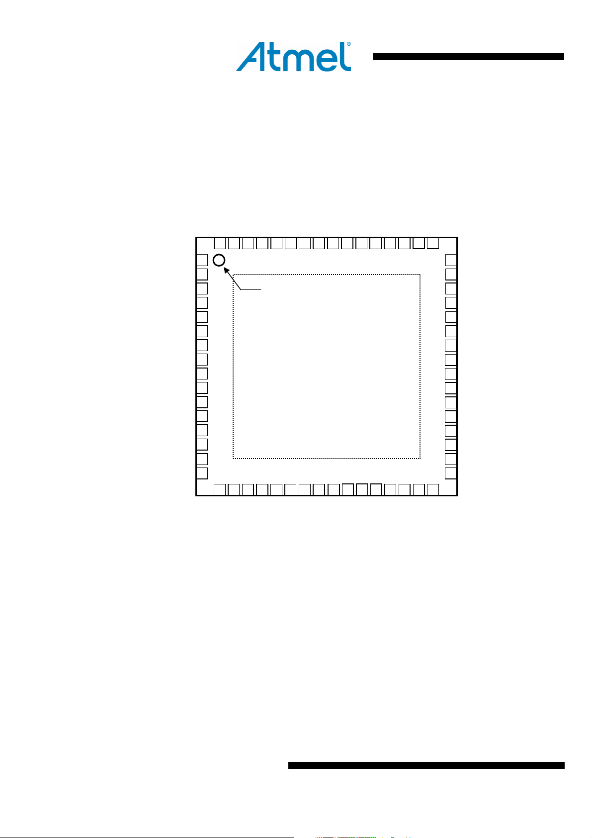
1 Pin Configurations
The large center pad underneath the QFN/MLF package is made of metal and internally connected
to AVSS. It should be soldered or glued to the board to ensure good mechanical stability. If the
nnected, the package might loosen from the board. It is not recommended to
62 61 60 59 58 57 64 63
17 18 19 20 21 23 22 24 25 26
[PD3:TXD1:INT3]
[PD2:RXD1:INT2]
[PD1:SDA:INT1]
[PD0:SCL:INT0]
[DVSS]
[DVDD] [DVDD]
[DVSS:DSVSS]
[PG5:OC0B]
[PG4:TOSC1] [PG3:TOSC2]
[PD6:T1]
[PG1:DIG1]
[PD5:XCK1]
[PD4:ICP1]
Figure 1-1. Pinout ATmega256/128/64RFR2
[PF2:ADC2:DIG2]
[PF3:ADC3:DIG4]
[PF4:ADC4:TCK]
[PF5:ADC5:TMS]
[PF6:ADC6:TDO]
[PF7:ADC7:TDI]
[AVSS_RFP]
[RFP]
[RFN]
[AVSS_RFN]
[TST]
[RSTN]
[RSTON]
[PG0:DIG3]
[PG2:AMR]
10
11
12
13
14
15
16
1
2
3
4
5
6
7
8
9
Index corner
56 55 54 53 52 51
ATmega256/128/64RFR2
Exposed paddle: [AVSS]
27
28
29
C3C:INT5]
50 49
[PE2:XCK0:AIN0]
48
[PE1:TXD0]
47
[PE0:RXD0:PCINT8]
46
[DVSS]
45
[DEVDD]
44
[PB7:OC0A:OC1C:PCINT7]
43
[PB6:OC1B:PCINT6]
42
[PB5:OC1A:PCINT5]
41
[PB4:OC2A:PCINT4]
40
[PB3:MISO:PDO:PCINT3]
39
[PB2:MOSI:PDI:PCINT2]
38
[PB1:SCK:PCINT1]
37
[PB0:SSN:PCINT0]
36
[DVSS]
35
[DEVDD]
34
[CLKI]
33
31 32
30
2 Disclaimer
2
[DEVDD]
Note:
center pad is left unco
use the exposed paddle as a replacement of the regular AVSS pins.
Typical values contained in this datasheet are based on simulation and characterization
results of other AVR microcontrollers and radio transceivers manufactured in a similar
process technology. Minimum and Maximum values will be available after the device is
characterized.
[PD7:T0]
8393CS-MCU Wireless-09/14
Page 3
3
ATmega256/128/64RFR2
3 Overview
The ATmega256/128/64RFR2 is a low-power CMOS 8-bit microcontroller based on the
AVR enhanced RISC architecture combined with a high data rate transceiver for the 2.4
GHz ISM band.
By executing powerful instructions in a single clock cycle, the device achieves
throughputs approaching 1 MIPS per MHz allowing the system designer to optimize
power consumption versus processing speed.
The radio transceiver provides high data rates from 250 kb/s up to 2 Mb/s, frame
handling, outstanding receiver sensitivity and high transmit output power enabling a
very robust wireless communication.
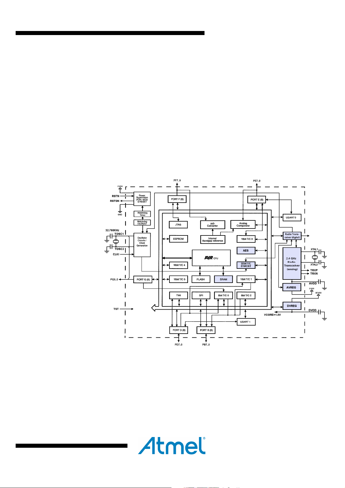
3.1 Block Diagram
Figure 3-1 Block Diagram
The AVR core combines a rich instruction set with 32 general purpose working
registers. All 32 registers are directly connected to the Arithmetic Logic Unit (ALU). Two
independent registers can be accessed with one single instruction executed in one
clock cycle. The resulting architecture is very code efficient while achieving throughputs
up to ten times faster than conventional CISC microcontrollers. The system includes
internal voltage regulation and an advanced power management. Distinguished by the
small leakage current it allows an extended operation time from battery.
The radio transceiver is a fully integrated ZigBee solution using a minimum number of
external components. It combines excellent RF performance with low cost, small size
and low current consumption. The radio transceiver includes a crystal stabilized
fractional-N synthesizer, transmitter and receiver, and full Direct Sequence Spread
8393CS-MCU Wireless-09/14
Page 4
ATmega256/128/64RFR2
700nA
Spectrum Signal (DSSS) processing with spreading and despreading. The device is
fully compatible with IEEE802.15.4-2011/2006/2003 and ZigBee standards.
The ATmega256/128/64RFR2 provides the following features: 256K/128K/64K Bytes of
In-System Programmable (ISP) Flash with read-while-write capabilities, 8K/4K/2K Bytes
EEPROM, 32K/16K/8K Bytes SRAM, up to 35 general purpose I/O lines, 32 general
purpose working registers, Real Time Counter (RTC), 6 flexible Timer/Counters with
compare modes and PWM, a 32 bit Timer/Counter, 2 USART, a byte oriented 2-wire
Serial Interface, a 8 channel, 10 bit analog to digital converter (ADC) with an optional
differential input stage with programmable gain, programmable Watchdog Timer with
Internal Oscillator, a SPI serial port, IEEE std. 1149.1 compliant JTAG test interface,
also used for accessing the On-chip Debug system and programming and 6 software
selectable power saving modes.
The Idle mode stops the CPU while allowing the SRAM, Timer/Counters, SPI port, and
interrupt system to continue functioning. The Power-down mode saves the register
contents but freezes the Oscillator, disabling all other chip functions until the next
interrupt or hardware reset. In Power-save mode, the asynchronous timer continues to
run, allowing the user to maintain a timer base while the rest of the device is sleeping.
The ADC Noise Reduction mode stops the CPU and all I/O modules except
asynchronous timer and ADC, to minimize switching noise during ADC conversions. In
Standby mode, the RC oscillator is running while the rest of the device is sleeping. This
allows very fast start-up combined with low power consumption. In Extended Standby
mode, both the main RC oscillator and the asynchronous timer continue to run.
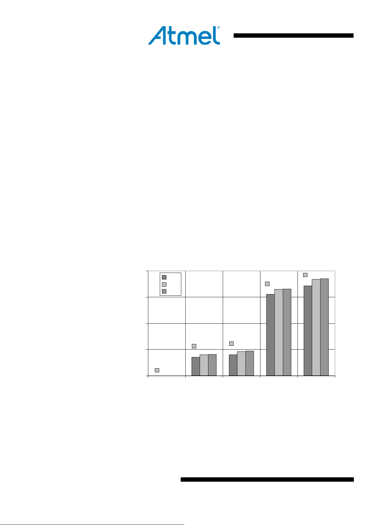
Typical supply current of the microcontroller with CPU clock set to 16MHz and the radio
transceiver for the most important states is shown in the
Figure 3-2 below.
Figure 3-2 Radio transceiver and microcontroller (16MHz) supply current
20
15
10
5
I(DEVDD,EVDD) [mA]
0
The transmit output power is set to maximum. If the radio transceiver is in SLEEP mode
the current is dissipated by the AVR microcontroller only.
In Deep Sleep mode all major digital blocks with no data retention requirements are
disconnected from main supply providing a very small leakage current. Watchdog timer,
MAC symbol counter and 32.768kHz oscillator can be configured to continue to run.
250nA
Deep Sleep SLEEP TRX_OFF RX_ON BUSY_TX
Radio transceiver and microcontroller (16MHz) supply current
1.8V
3.0V
3.6V
4,1mA
RPC disabled
RPC enabled □ 10.1mA
4,7mA
16,6mA
18,6mA
4
8393CS-MCU Wireless-09/14
Page 5

5
ATmega256/128/64RFR2
The device is manufactured using Atmel’s high-density nonvolatile memory technology.
The On-chip ISP Flash allows the program memory to be reprogrammed in-system
trough an SPI serial interface, by a conventional nonvolatile memory programmer, or by
on on-chip boot program running on the AVR core. The boot program can use any
interface to download the application program in the application Flash memory.
Software in the boot Flash section will continue to run while the application Flash
section is updated, providing true Read-While-Write operation. By combining an 8 bit
RISC CPU with In-System Self-Programmable Flash on a monolithic chip, the Atmel
ATmega256/128/64RFR2 is a powerful microcontroller that provides a highly flexible
and cost effective solution to many embedded control applications.
The ATmega256/128/64RFR2 AVR is supported with a full suite of program and system
development tools including: C compiler, macro assemblers, program
debugger/simulators, in-circuit emulators, and evaluation kits.
3.2 Pin Descriptions
3.2.1 EVDD
3.2.2 DEVDD
3.2.3 AVDD
3.2.4 DVDD
3.2.5 DVSS
3.2.6 AVSS
3.2.7 Port B (PB7...PB0)
External analog supply voltage.
External digital supply voltage.
Regulated analog supply voltage (internally generated).
Regulated digital supply voltage (internally generated).
Digital ground.
Analog ground.
Port B is an 8-bit bi-directional I/O port with internal pull-up resistors (selected for each
bit). The Port B output buffers have symmetrical drive characteristics with both high sink
and source capability. As inputs, Port B pins that are externally pulled low will source
current if the pull-up resistors are activated. The Port B pins are tri-stated when a reset
condition becomes active, even if the clock is not running.
Port B also provides functions of various special features of the
ATmega256/128/64RFR2.
3.2.8 Port D (PD7...PD0)
Port D is an 8-bit bi-directional I/O port with internal pull-up resistors (selected for each
bit). The Port D output buffers have symmetrical drive characteristics with both high sink
and source capability. As inputs, Port D pins that are externally pulled low will source
current if the pull-up resistors are activated. The Port D pins are tri-stated when a reset
condition becomes active, even if the clock is not running.
Port D also provides functions of various special features of the
ATmega256/128/64RFR2.
3.2.9 Port E (PE7...PE0)
Port E is an 8-bit bi-directional I/O port with internal pull-up resistors (selected for each
bit). The Port E output buffers have symmetrical drive characteristics with both high sink
and source capability. As inputs, Port E pins that are externally pulled low will source
8393CS-MCU Wireless-09/14
Page 6

ATmega256/128/64RFR2
3.2.10 Port F (PF7...PF0)
current if the pull-up resistors are activated. The Port E pins are tri-stated when a reset
condition becomes active, even if the clock is not running.
Port E also provides functions of various special features of the
ATmega256/128/64RFR2.
Port F is an 8-bit bi-directional I/O port with internal pull-up resistors (selected for each
bit). The Port F output buffers have symmetrical drive characteristics with both high sink
and source capability. As inputs, Port F pins that are externally pulled low will source
current if the pull-up resistors are activated. The Port F pins are tri-stated when a reset
condition becomes active, even if the clock is not running.
Port F also provides functions of various special features of the
ATmega256/128/64RFR2.
3.2.11 Port G (PG5…PG0)
3.2.12 AVSS_RFP
3.2.13 AVSS_RFN
3.2.14 RFP
3.2.15 RFN
3.2.16 RSTN
Port G is a 6-bit bi-directional I/O port with internal pull-up resistors (selected for each
bit). The Port G output buffers have symmetrical drive characteristics with both high
sink and source capability. However the driver strength of PG3 and PG4 is reduced
compared to the other port pins. The output voltage drop (VOH, VOL) is higher while the
leakage current is smaller. As inputs, Port G pins that are externally pulled low will
source current if the pull-up resistors are activated. The Port G pins are tri-stated when
a reset condition becomes active, even if the clock is not running.
Port G also provides functions of various special features of the
ATmega256/128/64RFR2.
AVSS_RFP is a dedicated ground pin for the bi-directional, differential RF I/O port.
AVSS_RFN is a dedicated ground pin for the bi-directional, differential RF I/O port.
RFP is the positive terminal for the bi-directional, differential RF I/O port.
RFN is the negative terminal for the bi-directional, differential RF I/O port.
Reset input. A low level on this pin for longer than the minimum pulse length will
generate a reset, even if the clock is not running. Shorter pulses are not guaranteed to
generate a reset.
3.2.17 RSTON
Reset output. A low level on this pin indicates a reset initiated by the internal reset
sources or the pin RSTN.
3.2.18 XTAL1
Input to the inverting 16MHz crystal oscillator amplifier. In general a crystal between
XTAL1 and XTAL2 provides the 16MHz reference clock of the radio transceiver.
3.2.19 XTAL2
Output of the inverting 16MHz crystal oscillator amplifier.
3.2.20 AREF
Reference voltage output of the A/D Converter. In general this pin is left open.
3.2.21 TST
Programming and test mode enable pin. If pin TST is not used pull it to low.
6
8393CS-MCU Wireless-09/14
Page 7
7
ATmega256/128/64RFR2
3.2.22 CLKI
3.3 Unused Pins
Input to the clock system. If selected, it provides the operating clock of the
microcontroller.
Floating pins can cause power dissipation in the digital input stage. They should be
connected to an appropriate source. In normal operation modes the internal pull-up
resistors can be enabled (in Reset all GPIO are configured as input and the pull-up
resistors are still not enabled).
Bi-directional I/O pins shall not be connected to ground or power supply directly.
The digital input pins TST and CLKI must be connected. If unused pin TST can be
connected to AVSS while CLKI should be connected to DVSS.
Output pins are driven by the device and do not float. Power supply pins respective
ground supply pins are connected together internally.
XTAL1 and XTAL2 shall never be forced to supply voltage at the same time.
3.4 Configuration summary
According to the application requirements a variable memory size allows to optimize
current consumption and leakage current.
Table 3-1 Memory Configuration
Package and associated pin configuration are the same for all devices providing full
functionality to the application.
Table 3-2 System Configuration
Device Flash EEPROM SRAM
ATmega256RFR2 256KB 8KB 32KB
ATmega128RFR2 128KB 4KB 16KB
ATmega64RFR2 64KB 2KB 8KB
Device Package GPIO Serial IF ADC channel
ATmega256RFR2 QFN 38 2 USART, SPI, TWI 8
ATmega128RFR2 QFN 38 2 USART, SPI, TWI 8
ATmega64RFR2 QFN 38 2 USART, SPI, TWI 8
The devices are optimized for applications based on the ZigBee and the IEEE 802.15.4
specification. Having application stack, network layer, sensor interface and an excellent
power control combined in a single chip many years of operation should be possible.
Table 3-3 Application Profile
Device Application
ATmega256RFR2 Large Network Coordinator / Router for IEEE 802.15.4 / ZigBee Pro
ATmega128RFR2 Network Coordinator / Router for IEEE 802.15.4
ATmega64RFR2 End node device / network processor
8393CS-MCU Wireless-09/14
Page 8

ATmega256/128/64RFR2
3.5 Compatibility to ATmega1281/2561
The basic AVR feature set of the ATmega256/128/64RFR2 is derived from the
ATmega1281/2561. Address locations and names of the implemented modules and
registers are unchanged as long as it fits the target application of a very small and
power efficient radio system. In addition, several new features were added.
Backward compatibility of the ATmega256/128/64RFR2 to the ATmega1281/2561 is
provided in most cases. However some incompatibilities between the microcontrollers
exist.
3.5.1 Port A and Port C
Port A and Port C are not implemented. The associated registers are available but will
not provide any port control. Remaining ports are kept at their original address location
to not require changes of existing software packages.
3.5.2 External Memory Interface
The alternate pin function “External Memory interface” using Port A and Port C is not
implemented due to the missing ports.
The large internal data memory (SRAM) does not require an external memory and the
associated parallel interface. It keeps the system radiation (EMC) at a very small level
to provide very high sensitivity at the antenna input.
3.5.3 High Voltage Programming Mode
Alternate pin function BS2 (high voltage programming) of pin PA0 is mapped to a
different pin. Entering the parallel programming mode is controlled by the TST pin.
3.5.4 AVR Oscillators and External Clock
The AVR microcontroller can utilize the high performance crystal oscillator of the
2.4GHz transceiver connected to the pins XTAL1 and XTAL2. An external clock can be
applied to the microcontroller using the clock input CLKI.
3.5.5 Analog Frontend
The ATmega256/128/64RFR2 has a new A/D converter. Software compatibility is
basically assured. Nevertheless to benefit from the higher conversion speeds and the
better performance some changes are required.
8
8393CS-MCU Wireless-09/14
Page 9
9
ATmega256/128/64RFR2
4 Application Circuits
4.1 Basic Application Schematic
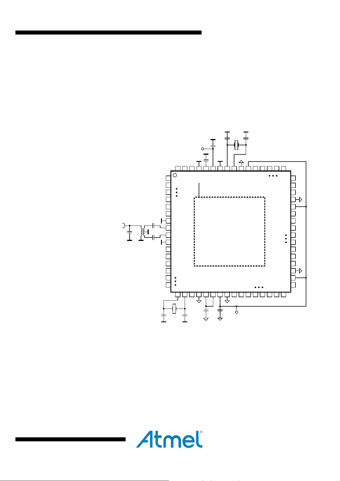
A basic application schematic of the ATmega256/128/64RFR2 with a single-ended RF
connector is shown in Figure 4-1 below and the associated Bill of Material in Table 4-1
on page 10. The 50Ω single-ended RF input is transformed to the 100Ω differential RF
port impedance using Balun B1. The capacitors C1 and C2 provide AC coupling of the
RF input to the RF port, capacitor C4 improves matching.
Figure 4-1. Basic Application schematic (64-pin package)
RF
B1
C4
Pins TST & CLKI
must be connected
CX1 CX2
CB2
V
64
1
2
3
4
5
6
PF7
AVSS
C1
C2
7
8
RFP
RFN
9
AVSS
10
TST
11
RSTN
12
RSTON
13
PG0
14
15
16
17 18 19 20 21 22 23 24
DD
CB1
PF0
AREF
AVSS
AVDD
EVDD
DVSS
DVDD
PG5
DVDD
XTAL
5455 4950515253
5657585960616263
AVSS
XTAL2
XTAL1
DEVDD
DVSS
PD0
25 26 27 28 29 30 31 32
PE7
DVSS
DEVDD
PE0
DVSS
DEVDD
PB7
PB0
DVSS
DEVDD
48
47
46
45
44
43
42
41
40
39
38
37
36
35
34
CLKI
33
PD7
8393CS-MCU Wireless-09/14
V
CB4
XTAL
CX3 CX4
32kHz
The power supply bypass capacitors (CB2, CB4) are connected to the external analog
supply pin (EVDD, pin 59) and external digital supply pin (DEVDD, pin 23). Pins 34, 44
and 54 supply the digital port pins.
Floating pins can cause excessive power dissipation (e.g. during power on). They
should be connected to an appropriate source. GPIO shall not be connected to ground
or power supply directly.
The digital input pins TST and CLKI must be connected. If pin TST will never be used it
can be connected to AVSS while an unused pin CLKI could be connected to DVSS (see
chapter "Unused Pins" on page 7).
Capacitors CB1 and CB3 are bypass capacitors for the integrated analog and digital
voltage regulators to ensure stable operation and to improve noise immunity.
CB3
DD
Page 10

ATmega256/128/64RFR2
Capacitors should be placed as close as possible to the pins and should have a lowresistance and low-inductance connection to ground to achieve the best performance.
The crystal (XTAL), the two load capacitors (CX1, CX2), and the internal circuitry
connected to pins XTAL1 and XTAL2 form the 16MHz crystal oscillator for the 2.4GHz
transceiver. To achieve the best accuracy and stability of the reference frequency, large
parasitic capacitances must be avoided. Crystal lines should be routed as short as
possible and not in proximity of digital I/O signals. This is especially required for the
High Data Rate Modes.
The 32.768 kHz crystal connected to the internal low power (sub 1µA) crystal oscillator
provides a stable time reference for all low power modes including 32 Bit IEEE 802.15.4
Symbol Counter (
asynchronous timer T/C2 ("Timer/Counter2 with PWM and Asynchronous Operation").
Total shunt capacitance including CX3, CX4 should not exceed 15pF across both pins.
The very low supply current of the oscillator requires careful layout of the PCB and any
leakage path must be avoided.
Crosstalk and radiation from switching digital signals to the crystal pins or the RF pins
can degrade the system performance. The programming of minimum drive strength
settings for the digital output signal is recommended (see "DPDS0 - Port Driver
Strength Register 0").
Table 4-1. Bill of Materials (BoM)
Designator Description Value Manufacturer Part Number Comment
B1 SMD balun
SMD balun / filter
CB1
CB3
CB2
CB4
CX1, CX2 16MHz crystal load
CX3, CX4 32.768kHz crystal load
C1, C2
C4 (optional) RF matching 0.47 pF Johnstech
XTAL Crystal CX-4025 16 MHz
XTAL 32kHz Crystal Rs=100 kOhm
LDO VREG
bypass capacitor
Power supply bypass
capacitor
capacitor
capacitor
RF coupling capacitor
2.4 GHz Wuerth
(100nF minimum)
(100nF minimum)
12 pF
12 … 25 pF
22 pF
SX-4025 16 MHz
"MAC Symbol Counter") and real time clock application using the
1 µF
1 µF
Johanson
Technology
AVX
Murata
AVX
Murata
Epcos
Epcos
AVX
ACAL Taitjen
Siward
748421245
2450FB15L0001
0603YD105KAT2A
GRM188R61C105KA12D
06035A120JA
GRP1886C1H120JA01
B37930
B37920
06035A220JAT2A
XWBBPL-F-1
A207-011
Filter included
X5R
(0603)
COG
(0603)
C0G 5% 50V
(0402 or 0603)
10% 16V
5% 50V
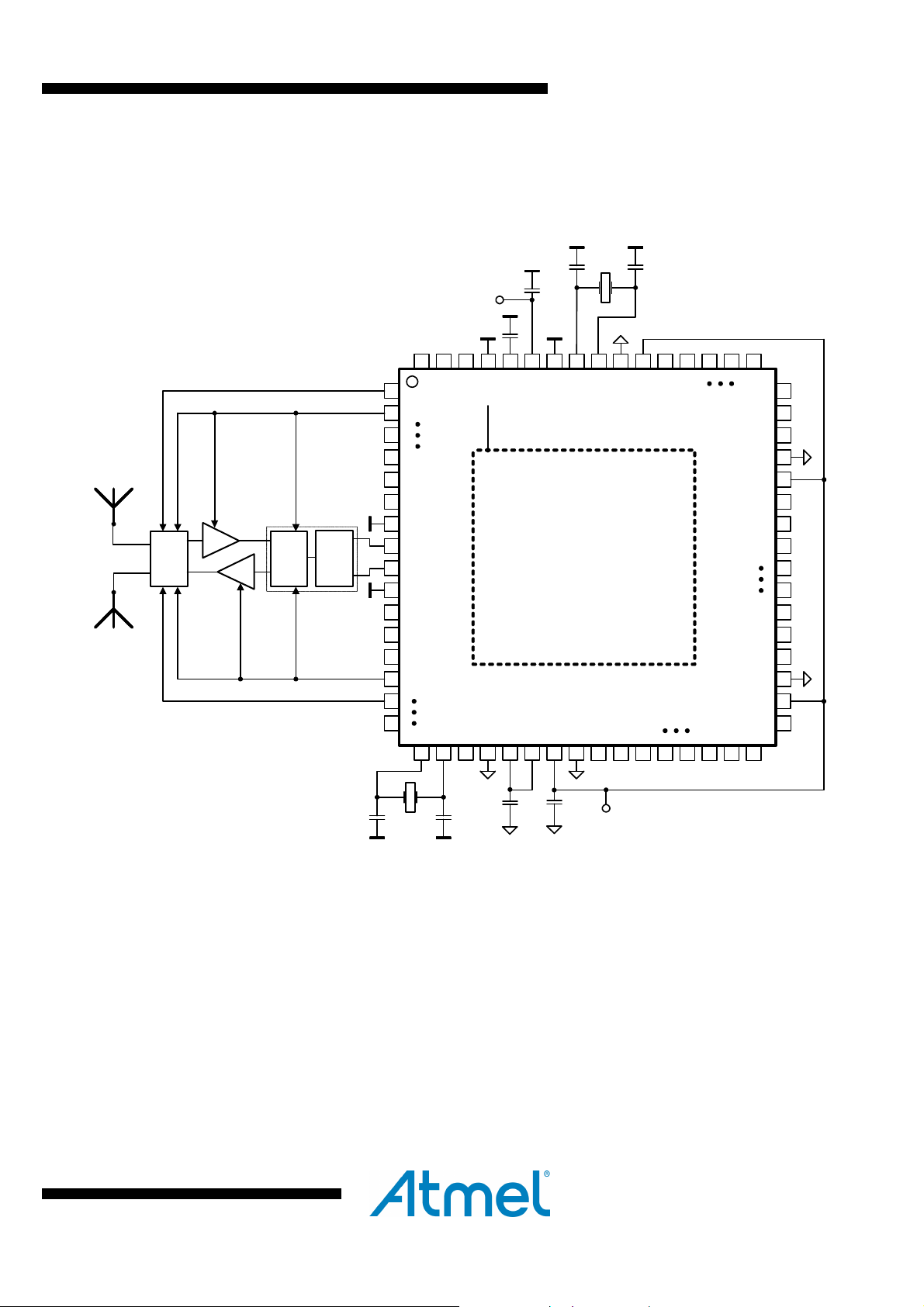
4.2 Extended Feature Set Application Schematic
The ATmega256/128/64RFR2 supports additional features like:
• Security Module (AES)
• High Data Rate Mode up to 2MBits/s
• Antenna Diversity using alternate pin function DIG1/2 at Port G and F
10
8393CS-MCU Wireless-09/14
Page 11
11
ATmega256/128/64RFR2
• RX/TX Indicator using alternate pin function DIG3/4 at Port G and F
An extended feature set application schematic illustrating the use of the
ATmega256/128/64RFR2 Extended Feature Set, is shown in Figure 4-2 below.
Figure 4-2. Extended Feature Application schematic
CX1 CX2
XTAL
CB2
V
DD
CB1
5455 4950515253
64
5657585960616263
ANT0
ANT1
SW2
1
2
3
4
5
6
N2
LNA
RF-
Switch
PA
N1
Pins TST & CLKI
must be connected
RF-
Balun
Switch
B1SW1
7
8
9
10
11
12
13
14
15
16
CX3 CX4
XTAL
32kHz
PF0
AREF
AVSS
AVDD
EVDD
PF7
AVSS
RFP
RFN
AVSS
TST
RSTN
RSTON
PG0
17 18 19 20 21 22 23 24
PG5
DVSS
DVDD
DVDD
CB3
AVSS
XTAL2
XTAL1
DEVDD
DVSS
PD0
25 26 27 28 29 30 31 32
CB4
V
PE7
DVSS
DEVDD
DD
PE0
DVSS
DEVDD
PB7
PB0
DVSS
DEVDD
PD7
48
47
46
45
44
43
42
41
40
39
38
37
36
35
34
CLKI
33
Although this example shows all additional hardware features combined, it is possible to
use all features separately or in various combinations.
8393CS-MCU Wireless-09/14
Page 12

ATmega256/128/64RFR2
5 Revision history
Please note that the referring page numbers in this section are referring to this
document. The referring revision in this section are referring to the document revision
Rev. 8393CS-MCU Wireless-09/14
1. Content unchanged - recreated for combined release with the datasheet.
Rev. 8393BS-MCU Wireless-02/13
1. Phase measurement support added to page 1.
Rev. 8393AS-MCU Wireless-11/12
1. Initial release
12
8393CS-MCU Wireless-09/14
Page 13

13
ATmega256/128/64RFR2
Table of Contents
Features .................................................................................................. 1
Applications ........................................................................................... 1
1 Pin Configurations .............................................................................. 2
2 Disclaimer ............................................................................................ 2
3 Overview .............................................................................................. 3
3.1 Block Diagram ........................................................................................................ 3
3.2 Pin Descriptions...................................................................................................... 5
3.3 Unused Pins ........................................................................................................... 7
3.4 Configuration summary .......................................................................................... 7
3.5 Compatibility to ATmega1281/2561 ....................................................................... 8
4 Application Circuits ............................................................................ 9
4.1 Basic Application Schematic .................................................................................. 9
4.2 Extended Feature Set Application Schematic ...................................................... 10
5 Revision history ................................................................................ 12
Table of Contents ................................................................................. 13
8393CS-MCU Wireless-09/14
Page 14

ATmega256/128/64RFR2
Atmel Corporation
Atmel Asia Limited
Atmel Munich GmbH
Atmel Japan G.K.
1600 Technology Drive
San Jose, CA 95110
USA
Tel: (+1)(408) 441-0311
Fax: (+1)(408) 487-2600
www.atmel.com
© 2014 Atmel Corporation. All rights reserved. / Rev.: 8393CS-MCU Wireless-09/14
Atmel®, Atmel logo and combinations thereof, Enabling Unlimited Possibilities®, and others are registered trademarks or trademarks of Atmel Corporation or its
subsidiaries. Other terms and product names may be trademarks of others.
Disclaimer: The information in this document is provided in connection with Atmel products. No license, express or implied, by estoppel or otherwise, to any intellectual property right is granted by this
document or in connection with the sale of Atmel products. EXCEPT AS SET FORTH IN THE ATMEL TERMS AND CONDITIONS OF SALES LOCATED ON THE ATMEL WEBSITE, ATMEL ASSUMES
NO LIABILITY WHATSOEVER AND DISCLAIMS ANY EXPRESS, IMPLIED OR STATUTORY WARRANTY RELATING TO ITS PRODUCTS INCLUDING, BUT NOT LIMITED TO, THE IMPLIED
WARRANTY OF MERCHANTABILITY, FITNESS FOR A PARTICULAR PURPOSE, OR NON-INFRINGEMENT. IN NO EVENT SHALL ATMEL BE LIABLE FOR ANY DIRECT, INDIRECT,
CONSEQUENTIAL, PUNITIVE, SPECIAL OR INCIDENTAL DAMAGES (INCLUDING, WITHOUT LIMITATION, DAMAGES FOR LOSS AND PROFITS, BUSINESS INTERRUPTION, OR LOSS OF
INFORMATION) ARISING OUT OF THE USE OR INABILITY TO USE THIS DOCUMENT, EVEN IF ATMEL HAS BEEN ADVISED OF THE POSSIBILITY OF SUCH DAMAGES. Atmel makes no
representations or warranties with respect to the accuracy or completeness of the contents of this document and reserves the right to make changes to specifications and products descriptions at any time
without notice. Atmel does not make any commitment to update the information contained herein. Unless specifically provided otherwise, Atmel products are not suitable for, and shall not be used in,
14
automotive applications. Atmel products are not intended, authorized, or warranted for use as components in applications intended to support or sustain life.
Unit 01-5 & 16, 19F
BEA Tower, Millennium City 5
418 Kwun Tong Road
Kwun Tong, Kowloon
HONG KONG
Tel: (+852) 2245-6100
Fax: (+852) 2722-1369
Business Campus
Parkring 4
D-85748 Garching b. Munich
GERMANY
Tel: (+49) 89-31970-0
Fax: (+49) 89-3194621
16F Shin-Osaki Kangyo Bldg.
1-6-4 Osaki, Shinagawa-ku
Tokyo 141-0032
JAPAN
Tel: (+81)(3) 6417-0300
Fax: (+81)(3) 6417-0370
8393CS-MCU Wireless-09/14
 Loading...