

Page 1

ATF15xx-DK3 Development Kit
..............................................................................................
User Guide
Page 2

Table of Contents
Section 1
Introduction ...........................................................................................1-1
1.1 CPLD Development/ Programmer Kit .......................................................1-1
1.2 Kit Contents ..............................................................................................1-1
1.3 Kit Features...............................................................................................1-1
1.3.1 CPLD Development/Programmer Board ............................................1-1
1.3.2 Logic Doubling CPLDs .......................................................................1-2
1.3.3 CPLD ISP Download Cable ................................................................1-2
1.3.4 PLD Software CD-ROM......................................................................1-2
1.4 Device Support .........................................................................................1-2
1.5 System Requirements...............................................................................1-3
1.6 Ordering Information .................................................................................1-3
1.7 References................................................................................................1-4
1.7.1 ProChip Designer ...............................................................................1-4
1.7.2 Atmel-WinCUPL .................................................................................1-4
1.7.3 ATMISP ..............................................................................................1-4
1.7.4 POF2JED ...........................................................................................1-4
1.8 Technical Support .....................................................................................1-4
Section 2
Hardware Description ...........................................................................2-1
2.1 Atmel CPLD Development/ Programmer Board........................................2-1
2.1.1 7-segment Displays with Selectable Jumpers ....................................2-2
2.1.2 LEDs with Selectable Jumpers ...........................................................2-5
2.1.3 Push-button Switches with Selectable Jumpers for I/O Pins ..............2-6
2.1.4 Push-button Switches with Selectable Jumpers for GCLR
and OE1 Pins .....................................................................................2-8
2.1.5 2 MHz Oscillator and Clock Selection Jumper ...................................2-9
2.1.6 VCCIO and VCCINT Voltage Selection Jumpers and LEDs ............2-10
2.1.7 ICCIO and ICCINT Jumpers .............................................................2-10
2.1.8 Voltage Regulators ...........................................................................2-10
2.1.9 Power Supply Switch and Power LED..............................................2-10
2.1.10 Power Supply Jack and Power Supply Header ................................2-10
2.1.11 JTAG ISP Connector and TDO Selection Jumper............................2-11
2.2 Socket Adapter Board .............................................................................2-12
2.3 Atmel CPLD ISP Download Cable ..........................................................2-13
ATF15xx-DK3 Development Kit User Guide i
3605B–PLD–05/06
Page 3

Table of Contents
Section 3
CPLD Design Flow Tutorial ..................................................................3-1
3.1 Create a Project using the “New Project Wizard” .....................................3-1
3.2 Add a Design File......................................................................................3-7
3.3 Synthesize the VHDL Design....................................................................3-7
3.4 Fit the Synthesized Design File ................................................................3-8
3.5 Program and Verify Design .....................................................................3-10
Section 4
Schematic Diagrams and VHDL File .................................................... 4-1
ii ATF15xx-DK3 Development Kit User Guide
3605B–PLD–05/06
Page 4

Section 1
Introduction
1.1 CPLD
Development/
Programmer Kit
The Atmel CPLD Development/Programmer Kit (P/N: ATF15xx-DK3) is a complete
development system and an In-System Programming (ISP) programmer for the
ATF15xx family of industry standard pin compatible Complex Programmable Logic
Devices (CPLDs) with Logic Doubling
and easy way to develop prototypes and evaluate new designs with an ATF15xx ISP
CPLD. The ATF15xx family of ISP CPLDs includes the ATF15xxAS, ATF15xxASL,
ATF15xxASV, ATF15xxASVL, and ATF15xxBE CPLDs. With the availability of the different Socket Adapter Boards to support all the package types
family of ISP CPLDs, this CPLD Development/Programmer Board can be used as an
ISP programmer to program the ATF15xx ISP CPLDs in all the available package
(1)
types
through the industry standard JTAG interface (IEEE 1149.1).
®
features. This kit provides designers a very quick
1.2 Kit Contents CPLD Development/Programmer Board
44-pin TQFP Socket Adapter Board (P/N: ATF15xx-DK3-SAA44)
Atmel CPLD ISP Multi-Volt (MV) Download Cable
Atmel PLD Software CDs (includes ProChip Designer
ModelSim, latest ProChip patch, Atmel-WinCUPL™, and other EPLD software)
Two 44-pin TQFP Sample Devices (one ATF1502BE and one ATF1504ASV)
Notes: 1. Socket adapter board for 100-pin PQFP is not offered.
2. Only the 44-pin TQFP Socket Adapter Board is included in this kit. Other Socket
Adapter Boards are sold separately. Please refer to Section 1.6 for ordering information of the Socket Adapter Boards.
(1)
offered in the ATF15xx
(2)
®
, Precision RTL Synthesis,
1.3 Kit Features
1.3.1 CPLD Development/
Programmer Board
ATF15xx-DK3 Development Kit User Guide 1-1
10-pin JTAG-ISP port
Regulated power supply circuits for 9V DC power source
Selectable 5V, 3.3V, 2.5V, or 1.8V I/O voltage supply
Selectable 1.8V, 3.3V, or 5.0V core voltage supply
3605B–PLD–05/06
Page 5

Introduction
44-pin TQFP Socket Adapter Board
Headers for I/O pins of the ATF15xx device
2 MHz Crystal Oscillator
Four 7-segment LED displays
Eight individual LEDs
Eight push-button switches
Global Clear and Output Enable push-button switches
Current measurement jumpers
1.3.2 Logic Doubling
CPLDs
1.3.3 CPLD ISP Download
ATF1502BE 1.8V low-power 32-macrocell ISP CPLD with Logic Doubling architecture
ATF1504ASV 3.3V 64-macrocell ISP CPLD with Logic Doubling architecture
5V/3.3V/2.5V/1.8V ISP Download Cable for PC Parallel Printer (LPT) Port
Cable
1.3.4 PLD Software CDROM
Free Atmel-WinCUPL Design Software
ProChip Designer v4.0
ProChip Designer v4.0 Patch
Precision RTL Synthesis
ModelSim
Atmel CPLD ISP Software (ATMISP)
POF2JED Conversion Utility
User Guides and Tutorials
1.4 Device Support The Atmel CPLD Development/Programmer Board supports the following devices in all
speed grades and packages (except 100-PQFP):
ATF1502BE ATF1508ASV/ASVL
ATF1502AS/ASL ATF1502ASV
ATF1504BE ATF1504ASV/ASVL
ATF1504AS/ASL ATF1508AS/ASL
1-2 ATF15xx-DK3 Development Kit User Guide
3605B–PLD–05/06
Page 6

Introduction
1.5 System
Requirements
1.6 Ordering
Information
The minimum hardware and software requirements to program an ATF15xx ISP CPLD
designed using the ProChip Designer Software on the CPLD Development/Programmer
Board through the Atmel CPLD ISP Software (ATMISP) V6.0 or later are:
Pentium
Windows XP
®
or Pentium-compatible microprocessor-based computer
®
, Windows® 98, Windows NT® 4.0, or Windows 2000
64-MByte RAM
200-MByte free hard disk space
Windows-supported mouse
Available parallel printer (LPT) port
9V DC power supply with 500 mA of supply current
SVGA monitor (800 x 600 resolution)
Part Number Description
ATF15xx-DK3 Atmel CPLD Development/Programmer Kit
(includes ATF15xxDK3-SAA44)
ATF15xxDK3-SAA100 100-pin TQFP Socket Adapter Board for DK3 Board
ATF15xxDK3-SAJ44 44-pin PLCC Socket Adapter Board for DK3 Board
ATF15xxDK3-SAJ84 84-pin PLCC Socket Adapter Board for DK3 Board
ATF15xxDK3-SAA44 44-pin TQFP Socket Adapter Board for DK3 Board
Other socket adapters to support other packages will be available in the near future.
ATF15xx-DK3 Development Kit User Guide 1-3
3605B–PLD–05/06
Page 7
Introduction
1.7 References To help PLD designers use the different Atmel PLD software, documentation such as
help files, tutorials, application notes/briefs, and user guides are available.
1.7.1 ProChip Designer
ProChip Desinger
Help Files
Tutorials From the ProChip Designer main window, click on HELP and then
Known Problems &
Solutions
1.7.2 Atmel-WinCUPL
Help Files From the Atmel-WinCUPL main window, click on HELP and then
CUPL Programmers
Reference Guide
Tutorials From the Atmel-WinCUPL main window, click on HELP, select ATMEL
From the ProChip Designer main window, click on HELP and then
select PROCHIP DESIGNER HELP.
select TUTORIALS.
From the ProChip Designer main window, click on HELP and then
select REVIEW KPS.
select CONTENTS.
From the Atmel-WinCUPL main window, click on HELP and then
select CUPL PROGRAMMERS REFERENCE.
INFO and then select TUTORIAL1.PDF.
1.7.3 ATMISP
1.7.4 POF2JED
1.8 Technical
Support
Known Problems &
Solutions
Help Files From the ATMISP main window, click on HELP and then select ISP
Tutorials From the ATMISP main window, click on HELP, and then select
Known Problems &
Solutions
ATF15xx Conversion
Application Brief
From the Atmel-WinCUPL main window, click on HELP, select ATMEL
INFO and then select CUPL_BUG.PDF.
HELP.
ATMISP TUTORIAL.
Using Windows Explorer, go to the directory where ATMISP is
installed and open the README.TXT file through any ASCII text
editor.
from the POF2JED main window, click on HELP and then select
CONVERSION OPTIONS.
For technical support on any Atmel PLD related issues, please contact Atmel PLD Applications Group at:
URL: www.atmel.com/dyn/products/support.asp
FAQ: www.atmel.com/dyn/products/tech_support.asp?faq=y
Hotline: 1-408-436-4333
Email : pld@atmel.com
1-4 ATF15xx-DK3 Development Kit User Guide
3605B–PLD–05/06
Page 8
Section 2
Hardware Description
2.1 Atmel CPLD
Development/
Programmer
Board
Atmel CPLD Development/Programmer Board along with the Socket Adapter Board as
shown in Figure 2-1 contains many features that designers will find very useful when
developing, prototyping, or evaluating their ATF15xx CPLD design. Features such as
push-button switches, LEDs, 7-segment displays, 2-MHz crystal oscillator,
5V/3.3V/2.5V/1.8V VCCI/O selector, 1.8V/3.3V/5.0V VCCINT selector, JTAG-ISP port,
and socket adapters make this a very versatile starter/development kit and an ISP programmer for the ATF15xx family of JTAG-ISP CPLDs.
Figure 2-1. CPLD Development/Programmer Board with 44-pin TQFP Socket Adapter Board
VccIO LED
VCCINT Selector
VccINT LED
Power LED
Clock Selector
Power Switch
Oscillator
Power Supply Jack
Voltage
Regulators
VccIO
Selector
GCLR
Switch
GOE
Switch
7-Segment
Displays
IccIO Jumper
IccINT Jumper
ATF15xxDK3-SAA44
Socket Adapter Board
User I/O
Pin Headers
Power Supply Header
JTAG Cascade Jumper
Device Socket
JTAG ISP Header
ATF15xx-DK3 Development Kit User Guide 2-1
LEDs
Push-Button Switches
3605B–PLD–05/06
Page 9
Hardware Description
2.1.1 7-segment Displays
with Selectable
Jumpers
Atmel CPLD Development/Programmer Board contains four seven-segment displays to
allow the designers to observe the outputs of the ATF15xx CPLD. These four displays
are labeled DSP1, DSP2, DSP3, and DSP4, and have common anode LEDs with the
common anode lines connected to VCCIO (I/O supply voltage for the CPLD) through
series resistors with selectable jumpers labeled JPDSP1, JPDSP2, JPDSP3, or
JPDSP4. These jumpers can be removed to disable the displays by unconnecting the
VCCIO to the displays. Individual cathode lines are connected to the I/O pins of the
ATF15xx CPLD on the CPLD Development/Programmer Board. To turn on a particular
segment including the DOT of a display, the corresponding ATF15xx I/O pin connected
to this LED segment must be in a logic low state with the corresponding selectable
jumper set. Hence, the outputs of the ATF15xx need to be configured as active-low outputs in the design file. These displays work best at 2.5V VCCIO or higher.
Each segment of each display is hard-wired to one specific I/O pin of the ATF15xx. For
the higher pin count devices (100-pin and larger), all seven segments and the DOT segments of the four displays are connected to the I/O pins of the ATF15xx. However, for
the lower pin count devices, only a subset of the displays (1st and 4th displays) are connected to the ATF15xx’s I/O pins. Tables 2-1, 2-2, 2-3, and 2-4 show the connections for
7-segment displays to the ATF15xx in different package types. The circuit schematic of
the displays and jumpers is shown in Figure 2-2.
Figure 2-2. Circuit Diagram of 7-segment Display and Jumpers
2-2 ATF15xx-DK3 Development Kit User Guide
3605B–PLD–05/06
Page 10
Hardware Description
Table 2-1. Connections of ATF15xx 44-pin TQFP to 7-segment Displays
DSP/Segment PLD Pin # DSP/Segment PLD Pin #
1/A 27 3/A NC
1/B 33 3/B NC
1/C 30 3/C NC
1/D 21 3/D NC
1/E 18 3/E NC
1/F 23 3/F NC
1/G 20 3/G NC
1/DOT 31 3/DOT NC
2/A NC 4/A 3
2/B NC 4/B 10
2/C NC 4/C 6
2/D NC 4/D 43
2/E NC 4/E 35
2/F NC 4/F 42
2/G NC 4/G 34
2/DOT NC 4/DOT 11
Table 2-2. Connections of ATF15xx 44-pin PLCC to 7-segment Displays
DSP/Segment PLD Pin # DSP/Segment PLD Pin #
1/A 33 3/A NC
1/B 39 3/B NC
1/C 36 3/C NC
1/D 27 3/D NC
1/E 24 3/E NC
1/F 29 3/F NC
1/G 26 3/G NC
1/DOT 37 3/DOT NC
2/A NC 4/A 9
2/B NC 4/B 16
2/C NC 4/C 12
2/D NC 4/D 5
2/E NC 4/E 41
2/F NC 4/F 4
2/G NC 4/G 40
2/DOT NC 4/DOT 17
ATF15xx-DK3 Development Kit User Guide 2-3
3605B–PLD–05/06
Page 11

Hardware Description
Table 2-3. Connections of ATF15xx 84-pin PLCC to 7-segment Displays
DSP/Segment PLD Pin # DSP/Segment PLD Pin #
1/A 68 3/A 22
1/B 74 3/B 28
1/C 70 3/C 25
1/D 63 3/D 21
1/E 58 3/E 16
1/F 65 3/F 17
1/G 61 3/G 12
1/DOT 73 3/DOT 29
2/A 52 4/A 5
2/B 57 4/B 10
2/C 55 4/C 8
2/D 48 4/D 79
2/E 41 4/E 76
2/F 50 4/F 77
2/G 45 4/G 75
2/DOT 50 4/DOT 11
Table 2-4. Connections of ATF15xx 100-pin TQFP to 7-segment Displays
DSP/Segment PLD Pin # DSP/Segment PLD Pin #
1/A 67 3/A 13
1/B 71 3/B 19
1/C 69 3/C 16
1/D 61 3/D 8
1/E 57 3/E 83
1/F 64 3/F 6
1/G 60 3/G 92
1/DOT 75 3/DOT 20
2/A 52 4/A 100
2/B 54 4/B 94
2/C 47 4/C 97
2/D 41 4/D 81
2/E 46 4/E 76
2/F 40 4/F 80
2/G 45 4/G 79
2/DOT 56 4/DOT 93
2-4 ATF15xx-DK3 Development Kit User Guide
3605B–PLD–05/06
Page 12
Hardware Description
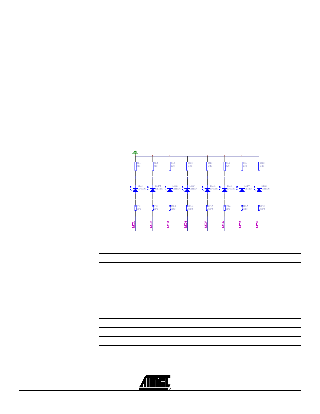
2.1.2 LEDs with
Selectable Jumpers
Atmel CPLD Development/Programmer Board has eight individual LEDs, which allow
designers to display the output signals from the user I/Os of the ATF15xx CPLD. These
eight LEDs are labeled LED1 to LED8 on the Atmel CPLD Development/Programmer
Board. The cathode of each LED is connected to ground through a series resistor while
the anode of each LED is connected to a user I/O pin of the CPLD through the
JPL1/JPL2/PL3/JPL4/JPL5/JPL6/JPL7/JPL8 selectable jumper. These jumpers can be
removed to disable the LEDs by unconnecting the anodes of the LEDs to the I/O pins of
the CPLD. Figure 2-3 shows the circuit diagram of the LEDs with the selection jumpers.
To turn on a particular LED, the corresponding ATF15xx I/O pin connected to the LED
must be in a logic high state with the corresponding jumper set. Hence, the outputs of
the ATF15xx need to be configured as active-high outputs in the design files. These
LEDs work best at 2.5V VCCIO or higher.
The lower pin-count devices (44-pin) only have four I/Os connected to LED1, LED2,
LED3, and LED4. For the higher pin-count devices (100-pin and larger), all eight LEDs
are connected to the I/Os of the device. Tables 2-5, 2-6, 2-7, and 2-8 show the connections of the CPLD I/Os to the LEDs in the different package types.
Figure 2-3. Circuit Diagram of the LEDs and Jumpers
Table 2-5. Connections of ATF15xx 44-pin TQFP to LEDs
LED # PLD Pin #
LED1 28
LED2 25
LED3 22
LED4 19
Table 2-6. Connections of ATF15xx 44-pin PLCC to LEDs
LED # PLD Pin #
LED1 34
LED2 31
LED3 28
LED4 25
ATF15xx-DK3 Development Kit User Guide 2-5
3605B–PLD–05/06
Page 13
Hardware Description
Table 2-7. Connections of ATF15xx 84-pin PLCC to LEDs
LED # PLD Pin #
LED1 69
LED2 67
LED3 64
LED4 60
LED5 27
LED6 24
LED7 18
LED8 15
Table 2-8. Connections of ATF15xx 100-pin TQFP to LEDs
LED # PLD Pin #
LED1 68
LED2 65
LED3 63
2.1.3 Push-button
Switches with
Selectable Jumpers
for I/O Pins
LED4 58
LED5 17
LED6 14
LED7 10
LED8 9
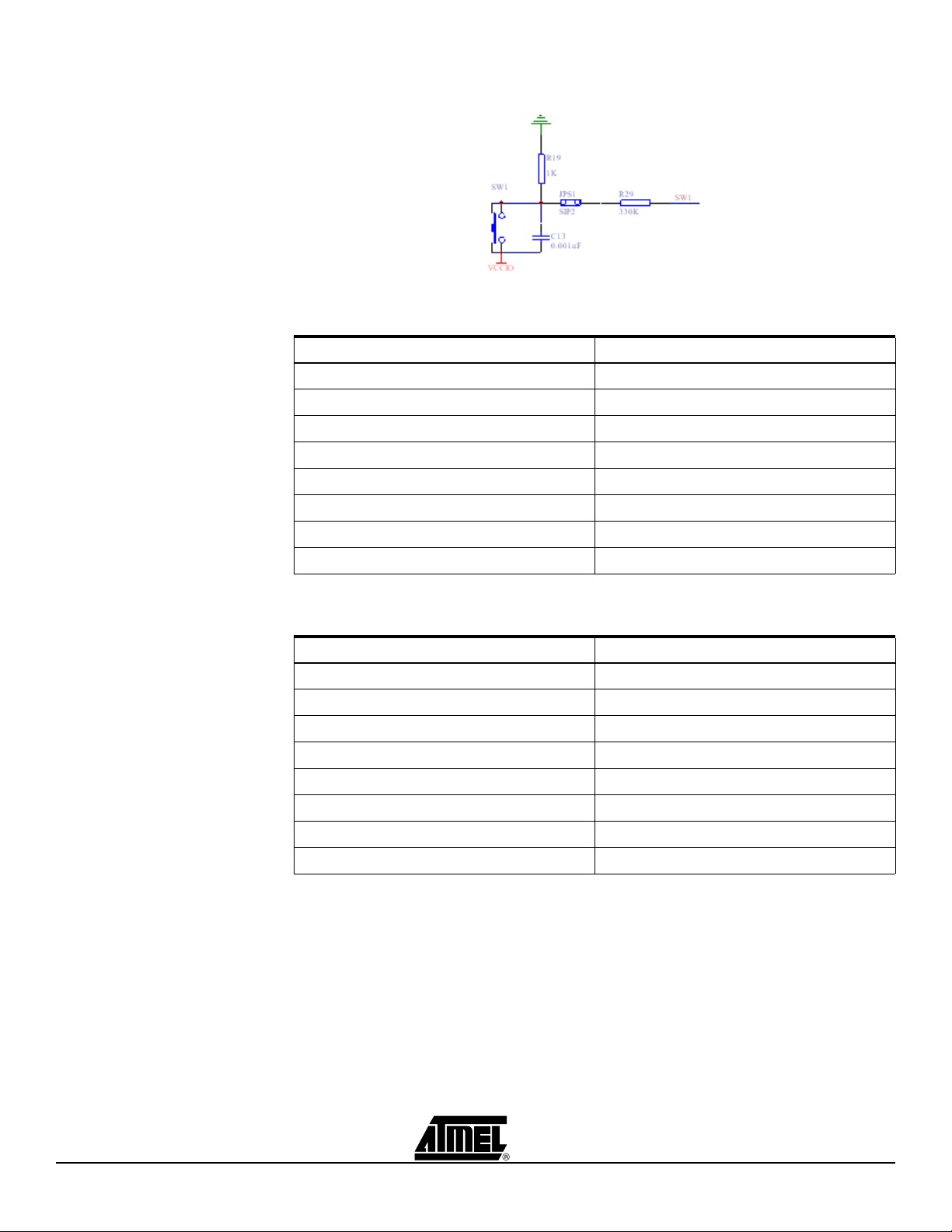
Atmel CPLD Development/Programmer Board contains eight push-button switches,
which are connected to the I/O pins of the CPLD. They allow designers to send input
logic signals to the user I/O pins of the ATF15xx CPLD. These eight switches are
labeled SW1 to SW8 on the Atmel CPLD Development/Programmer Board. One end of
each input push-button switch is connected to VCCIO while the other end of each pushbutton switch is connected to a pull-down resistor and then connected to the specific I/O
pin of the CPLD through the JPS1/JPS2/JPS3/JPS4/JPS5/JPS6/JPS7/JPS8 selectable
jumper.
If any one of these switches is pressed and the corresponding jumper is set, the specific
I/O pin of the device will be driven to a logic high state by the output of switch circuit.
Since each push-button switch is also connected to a pull-down resistor, the input will
have a logic low state if the switch is not pressed with the corresponding jumper set. If
the push-button jumper is not set, the corresponding pin will be treated as an unconnected pin. Figure 2-4 on page 2-7 is a circuit diagram of the push-button switch and
selectable jumper. Tables 2-9, 2-10, 2-11, and 2-12 show the connections of these eight
push-button switches to the CPLD I/O pins in the different package types.
2-6 ATF15xx-DK3 Development Kit User Guide
3605B–PLD–05/06
Page 14
Hardware Description
Figure 2-4. Circuit Diagram of the Push-button Switches and Jumpers for the I/O Pins
Table 2-9. Connections of ATF15xx 44-pin TQFP to the Switches for I/O Pins
Push Button # PLD Pin #
SW1 15
SW2 14
SW3 13
SW4 12
SW5 8
SW6 5
SW7 2
SW8 44
Table 2-10. Connections of ATF15xx 44-pin PLCC to the Switches for I/O Pins
Push Button # PLD Pin #
SW1 21
SW2 20
SW3 19
SW4 18
SW5 14
SW6 11
SW7 8
SW8 6
ATF15xx-DK3 Development Kit User Guide 2-7
3605B–PLD–05/06
Page 15

Hardware Description
Table 2-11. Connections of ATF15xx 84-pin PLCC to the Switches for I/O Pins
Push Button # PLD Pin #
SW1 54
SW2 51
SW3 49
SW4 44
SW5 9
SW6 6
SW7 4
SW8 80
Table 2-12. Connections of ATF15xx 100-pin TQFP to the Switches for I/O Pins
Push Button # PLD Pin #
SW1 48
SW2 36
SW3 44
2.1.4 Push-button
Switches with
Selectable Jumpers
for GCLR and OE1
Pins
SW4 37
SW5 96
SW6 98
SW7 84
SW8 99
Atmel CPLD Development/Programmer Board also contains two push-button switches
for the Global Clear (GCLR) and Output Enable (OE1) pins of the CPLD. They allow the
designers to control the logic states of the OE1 and GCLR inputs of the ATF15xx CPLD.
These two switches are labeled SW-GCLR and SW-GOE1 on the Atmel CPLD Development/Programmer Board. One end of the SW-GCLR input push-button switch is
connected to ground (GND). The other end of the push-button switch is connected to a
pull-up resistor to VCCIO, and then connected to the GCLR dedicated input pin of the
ATF15xx. It is intended to be used as an active-low reset signal to reset the registers in
the ATF15xx with the JPGCLR selectable jumper set. Similarly, one end of the SWGOE1 input push-button switch is connected to ground (GND). The other end of the
push-button switch is connected to a pull-up resistor to VCCIO, and then connected to
the OE1 dedicated input pin of the ATF15xx. It is intended to be used as an active-low
output enable signal to control the enabling/disabling of the tri-state output buffers in the
ATF15xx with the JPGOE selectable jumper set. Figure 2-5 on page 2-9 is the circuit
diagram of these two push-button switches and the jumpers for the GCLR and OE1
pins.
If any of these push-button switches is pressed and the corresponding jumper is set,
then the specific I/O of the CPLD will be driven to a logic low state. Since each pushbutton is also connected to a pull-up resistor, the corresponding CPLD input will have a
logic high state if the push-button switch is not pressed with the corresponding selectable jumper set. If the selectable jumper is not set, the corresponding dedicated input
pin of the CPLD can be considered a “no connect” (NC) pin. Table 2-13 on page 2-9
2-8 ATF15xx-DK3 Development Kit User Guide
3605B–PLD–05/06
Page 16

Hardware Description
shows the pin numbers of the GCLR and OE1 dedicated input pins of the ATF15xx in all
the different available package types.
Figure 2-5. Circuit Diagram of Push-button Switches and Selectable Jumpers for
GCLR and OE1
Table 2-13. Pin Numbers of GCLR and OE1
2.1.5 2 MHz Oscillator and
Clock Selection
Jumper
44-pin
TQFP
GCLR 39 1 1 89
OE1 38 44 84 88
44-pin
PLCC
84-pin
PLCC
100-pin
TQFP
The Clock Selection Jumper, labeled JP-GCLK, on the CPLD Development/Programmer Board is a two-position jumper that allows the users to select which GCLK
dedicated input pin (either GCLK1 or GCLK2) of the ATF15xx should be connected to
the output of the 2 MHz oscillator. In addition, the jumper can be removed to allow an
external clock source to be connected to GCLK1 and/or GCLK2 of the ATF15xx. Figure
2-6 is the circuit diagram of the oscillator and selection jumper. Table 2-14 on page 2-10
shows the pin numbers for the GCLK1 and GCLK2 dedicated input pins of the ATF15xx
in all the different available package types.
Note: If GCLK1 jumper is set, the jumper will be located toward the side of the board.
On the other hand, if GCLK2 jumper is set, the jumper will be located toward the
middle of the board.
Figure 2-6. Circuit Diagram of Oscillator and Clock Selection Jumper
ATF15xx-DK3 Development Kit User Guide 2-9
3605B–PLD–05/06
Page 17

Hardware Description
Table 2-14. Pin Numbers of GCLK1 and GCLK2
2.1.6 VCCIO and VCCINT
Voltage Selection
Jumpers and LEDs
44-pin
TQFP
GCLK1374383 87
GCLK2 40 2 2 90
44-pin
PLCC
84-pin
PLCC
100-pin
TQFP
The VCCIO and VCCINT Voltage Selection Jumpers, labeled VCCIO Selector and
VCCINT Selector respectively on ATF15xx-DK3 Development/Programming Board,
allow the designers to select I/O supply voltage level (VCCIO) and core supply voltage
level (VCCINT) that are used for the target CPLD on the board. Once these jumpers are
set correctly, the LEDs (labeled VCCINT LED and VCCIO LED) will be turn on as
expected. However, at lower supply voltage levels (i.e. 2.5V or lower), the LEDs might
be very dim.
For ATF15xxAS/ASL (5.0V) CPLDs, both the VCCIO Selector and VCCINT Selector
jumpers MUST BE set to 5.0V. For ATF15xxASV/ASVL (3.3V) CPLDs, both the VCCIO
Selector and VCCINT Selector Jumpers MUST BE set to 3.3V only. For the ATF15xxBE
(1.8V) CPLDs, designers MUST SET VCCINT Selector jumper to 1.8V for its core voltage supply. However, designers can set the VCCIO Selector jumper to 3.3V, 2.5V, or
1.8V (but not 5.0V) in order for the I/Os of the ATF15xxBE CPLD to interface with different voltage levels devices.
Note: The power of the CPLD Development/Programmer Board MUST BE turned
OFF when changing the position of the VCCIO or VCCINT voltage selection
jumper (VCCIO Selector or VCCINT Selector).
2.1.7 ICCIO and ICCINT
Jumpers
The IccIO and IccINT jumpers can be removed and used as Icc measurement points.
When the jumpers are removed, current meters can be connected to the posts to measure the current consumption of the target CPLD. When users are not using these
jumpers to measure the current, these jumpers must be set in order for the board and
CPLD to operate.
2.1.8 Voltage Regulators Two voltage regulators, labeled VR1 and VR2, are used to independently generate and
regulate the VCCINT and VCCIO voltages from the 9V DC power supply. For details,
please review the schematic of the ATF15xx-DK3 board.
2.1.9 Power Supply
Switch and Power
LED
The Power Supply Switch, labeled POWER SWITCH, can be switched to the ON or
OFF position, which is used to turn on or off the power of the ATF15xx-DK3 board
respectively. It allows the 9V DC voltage at the Power Supply Jack to pass to the voltage regulators when it is in the ON position. When the Power Supply Switch is turned
ON, the Power LED (labeled POWER LED) will light up to indicate that the ATF15xxDK3 board is supplied with power.
2.1.10 Power Supply Jack
and Power Supply
Header
The Atmel ATF15xx-DK3 Development/Programmer Board contains two different types
of power supply connectors labeled JPower and JP Power. Either one of these power
supply connectors can be used to connect a 9V DC power source to the board. The first
power connector, labeled JPower, is a barrel power jack with a 2.1mm diameter post
and it mates to a 2.1mm (inner diameter) x 5.5mm (outer diameter) female plug. The
second is the power supply header, labeled JP Power, is a 4-pin male 0.1" header with
0.025" square posts. The availability of these two types of power connectors allows the
users to choose the type of power supply equipment to use for ATF15xx-DK3 Development/Programmer Board. However, please note that only one of these two power
supply connectors should be powered with a 9V DC source but not both at the same
time.
2-10 ATF15xx-DK3 Development Kit User Guide
3605B–PLD–05/06
Page 18

Hardware Description
2.1.11 JTAG ISP Connector
and TDO Selection
Jumper
The JTAG ISP Connector, labeled JTAG-IN, is used to connect the ATF15xx’s JTAG
port pins (TCK, TDI, TMS and TDO) through the ISP download cable to the parallel
printer (LPT) port of a PC for JTAG ISP programming of the ATF15xx. Polarized connectors are used on the ATF15xx-DK3 and ISP Download Cable (ATDH1150VPC) Rev
6.0 or later to minimize connection problems. The PIN1 label at the bottom of the JTAG
ISP connector indicates the pin 1 position of the 10-pin header and further reduces the
chance of connecting the ISP Download Cable incorrectly.
To the left of the JTAG-IN connector, there are two columns of vias and they are labeled
JTAG-OUT. They are intended to allow the users to create a JTAG daisy chain to perform JTAG operations to multiple devices. Users will need to solder the same type of
connector as the one used for JTAG-IN into the JTAG-OUT position in order to utilize
this available feature.
To create a JTAG daisy chain using multiple ATF15xx-DK3 boards, the TDO Selection
Jumper, labeled JP-TDO, must be set to the appropriate position. For all the devices in
the daisy chain except the last device, this jumper must be set to the “TO NEXT
DEVICE” position. For the last device in the chain, this jumper must be set to the “TO
ISP CABLE” position. When this jumper is in the “TO NEXT DEVICE” position, the TDO
of that particular JTAG device will be connected to the TDI of the next JTAG device in
the chain. When this jumper is in the “TO ISP CABLE” position, the TDO of that device
will be connected to the TDO of the JTAG 10-pin connector, which will allow the TDO
signal of the that device in the chain to be transmitted back to the host PC with the ISP
software. Figure 2-7 below is a circuit diagram of the JTAG connectors and the JP-TDO
jumper. Table 2-15 on page 2-12 lists the pin numbers of the four JTAG pins for the
ATF15xx in all the available packages.
For a single device setup, the position of the JP-TDO jumper must be set to “TO ISP
CABLE”.
Figure 2-7. Circuit Diagram of the JTAG ISP Connectors and TDO Jumper
ATF15xx-DK3 Development Kit User Guide 2-11
3605B–PLD–05/06
Page 19

Hardware Description
Table 2-15. Pin Numbers of JTAG Port Signals
44-pin
TQFP
44-pin
PLCC
84-pin
PLCC
100-pin
TQFP
TDI 1 7 14 4
TDO323871 73
TMS 7 13 23 15
TCK263262 62
The ISP algorithm is controlled by the ATMISP software, which is running on the PC.
The four JTAG signals are generated by the LPT port and they are buffered by the ISP
download cable before going into the ATF15xx on the CPLD Development/Programmer
Board. The pinout for the 10-pin JTAG Port Header on the CPLD Development/Programmer Board is shown in Figure 2-8 and the dimensions of this 10-pin male JTAG
header are shown in Figure 2-9.
Figure 2-8. Pinout Diagram of 10-pin JTAG Port Header (Top-view)
GND
NC
NC
GND
10
8
6
4
2
TDI
9
7
NC
5
TMS
3
TDOVCC
1
TCK
2.2 Socket Adapter
Board
Figure 2-9. 10-pin Male Header Dimensions
Top View
0.100
0.100
Side View
0.025 Sq.
0.235
All dimensions are in inches
The pinout of this 10-pin JTAG Port Header is compatible with the Altera
®
ByteBlaster,
ByteBlasterMV, and ByteBlaster II cables. In addition, the ATMISP software allows
users to choose either the Atmel CPLD ISP Cable or the ByteBlaster/ByteBlasterMV/ByteBlaster II cable to implement ISP.
Atmel ATF15xx-DK3 CPLD Development/Programmer Socket Adapter Boards
(ATF15xx-DK3-XXXXX) are circuit boards that interface with the Atmel ATF15xx-DK3
CPLD Development/Programmer Board. They are used in conjunction with the
ATF15xx-DK3 CPLD Development/Programmer Board to evaluate/program Atmel
ATF15xx ISP CPLDs with different package types. At press time, there are four Socket
Adapter Boards available for the ATF15xx-DK3 covering the 44-TQFP, 44-PLCC, 84-
2-12 ATF15xx-DK3 Development Kit User Guide
3605B–PLD–05/06
Page 20

Hardware Description
PLCC, and 100-TQFP package types in the ATF15xx family of CPLDs. Socket Adapter
boards for other packages will become available in the near future.
Each socket adapter board contains a socket for the Atmel ATF15xx device and with
male headers on the bottom side, labeled JP1 and JP2. The headers on the bottom side
mate with the female headers on the ATF15xx-DK3 board, labeled JP4 and JP3. The
four 7-segment displays, push-button switches, JTAG port signals, oscillator, VCCINT,
VCCIO, and GND on the CPLD Development/Programmer Board are connected to the
ATF15xx device on the Socket Adapter Board through these two sets of connectors.
On the top of the 44-TQFP socket adapter, there are four 10-pin connectors with the
same dimensions as the JTAG ISP connector. The pins of these four connectors are
connected to the input and I/O pins (except the four JTAG pins) of the target CPLD
device. They can be used to connect to an oscilloscope or logic analyzer to capture the
activities of the input and I/O pins of the CPLD. They also can be used to connect the
input and I/O pins of the CPLD to other external boards or devices for system level evaluation or testing.
2.3 Atmel CPLD ISP
Download Cable
The Atmel CPLD ISP Download Cable (P/N: ATDH1150VPC) connects the parallel
printer (LPT) port of your PC to the 10-pin JTAG header on the Atmel CPLD Development/Programmer Board or a custom circuit board. This is shown in Figure 2-10 on
page 2-14. This ISP cable acts as a buffer to buffer the JTAG signals between the PC’s
LPT port and the ATF15xx on the circuit board. The Power-On LED on the back of the
25-pin male connector housing indicates that the cable is connected properly. Make
sure this LED is turned on before using the Atmel CPLD ISP Software (ATMISP).
This ISP cable consists of a 25-pin (DB25) male connector, which is connected to the
LPT port of a PC. The 10-pin female plug connects to the 10-pin male JTAG header on
the ISP circuit board. The red color stripe on the ribbon cable indicates the orientation of
Pin 1 of the female plug. The 10-pin male JTAG header on the CPLD Development/Programmer Board is polarized to prevent users from inserting the female plug in the wrong
orientation.
The Atmel CPLD Development/Programmer kits includes an Atmel ISP cable; however,
other supported ISP cables can also be used. The use of the ISP cable on Atmel development kit is depending on the device that is selected.
The following shows the appropriate ISP cable that can be used for the different voltage
families of Atmel CPLDs.
1. Atmel-ISP Cable (Rev 4.0 or earlier) can be used for ATF15xxAS/ASL (5.0V)
device only.
2. Atmel-ISP Cable (Rev 5.0) can be used for ATF15xxAS/ASL (5.0V) or
ATF15xxASV/ASVL (3.3V) device only.
3. Atmel-ISP Cable (Rev 6.0), also known as the “Atmel CPLD-ISP MV Cable”,
can be used for ATF15xxAS/ASL (5.0V) or ATF15xxASV/ASVL (3.3V) or
ATF15xxBE (1.8V core) device.
4. ByteBlaster ISP Cable can be used for ATF15xxAS/ASL (5.0V) device only.
5. ByteBlasterMV ISP Cable can be used for ATF15xxAS/ASL (5.0V) or
ATF15xxASV/ASVL (3.3V) device only.
6. ByteBlaster II ISP Cable can be used for ATF15xxAS/ASL (5.0V) or
ATF15xxASV/ASVL (3.3V) or ATF15xxBE (1.8V core) device.
ATF15xx-DK3 Development Kit User Guide 2-13
3605B–PLD–05/06
Page 21

Hardware Description
Figure 2-10. Atmel ISP Cable Connection to ISP Hardware Board/Circuit Board
ISP
CABLE
DOWNLOAD
Color
Stripe
LED
Pin 1
Figure 2-11 shows the pinout for the 10-pin female header on the Atmel ISP cable. The
pinout on the 10-pin male header on the PC board (if used for ISP) must match this
pinout.
Figure 2-11. Atmel ISP Download Cable 10-pin Female Header Pinout
Color Stripe
1 3 579
1 3 579
246 8 10
246 8 10
Note: Your circuit board must supply Vcc and GND to the Atmel CPLD ISP Cable
through the 10-pin male header. When programming ATF15xxBE device,
VCCIO must be used for the ISP Cable.
2-14 ATF15xx-DK3 Development Kit User Guide
3605B–PLD–05/06
Page 22

Section 3
CPLD Design Flow Tutorial
This tutorial will guide you through a complete VHDL design cycle for the Atmel
ATF15xx CPLD. It provides step-by-step procedure to go through each phase of the
design cycle from design entry, logic synthesis, device fitting, in-system programming,
and finally verifying the design on the Atmel ATF15xx-DK3 CPLD Development/Programming Board.
Note: To complete this tutorial, ProChip Designer V4.0 with Level 2 Update and
Atmel-ISP Software (ATMISP) V6.1 are required.
3.1 Create a Project
using the “New
Project Wizard”
Before starting the design process, a Project File must be created within ProChip
Designer. ProChip Designer’s New Project Wizard provides a very easy way to create a
new project file.
ATF15xx-DK3 Development Kit User Guide 3-1
3605B–PLD–05/06
Page 23

CPLD Design Flow Tutorial
1. Click on the Start > Programs > ProChip icon to launch ProChip Designer. Or
double-click on the ProChip icon on the desktop.
(1) Click to
launch
ProChip
Designer
2. Click on Project > New or double-click on the New Project shortcut button to
launch the New Project Wizard.
(2) Click to
create ne
project
w
3. Click on the Next button to start the project file creation process.
(3) Click Next
to start
4. Click on the Browse button to open the browser window.
3-2 ATF15xx-DK3 Development Kit User Guide
3605B–PLD–05/06
Page 24

CPLD Design Flow Tutorial
5. Use C:\PROCHIP\DESIGNS\VHDL as the directory of the project.
6. Enter DEV_KIT.APJ as the project filename. The extension of a project file must
be .APJ.
Note: The name and directory of the design project is specified in this window. All
design, simulation, and other project files must be placed in this project directory.
(4) Click to
Browse
(5) Select the
project directory
(6) Enter the project
filename
7. Choose ATF1502BE-7AU44 as the target device type for the project. Also review
the filters that allow for selection of a specific speed grade or package type.
(7) Select the
device type
ATF15xx-DK3 Development Kit User Guide 3-3
3605B–PLD–05/06
Page 25

CPLD Design Flow Tutorial
8. Select VHDL - Mentor Graphics as the software tool for this design flow.
(8) Select the
design flow
ProChip Designer V4.0 with software patch level 1 and later version supports the following design flows:
Design Flow Design Flow Type
CUPL – Altium CUPL design compiled through Altium Protel 99SE
Verilog – Mentor Graphics Verilog design synthesized through Mentor Graphics Precision
VHDL – Altium VHDL design synthesized through the Altium PeakFPGA
VHDL – Mentor Graphics VHDL design synthesized through Mentor Graphics Precision
Schematic – Altium Schematic design compiled through Altium Protel 99SE
9. Select Done with parts so that there will be only one device in this project.
3-4 ATF15xx-DK3 Development Kit User Guide
3605B–PLD–05/06
Page 26

CPLD Design Flow Tutorial
On the other hand, users can select Add more parts to include more parts to the current project directory.
(9) Select Done
with parts
10. Click the Finish button to finish the New Project Wizard and the project creation
process.
This closes the New Project Wizard and opens the ProChip Designer window. The
sources in the project are shown in the left window.
(10) Select Finish
to end the New
Project Wizard
ATF15xx-DK3 Development Kit User Guide 3-5
3605B–PLD–05/06
Page 27

CPLD Design Flow Tutorial
11. Click on the ATF1502BE-7AU44 device icon to view the Design Flow window.
Project Sources window Information dialog box
(11) Click on the device iconMessage window
Project File window Design Flow window
3-6 ATF15xx-DK3 Development Kit User Guide
3605B–PLD–05/06
Page 28

CPLD Design Flow Tutorial
3.2 Add a Design
File
Once the project file is created, the next step is to add the design source file(s) into your
project. For this tutorial, a single VHDL design file will be added into the project.
1. Click on the Add/Edit button from Source Manager to open the Source Manager
window. You can view the Source Manager help file by clicking on the Help button within the Source Manager window to view the description for the different
processes.
2. In the Source Manager window, click on the Add button to add a VHDL design
file to the project.
3. In the File Manager window, select .VHD from the C:\PROCHIP\DESIGNS\VHDL directory as the source design file for this project.
(1) Click Add/Edit
to open Source
Manager window
(2) Select VHDL
source file
3.3 Synthesize the
VHDL Design
(3) Click Add to
add design file
This VHDL design is available at the end of this document.
The F02_44TQFP.VHD file is a VHDL design that uses two 7-segment displays and the
built-in oscillator on the Atmel ATF15xx-DK3 CPLD Development/Programmer Board to
generate two scrolling “0” characters. This design will also pass the states of the I/O
push-button switches (SW1-SW4) to the LEDs at LED1-LED4 on the ATF15xx-DK3
CPLD Development/Programmer Board. For details, please review the VHDL code.
In this part of the tutorial, the VHDL design code will be synthesized through the Mentor
Graphics Precision Synthesis process into an EDIF netlist (*.EDF), which contains a set
of optimized/minimized logic equations for the specified CPLD.
ATF15xx-DK3 Development Kit User Guide 3-7
3605B–PLD–05/06
Page 29

CPLD Design Flow Tutorial
1. Click on the VHDL - Precision button in the Design Flow window to open the
Logic Synthesis window.
(1) Open the Logic
Synthesis window
2. In the Logic Synthesis window, check both options to Update Pin Assignments
after each Compilation and also Run Precision in shell mode:
3.4 Fit the
Synthesized
Design File
(2) Check
both options
here
3. Click on the Compile button to start the compile process. Close the log file when
the synthesis is done successfully.
Note: If you have encountered any syntax error during synthesis, the report file will
pop up to indicate which line of the code contains problem. In such case, you
must correct the syntax problem and save the file before synthesize the code
again before proceeding to the next step.
In Section 3.3, the logic synthesis portion of the CPLD design flow was completed. On
successful compilation, the Precision tool will produce an EDIF output file (with .EDF
extension). An EDIF file contains the netlist of the optimized and minimized logic equations. We now need to map this netlist into a specific Atmel CPLD architecture using the
Atmel Fitter.
3-8 ATF15xx-DK3 Development Kit User Guide
3605B–PLD–05/06
Page 30

CPLD Design Flow Tutorial
1. You can now proceed to the device fitter portion of the design flow by clicking on
the Atmel Fitter button.
(1) Open the Atmel
Fitter window
You can either use the default options or specify fitter properties. ProChip Designer will
automatically select the EDIF file (*.EDF) associated to the current design project and
the tool type. In this example, since our target device is an ATF1502BE, we will select
the FIT1502.EXE device fitter.
The fitter creates the important JEDEC and Fit Report output files. They contain the data
for programming the device (using in-system programming or on a third-party device
programmer) and the pin assignments required for board layout respectively.
Please review the Global Device Parameters and Pin/Node Options as well. The help
files also show the Device Pin_Node lists for each of the Atmel CPLDs.
2. Make sure the JTAG box is checked. This enables the JTAG port for ISP
programming.
3. Make sure the Pin Fit Control setting is set to Keep. This will ensure that the pin
assignments in the PLD file will be kept during the place-and-route process.
4. Make sure the Logic Double setting is set to if necessary.
5. When all the fitter options are set, click on the Run Fitter button to fit the design.
(2) Check the
JTAG box
(3) Set the Pin
Fit Control
setting to
Keep
(5) Start the fitting
process
(4) Set Logic Double
to if necessary
ATF15xx-DK3 Development Kit User Guide 3-9
3605B–PLD–05/06
Page 31

CPLD Design Flow Tutorial
The above message will be displayed after the design is successfully fit the selected
device.
If there are any error messages, you can review the exported *.FIT file or you can copy
your *.EDF file to the C:\PROCHIP\PLDFIT\ directory, open the DOS command prompt,
and then type the fit command that is starting from the second line of the *.FIT file to see
more details about the fitter errors.
Parts of the fitter report (.FIT) file generated for this design is shown below.
Total dedicated input used: 3/4 (75%)
Total I/O pins used 24/32 (75%)
Total Macro cells used 35/32 (109%)
Total Flip-Flop used 28/32 (87%)
Total Foldback logic used 15/32 (46%)
Total Nodes+FB/MCells 50/32 (156%)
Total cascade used 0
Total input pins 10
Total output pins 17
Total Pts 93
Creating pla file c:\Prochip\designs\vhdl\f02_44TQFP.tt3 with 0 inputs 0
outputs, 0 pins 0 nodes and 0 pterms...
3.5 Program and
Verify Design
---------------- End fitter, Design FITS
$Device TQFP44 fits
FIT1502 completed in 0.00 seconds
In this step of the tutorial, you will program an ATF1502BE 44-pin TQFP device on the
Atmel ATF15xx-DK3 CPLD Development/Programmer Board through ISP. Then you will
be able to verify the design by observing the four 7-segment displays and four LEDs on
the CPLD Development/Programmer Board.
You will need to follow the steps below to setup the ATMISP software (V6.0 or latest
version) in order to program the ATF1502BE 44-pin TQFP on the ATF15xx-DK3 CPLD
Development/Programmer Board.
3-10 ATF15xx-DK3 Development Kit User Guide
3605B–PLD–05/06
Page 32

CPLD Design Flow Tutorial
1. To create a new chain file, the ATMISP Software first needs to be launched either
through the Program Chip button in the ProChip Designer window, the ATM ISP
desktop icon or the Start > Programs > Atmel-ISP menu.
(1) Launch
ATMISP
Note: If ATMISP is launched through ProChip Designer, then the appropriate chain
(.CHN) file will be automatically created by ProChip Designer. Therefore, steps
2 through 6 can be skipped.
2. To create a new chain file, select the New command under the File menu or click
on the New shortcut button.
(2) Create new
chain file
3. The first piece of information that the software asks for when creating a new
chain is the number of devices in the JTAG chain. Therefore, enter “1” and then
click OK since you will be programming a single-device JTAG chain.
(3) Enter the
number of
devices
4. Next you will need to specify the properties of each JTAG device in the Device
Properties window. First, you will need to select the target device type of the first
device in the JTAG chain. For this tutorial, please select ATF1502BE as the target device type.
5. In the JTAG Instruction field, you can specify which JTAG instruction to be executed on this device in the chain. Please select Program/Verify to program and
verify the ATF1502BE.
6. The next step is to specify the JEDEC file to be programmed into the target
device in the JEDEC File field. Click on the Browse button, change the directory
to ..\PROCHIP\DESIGNS\VHDL and then select F02_44TQFP.JED as the
ATF15xx-DK3 Development Kit User Guide 3-11
3605B–PLD–05/06
Page 33

CPLD Design Flow Tutorial
JEDEC file. Click OK to close the JTAG Device Properties window when all properties are specified.
(4) Specify target
device type
(5) Specify JTAG
instruction
(6) Select JEDEC
file
The next step requires you to setup the Atmel ATF15xx-DK3 CPLD Development/Programmer Board to program the ATF1502BE-7AU44 through the CPLD ISP cable.
7. Connect the DB25 side of the Atmel CPLD ISP MV cable (Revision 6) to the PC’s
parallel port and the 10-pin header side of the cable to the Atmel ATF15xx-DK3
CPLD Development Board as shown Figure 2-10 on page 2-14.
8. Connect a 9V AC/DC power supply to the power connector (JPower) of the Atmel
ATF15xx-DK3 CPLD Development/Programmer Board.
9. Set the VCCIO Selector jumper to the 1.8V(BE) position for supplying the core
voltage of the ATF1502BE device at 1.8V, then set the VCCINT Selector jumper
to the 1.8V(BE) position for supplying the I/O pad voltage of the ATF1502BE
device at 1.8V.
Note: Make sure the ICCINT and ICCIO jumpers are in their default positions. These
two jumpers are only removed when you are connecting them from two poles of
the digital multimeter to perform current measurement.
10. Set the JPCLK jumper to GCLK1 so that the output of the crystal oscillator will go
to pin 37 (GCLK1) of the ATF1502BE. For this design, you can also set the
JPCLK jumper to GCLK2 so that the output of the crystal oscillator will go to pin
40 (GCLK2) of the ATF1502BE for selecting another global clock source.
11. Set the JPJTAG Jumper ISP Cable position, which is toward the middle of the
board.
12. Connect the 44-pin TQFP Socket Adapter Board onto the main development/programmer board.
Note: If a device in a different package type is to be programmed, then the appropri-
ate Socket Adapter Board must be used.
13. Select which LPT port is being used for Atmel CPLD ISP cable in the Port Setting
field. LPT1 is the default port and it represents address 0x378.
14. Select the ISP download cable type in the Cable Type field. The default cable
type is the “Atmel CPLD-ISP MV”, which represents the Atmel CPLD ISP Cable
Rev 6.0, but it can be changed to other cables that can be used for other devices.
Note: The “Atmel CPLD-ISP” cable type represents the Atmel CPLD ISP Cable Rev
5.0 or older.
15. Switch the power switch to the ON position.
3-12 ATF15xx-DK3 Development Kit User Guide
3605B–PLD–05/06
Page 34

CPLD Design Flow Tutorial
Now both your software and hardware are setup for ISP programming and you can execute the Program/Verify instruction to program the ATF1502BE on the Atmel ATF15xxDK3 CPLD Development/Programmer Board.
16. Click on the Run button in the ATMISP main window to execute the JTAG
instruction to program the ATF1502BE on ATF15xx-DK3 CPLD Development/Programmer Board.
(13) Select the
LPT port
number
(14) Select the
cable type
(16) Click on the
Run button
If you do not see above message after programming of the device, please review the
troubleshooting guide and FAQs from the Atmel-ISP software to debug the problem.
After successfully programming the ATF1502BE with the F02_144TQFP.JED file, the
first and fourth 7-segment LED displays should show two rotating “0” characters. In
addition, with the setting of the LED jumpers (JPL1, JPL2, JPL3, and JPL4) and pushbutton jumpers (JPS8, JPS7, JPS6, and JPS5), you can press SW8, SW7, SW6, or
SW5 to light up LEDs 1-4.
If the result is displayed correctly on the ATF15xx-DK3 CPLD Development/Programmer Board, then you have successfully completed this tutorial.
ATF15xx-DK3 Development Kit User Guide 3-13
3605B–PLD–05/06
Page 35

Section 4
Schematic Diagrams and VHDL File
ATF15xx-DK3 Development Kit User Guide 4-1
3605B–PLD–05/06
Page 36

Schematic Diagrams and VHDL File
Figure 4-1. ATF15xx-D3 Development/Programmer Board Schematic Diagram
SW4
R35
4.7K
JPS4
SIP 2
C19
R25
0.001uF
1K
SW8
R36
4.7K
JPS8
SIP 2
C20
R26
0.001uF
1K
VccIOVccI O
R14
10K
R13
4.7K
R12
4.7K
R11
4.7K
TMS
TCK
TDO
TDI
123
JPJTAG
VCCIO
SW4
SW3
R33
LED8
GREEN
JPL8
RL8
220
RL7
220
RL6
220
RL5
220
RL4
220
RL3
220
RL2
220
RL1
220
SIP 2
LED8
LED7
GREEN
JPL7
SIP 2
LED7
LED6
GREEN
JPL6
SIP 2
LED6
LED5
GREEN
JPL5
SIP 2
LED5
LED4
GREEN
JPL4
SIP 2
LED4
LED3
GREEN
JPL3
SIP 2
LED3
LED2
GREEN
JPL2
SIP 2
LED2
LED1
GREEN
JPL1
SIP 2
LED1
4.7K
JPS3
SIP 2
C17
R23
R21
R19
0.001uF
1K
SW3
SW2
R31
4.7K
JPS2
SIP 2
1K
SW2
SW1
R29
4.7K
JPS1
SIP 2
1K
SW1
R24
VCCIO
C15
0.001uF
R22
VCCIO
C13
0.001uF
R20
VCCIO
VCCIO
SW8
SW7
R34
4.7K
JPS7
SIP 2
C18
0.001uF
1K
VCCIO
SW7
SW6
R32
4.7K
JP2
JPS6
SIP 2
C16
0.001uF
1K
VCCIO
SW6
SW5
R30
4.7K
JPS5
SIP 2
C14
0.001uF
1K
SW5
VCCIO
IccINT
C6
C5
0.1uF
R7
500
2
+Vout
ADJ
1
Vin
LM317 Vcc I NT
VR2
3
VCCIN
R27
1K
D3
10uF
R8
220
12
34
56
78
910
JTAGIN
3
2
1
JPGCLK
R9
600
R10
680
JPINT33
3.3V(ASV)
JPINT18
1.8V(BE)
12
34
56
78
910
JTAGOUT
R18
1K
R39
100
R17
1K
GCLK2 GCLK1
14
23
OSC
2MHZ
C21
0.1uF
VccIO
JPINT50
5.0(AS)
DOT4
DOT3
DOT2
DOT1
GNDGND
12
34
JP3
VCCINT GND
RDOT2 RDOT3 RDOT4
RDOT1
DOT1
LED1
LED2
LED3
56
78
910
11 12
D1A
D1B
D1C
D1F
DOT
Vc2
DSP4
JPDSP4
JPLED4
Vc1
DOT
Vc2
DSP3
JPDSP3
JPLED3
Vc1
DOT
Vc2
DSP2
JPDSP2
JPLED2
Vc1
DOT
Vc2
DSP1
JPDSP1
JPLED1
Vc1
VccIO
SW1
SW2
SW3
SW4
DOT2
LED4
TDO
13 14
15 16
17 18
19 20
21 22
23 24
25 26
27 28
29 30
31 32
33 34
35 36
37 38
39 40
TCK
D1D
D1E
D1G
VCCIO GND
D2A
D2B
D2C
D2D
D2E
D2F
D2G
GND GND
g
f
c
b
e
d
g
d
a
c
e
f
b
a
g
f
c
b
e
d
g
d
a
c
e
f
b
a
g
f
c
b
e
d
g
d
a
c
e
f
b
a
g
f
c
b
e
d
g
d
a
c
e
f
b
a
D4D
D4E
D4F
D4G
TDI
VCCIN TGND
12
34
56
78
910
11 12
JP4
SW8
GCLK1
GND GND
GCLK2
GCLR
GOE
RDSP47
RDSP45
RDSP43
RDSP41
RDSP37
RDSP35
RDSP33
RDSP31
RDSP27
RDSP25
RDSP23
RDSP21
RDSP17
RDSP15
RDSP13
RDSP11
D4A
13 14
SW7
D4G
D4F
RDSP46
D4E
D4D
RDSP44
D4C
D4B
RDSP42
D4A
D3G
D3F
RDSP36
D3E
D3D
RDSP34
D3C
D3B
RDSP32
D3A
D2G
D2F
RDSP26
D2E
D2D
RDSP24
D2C
D2B
RDSP22
D2A
D1G
D1F
RDSP16
D1E
D1D
RDSP14
D1C
D1B
RDSP12
D1A
D4B
D4C
D3A
D3B
D3C
D3D
D3E
D3F
D3G
TMS
15 16
17 18
19 20
SW5
SW6
DOT4
VCCIOGND
21 22
23 24
25 26
27 28
29 30
31 32
33 34
35 36
37 38
39 40
DOT3
LED5
LED6
LED7
LED8
GND GND
JP1
IccIO
C4
10uF
C3
0.1uF
R2
500
2
+Vout
ADJ
1
Vin
LM317 VccI O
VR1
3
VccIN
4
3
2
1
JP
JP Power
R1
1K
D2
R3
220
R4
280
R5
320
R6
680
JPIO33
3.3V(ASV/BE)
JPIO25
JPIO18
1.8V(BE)
R28
1K
D4
C2
0.1uF
C1
100uF
POWER SWITCH
D1
1N4001
9VDC
500mA
JPower
9V DC Center Positive
2.5V(BE)
GOE
R38
R16
1K
R15
1K
VccI O
JPGCLR JPGOE
R37
GCLR
BIGATMEL
MARK
ATMEL
JPIO50
5V(AS)
C11
0.1uF
C12
0.1uF
VccI NT
C10
0.1uF
C9
0.1uF
VccI O
2.2K
C8
0.001uF
SW-GOE
SW-GOE
SW-GCL R
SW-GCL R
C7
0.001uF
2.2K
4-2 ATF15xx-DK3 Development Kit User Guide
3605B–PLD–05/06
Page 37

Figure 4-2. 44-pin TQFP Socket Adapter Board Schematic Diagram
PIN12
PIN13
PIN14
PIN25PIN27
PIN28PIN30
PIN31PIN33
PIN19PIN20
PIN22
PIN15
PIN25PIN27
PIN28PIN30
PIN31PIN33
Schematic Diagrams and VHDL File
GNDGND
DOT1
LED1
12
34
56
78
910
JP2
VCCINT GND
D1 B
D1 C
12
JT
TDO
LED2
LED3
LED4
11 12
13 14
15 16
17 18
19 20
D1 A
D1 D
D1 E
D1 F
D1 G
PIN23
PIN18
PIN21
34
56
78
910
PIN34 PIN35
PIN37 PIN38
PIN39 PIN40
PIN42 PIN43
PIN44
DOT2
SW1
SW2
SW3
SW4
12
34
56
78
910
JR
21 22
23 24
25 26
27 28
29 30
31 32
33 34
35 36
37 38
39 40
PIN23
GND GNDGND GND
TCK
D2 A
D2 B
D2 C
D2 F
VCCIO GND
D2 D
D2 E
D2 G
VCCI O
PIN3 4
PIN3 5
GND
PIN3 7
PIN3 8
PIN3 9
PIN4 0
VCCIN T
PIN4 2
PIN4 3
PIN4 4
TDO
PIN33
32
33
U1
I/O
TDO
I/O
34
GCLK3
35
GND
36
GCLK1
37
OE1
38
GCLR
39
I/OE2/GCLK2
40
VCC
41
I/O
42
I/O
43
I/O
44
TDI1I/O2I/O3GND4I/O5TMS7I/O8VCC9I/O10I/O
PIN31
31
TCK
GND
PIN23
PIN25
PIN27
PIN28
PIN30
23
24
25
26
28
29
I/O
I/O27I/O
I/O30I/O
TCK
VCC
ATMEL TQFP44
I/O
6
GND
GND
I/O
VCC
I/O
I/O
I/O
I/O
I/O
I/O
I/O
I/O
I/O
TQFP44
22
21
20
19
18
17
16
15
14
13
12
11
MARK
VCCINT
GND
BIGATMEL
ATMEL
PIN2 2
PIN2 1
PIN2 0
PIN1 9
PIN1 8
PIN1 5
PIN1 4
PIN1 3
PIN1 2
12
34
56
78
910
JB
PIN12 PIN13
PIN14 PIN15
PIN18 PIN19
PIN20 PIN21
PIN22
c4
0.1uF
VCCI N T
c3
0.1uF
c2
0.1uF
c1
0.1uF
VCCI O
PIN34
PIN35
D4 E
D4 G
VCCINTGND
12
34
56
78
910
JP1
GND GND
GCLR
GOE
PIN38
PIN39
PIN2
PIN3
PIN5
PIN6
PIN8
PIN10
TDI
PIN42
PIN43
TDI
TMS
D4 A
D4 B
D4 C
D4 D
D4 F
11 12
13 14
15 16
17 18
19 20
SW5
SW6
SW7
SW8
GCLK1
GCLK2
PI N2 PI N3
PI N5 PI N6
PI N8 PI N10
PIN44
PIN37
PIN40
D3 D
D3 E
D3 F
D3 G
21 22
23 24
25 26
27 28
29 30
LED6
LED7
LED8
DOT4
PIN11
VCCIOGND
D3 A
D3 B
D3 C
31 32
33 34
35 36
37 38
39 40
LED5
DOT3
GND
12
34
56
JL
PI N2 P IN3
PI N5 P IN6
PI N8 P IN10
PIN11
TMS
VCCI O
78
910
PIN11
ATF15xx-DK3 Development Kit User Guide 4-3
3605B–PLD–05/06
Page 38

Schematic Diagrams and VHDL File
Figure 4-3. 44-pin PLCC Socket Adapter Board Schematic Diagram
PIN18
PIN19
PIN20
PIN34PIN36
PIN37PIN39
GNDGND
DOT1
LED1
12
34
56
78
910
JP2
VCCINT GND
D1 B
D1 C
PIN31PIN33
PIN25PIN26
PIN28
TDO
LED3
LED4
LED2
11 12
13 14
15 16
D1 A
D1 D
D1 F
D1 G
PIN29
PIN27
12
34
JT
PIN40 PIN41
PIN43 PIN44
17 18
D1 E
PIN24
56
PIN1 PIN2
PIN21
SW1
DOT2
19 20
21 22
23 24
25 26
27 28
29 30
TCK
D2 A
D2 B
D2 C
78
910
PIN4 PIN5
PIN6
SW2
SW3
SW4
12
34
56
TDO
PIN39
38
39
U1
I/O
TDO
I/O
GCLK3
GND
GCLK1
OE1
GCLR
I/OE2 /GCLK2
VCC
I/O
I/O
I/O
I/O8I/O
TDI
7
JR
PIN37
37
9
I/O36I/O
GND
PIN29 PIN31
PIN33 PIN34
PIN36 PIN37
VCCIO
PIN34
PIN36
34
35
VCC
I/O
I/O
10
11
12
31 32
33 34
35 36
37 38
39 40
VCCIO GND
GND GNDGND GND
D2 D
D2 E
D2 F
D2 G
PIN4 0
40
PIN4 1
41
GND
42
PIN4 3
43
PIN4 4
44
PIN1
1
PIN2
2
VCCINT
3
PIN4
4
PIN5
5
PIN6
6
78
910
PIN39
GND
TCK
PIN29
PIN31
PIN33
29
30
31
32
I/O
I/O
I/O33I/O
TCK
GND
I/O
I/O
I/O
I/O
I/O
VCC
GND
I/O
I/O
ATMEL PLCC44
I/O
I/O
I/O
I/O16I/O
TMS
VCC
13
14
15
17
P LCC4 4
28
27
26
25
24
23
22
21
20
19
18
PIN2 8
PIN2 7
PIN2 6
PIN2 5
PIN2 4
VCCINT
GND
PIN2 1
PIN2 0
PIN1 9
PIN1 8
12
34
56
78
910
JB
PIN18 PIN19
PIN20 PIN21
PIN24 PIN25
PIN26 PIN27
PIN28
PIN8
PIN9
PIN11
PIN12
PIN14
PIN16
PIN17
TDI
GND
TMS
VCCIO
PIN40
PIN41
PIN4
PIN5
c4
0.1uF
D4 E
D4 F
D4 G
VCCINTGND
12
34
56
78
910
JP1
GCLK2
GCLR
GND GND
GOE
PIN44
PIN1
PIN2
TDI
TMS
D4 A
D4 B
D4 C
D4 D
11 12
13 14
15 16
SW7
SW8
GCLK1
PIN43
PI N8 PI N9
PIN6
D3 E
D3 F
D3 G
17 18
19 20
21 22
23 24
25 26
27 28
29 30
LED7
LED8
SW5
SW6
DOT4
PIN11 PIN12
PIN14 PIN16
PIN17
VCCIOGND
D3 A
D3 B
D3 C
D3 D
31 32
33 34
35 36
37 38
39 40
12
34
56
78
910
JL
LED5
LED6
DOT3
PIN8 PIN9
PIN11 PIN12
PIN14 PIN16
PIN17
VCCINTVCCIO
c3
0.1uF
c2
0.1uF
c1
0.1uF
4-4 ATF15xx-DK3 Development Kit User Guide
3605B–PLD–05/06
Page 39

Figure 4-4. 84-pin PLCC Socket Adapter Board Schematic Diagram
PIN39PIN40
PIN41PIN44
PIN45PIN46
PIN48PIN49
PIN50PIN51 PIN52
PIN56
PIN54
PIN51
PIN49
PIN69PIN70
PIN73PIN74
GNDGND
DOT1
LED1
12
34
56
78
910
JP2
D1B
D1C
VCCINT GND
PIN60PIN61
PIN64PIN65
PIN67PIN68
LED2
LED3
LED4
11 12
13 14
15 16
17 18
19 20
21 22
23 24
D1A
TCK
D1D
D1E
D1F
D1G
PIN58
PIN63
PIN44
DOT2
SW1
SW2
SW3
SW4
25 26
27 28
29 30
31 32
33 34
35 36
37 38
39 40
IDC40
GND GND
D2A
D2B
D2C
PIN57
PIN55
VCCIO GND
D2D
D2E
D2F
D2G
PIN48
PIN41
PIN50
PIN45
12
34
56
JP5
PIN69 PIN70
PIN73 PIN74
PIN56PIN57
78
910
11 12
13 14
PIN58 PIN60
PIN61 PIN63
PIN64 PIN65
PIN67 PIN68
PIN54PIN55
15 16
17 18
JPBOTTOM
Schematic Diagrams and VHDL File
C8
0.1uF
VCCIO
C7
0.1uF
C5
0.1uF
C3
0.1uF
C6
0.1uF
VCCI N T
C4
0.1uF
PIN2PIN4
PIN5PIN6
PIN8PIN9
PIN10PIN11
12
34
56
78
JP3
VCCINTGND
910
11 12
PIN1 PIN84
PIN75
D4G
PIN37
VCCIO
TDO
GND
PIN68
PIN69
PIN70
PIN73
PIN74
70
71
72
SMALLATMEL
MARK 1
PIN75
PIN76
PIN77
PIN76PIN77
PIN79PIN80
PIN81
13 14
15 16
17 18
PIN83
PIN75
PIN79
PIN77
PIN5
PIN76
TDI
D4A
D4D
D4E
D4F
VCCIO
PIN79
PIN80
PIN81
GND
PIN83
PIN84
PIN1
PIN2
JPTOP
VCCINT
PIN4
PIN5
PIN6
GND
PIN8
PIN9
PIN10
PIN11
PIN10
PIN12
PIN16
PIN21
PIN17
PIN25
PIN22
TMS
D4B
D4C
D3A
D3B
D3C
D3D
D3E
D3F
D3G
74
U1
I/O73I/O
I/O
75
I/O
76
I/O
77
VCC_I O
78
I/O
79
I/O
80
I/O
81
GND
82
INPUT/GCLK1
83
INPUT/OE1
84
INPUT/GCLRn
1
INPUT/OE2/GCLK2
2
VCC_I NT
3
I/O
4
I/O
5
I/O
6
GND
7
I/O
8
I/O
9
I/O
10
I/O
11
I/O12VCC_IO13I/O / TDI14I/O15I/O16I/O17I/O18GND19I/O20I/O21I/O22I/O / TMS23I/O24I/O25VCC_IO26I/O27I/O28I/O29I/O30I/O31GND
PIN12
VCCIOGND
I/O67I/O68I/O69I/O
GND
I/O / TDO
VCCIO
TDI
PIN15
PIN16
PIN17
PIN18
PIN20
PIN67
GND
PIN17PIN18
TCK
GND
PIN54
PIN55
PIN56
PIN57
PIN58
PIN60
PIN61
PIN63
PIN64
PIN65
58
59
61
62
65
66
I/O60I/O
I/O63I/O64I/O
VCC_I O
I/O / TCK
ATMEL
ATF1508AS-15J C84
TMS
PIN20
PIN21
PIN22
PIN24
PIN25
PIN21
PIN22
PIN28
I/O54I/O55I/O56I/O57I/O
GND
VCC_I O
I/O
I/O
I/O
I/O
I/O
GND
I/O
I/O
I/O
VCC_I NT
GND
I/O
I/O
I/O
VCC_I O
I/O
I/O
I/O
I/O
I/O
32
VCCIO
GND
PIN27
PIN28
PIN29
PIN30
PIN31
C2
0.1uF
C1
0.1uF
53
52
51
50
49
48
47
46
45
44
43
42
41
40
39
38
37
36
35
34
33
VCCIO
PIN52
PIN51
PIN50
PIN49
PIN48
GND
PIN46
PIN45
PIN44
VCCIN T
GND
PIN41
PIN40
PIN39
VCCIO
PIN37
PIN36
PIN35
PIN34
PIN33
12
34
56
JP6
PIN33 PIN34
PIN35 PIN36
PIN37 PIN39
78
910
11 12
13 14
15 16
PIN40 PIN41
PIN44 PIN45
PIN46 PIN48
PIN49 PIN50
PIN51 PIN52
17 18
JPBOTTOM
12
34
56
78
910
11 12
13 14
15 16
17 18
19 20
21 22
23 24
25 26
27 28
29 30
31 32
33 34
35 36
37 38
JP1
DOT4
LED8
SW5
SW6
SW7
SW8
GCLK1
GCLK2 TDO
GND GND
GCLR
GOE
PIN11
PIN4
PIN80
PIN6 PIN8
PIN1
PIN84
PIN9
PIN2
PIN83
PIN15
39 40
IDC40
GND GND
DOT3
LED5
LED6
LED7
PIN18
PIN24
PIN29 PIN28
PIN27
12
34
56
78
910
JP4
PIN12
PIN15 PIN16
PIN24
11 12
13 14
15 16
17 18
JPLEFT
PIN25
PIN27
PIN29 PIN30
PIN31
ATF15xx-DK3 Development Kit User Guide 4-5
3605B–PLD–05/06
Page 40

Schematic Diagrams and VHDL File
Figure 4-5. 100-pin TQFP Socket Adapter Board Schematic Diagram
PIN37
PIN44
PIN48
PIN68PIN69
DOT1
LED1
GNDGND
12
34
56
78
910
JP2
PIN65PIN67
PIN63
LED2
LED3
11 12
13 14
PIN56
PIN58PIN60
TDO
DOT2
LED4
SW1
SW2
SW3
SW4
15 16
17 18
19 20
21 22
23 24
25 26
27 28
29 30
31 32
33 34
35 36
37 38
39 40
PIN52PIN53
PIN54
PIN58PIN60
PIN61PIN63
PIN64PIN65
PIN67PIN68
PIN69
PIN70
PIN75
12
34
56
78
910
11 12
13 14
15 16
17 18
19 20
21 22
JR
PIN55 PIN56
PIN57
PIN71
PIN72
HEADER 11X2
VCCINT GND
D1A
D1B
D1C
PIN71 PIN75
PIN78
PIN81
12
34
56
78
910
JT
PIN76 PIN77
PIN79 PIN80
PIN84
PIN76
PIN79
PIN80
TCK
D1D
D1E
D1F
D1G
D2A
D2B
PIN64
PIN57
PIN61
PIN83
PIN90
11 12
13 14
PIN85
PIN87
PIN81
PIN47
PIN52
PIN54
PIN88PIN89
PIN92PIN93
PIN94PIN96
PIN97PIN98
15 16
17 18
19 20
21 22
HEADER 11X2
PIN99 PIN100
PIN92
PIN94PIN96
PIN97PIN98
PIN83
PIN100
PIN6
VCCIO GND
D2C
D2D
D2E
D2F
D2G
GND GNDGND GND
PIN46
PIN45
PIN41
PIN40 PIN36
GND
TCK
TDO
GND
PIN72
PIN75
72
73
74
75
U1
I/O
I/On
TDO
GND
I/O
76
PIN76
PIN77
PIN78
PIN79
PIN80
PIN81
VCCIO
PIN83
PIN84
PIN85
GND
PIN87
PIN88
PIN89
PIN90
VCCINT
PIN92
PIN93
PIN94
GND
PIN96
PIN97
PIN98
PIN99
PIN10 0
PIN13
PIN19
PIN16
PIN8
I/On
77
I/O
78
I/On
79
I/O
80
I/O
81
VCCIO
82
I/O
83
I/O
84
I/O GCLK3
85
GND
86
GCLK1
87
OE1
88
GCLR
89
GCLK2
90
VCCIN T
91
I/O
92
I/O
93
I/O
94
GND
95
I/O
96
I/O
97
I/O
98
I/O
99
I/O
100
I/On1I/On2VCCIO3TDI4I/On5I/O6I/On7I/O8I/O9I/O10GND11I/O12I/O13I/O14TMS15I/O16I/O17VCCIO18I/O19I/O20I/O21I/On22I/O23I/On24I/O
PIN1
PIN2
VCCIO
TDI
VCCIO
PIN64
PIN65
PIN67
PIN68
PIN69
PIN70
PIN71
65
66
69
70
71
I/O67I/O68I/O
I/O
I/On
VCCIO
PIN5
PIN6
PIN7
PIN8
PIN9
PIN10
PIN12
GND
PIN58
PIN60
PIN61
PIN63
58
59
61
62
I/O60I/O
I/O63I/O64I/O
TCK
GND
ATMEL TQFP1 00
PIN13
PIN14
PIN16
PIN17
TMS
VCCIO
VCCIO
PIN52
PIN53
PIN54
PIN55
PIN56
PIN57
51
52
53
54
55
I/O
I/O56I/O57I/O
I/On
PIN19
PIN20
PIN21
PIN22
I/O
I/On
I/On
I/On
GND
VCCIN T
GND
VCCIO
I/On
I/On
GND
PIN23
PIN24
TQFP100
50
VCCIO
49
I/O
48
I/O
47
I/O
46
I/O
45
I/O
44
43
I/O
42
I/O
41
I/O
40
39
38
I/O
37
I/O
36
I/O
35
34
I/O
33
I/O
32
I/O
31
I/O
30
I/O
29
28
27
26
25
PIN25
VCCIO
PIN50
PIN49
PIN48
PIN47
PIN46
PIN45
PIN44
GND
PIN42
PIN41
PIN40
VCCINT
GND
PIN37
PIN36
PIN35
VCCIO
PIN33
PIN32
PIN31
PIN30
PIN29
PIN28
PIN27
GND
PIN28
PIN29
PIN32
PIN47
PIN49
PIN50
12
34
56
78
910
11 12
13 14
15 16
17 18
19 20
JB
PIN27
PIN30
PIN31
PIN33 PIN35
C10
0.1uF
C4
0.1uF
C3
0.1uF
C2
0.1uF
C9
0.1uF
C6
0.1uF
VCCINT
C5
0.1uF
21 22
HEADER 11X2
PIN36 PIN37
PIN40 PIN41
PIN42 PIN44
PIN45
PIN46
PIN48
C1
D4E
D4G
VCCINTGND
12
34
56
78
910
JP1
GCLR
GOE
GND GND
PIN88
PIN89
TDI
TMS
D4A
D4B
D4C
D4D
D4F
11 12
13 14
GCLK1
GCLK2
PIN87
PIN90
D3E
D3G
15 16
17 18
19 20
21 22
23 24
25 26
27 28
DOT4
LED8
SW5
SW6
SW7
SW8
PIN84
PIN93
PIN9
PIN99
PIN10
VCCI OGND
D3A
D3B
D3C
D3D
D3F
PIN1
PIN7
PIN14
PIN17
PIN20
PIN21
PIN22
PIN23
PIN24
PIN25
29 30
31 32
33 34
35 36
37 38
39 40
12
34
56
78
910
11 12
13 14
15 16
17 18
19 20
JL
DOT3
LED5
LED6
LED7
PIN2
PIN5
PIN6
PIN9
PIN14
PIN17
PIN20
21 22
HEADER 11X2
PIN8
PIN10
PIN12
PIN13
PIN16
PIN19
0.1uF
C8
0.1uF
C7
0.1uF
4-6 ATF15xx-DK3 Development Kit User Guide
3605B–PLD–05/06
Page 41

Schematic Diagrams and VHDL File
------------------------------------------------------------------------------------
-- Library Declaration
------------------------------------------------------------------------------------
library IEEE;
use IEEE.STD_LOGIC_1164.all, IEEE.NUMERIC_STD.all;
------------------------------------------------------------------------------------
-- Entity Declaration
------------------------------------------------------------------------------------
entity f02_44TQFP is
port
(
GCLK1 : in std_logic; -- 2MHz clock (positive edge)
GCLK2 : in std_logic; -- 2MHz clock (negative edge)
GCLR : in std_logic; -- Register reset
SW : in std_logic_vector(8 downto 5);-- Switches
DSP1 : inout std_logic_vector(5 downto 0);-- 7-segment display LEDs (F to A)
DSP4 : inout std_logic_vector(5 downto 0);-- 7-segment display LEDs (F to A)
LED : out std_logic_vector(4 downto 1)-- LEDs
);
------------------------------------------------------------------------------------
-- Pin Assignment
------------------------------------------------------------------------------------
attribute pinnum: string;
attribute pinnum of GCLK1: signal is"37";
attribute pinnum of GCLK2: signal is"40";
attribute pinnum of GCLR: signal is"39";
attribute pinnum of SW: signal is"12,13,14,15";
attribute pinnum of DSP1: signal is"23,18,21,30,33,27";
attribute pinnum of DSP4: signal is"42,35,43,6,10,3";
attribute pinnum of LED: signal is"19,22,25,28";
end entity f02_44TQFP;
------------------------------------------------------------------------------------
-- Architecture
------------------------------------------------------------------------------------
architecture LOGIC of f02_44TQFP is
------------------------------------------------------------------------------------
-- Internal Signal Declaration
------------------------------------------------------------------------------------
signal CNT1: unsigned(15 downto 0);
signal iCLK : std_logic;
ATF15xx-DK3 Development Kit User Guide 4-7
3605B–PLD–05/06
Page 42

Schematic Diagrams and VHDL File
begin
iCLK <= GCLK1 or GCLK2;
------------------------------------------------------------------------------------
-- Frequency Divider
------------------------------------------------------------------------------------
FREQ_DIV1 : process (iCLK,GCLR)
begin
if (GCLR = '0') then
CNT1 <= (others => '0');
elsif (rising_edge(iCLK)) then
CNT1 <= CNT1 + 1;
end if;
end process;
------------------------------------------------------------------------------------
-- LED Control
------------------------------------------------------------------------------------
LED_CTL : process (SW)
begin
LED(1) <= SW(5);
LED(2) <= SW(6);
LED(3) <= SW(7);
LED(4) <= SW(8);
end process;
------------------------------------------------------------------------------------
-- DSP Control
------------------------------------------------------------------------------------
DSP_CTL : process (CNT1(15), GCLR)
begin
if (GCLR = '0') then
DSP1 <= (others => '0');
DSP4 <= (others => '0');
elsif rising_edge(CNT1(15)) then
DSP1(0) <= not DSP1(5);
DSP1(1) <= DSP1(0);
DSP1(2) <= DSP1(1);
DSP1(3) <= DSP1(2);
DSP1(4) <= DSP1(3);
DSP1(5) <= DSP1(4);
DSP4(0) <= not DSP4(5);
4-8 ATF15xx-DK3 Development Kit User Guide
3605B–PLD–05/06
Page 43

DSP4(1) <= DSP4(0);
DSP4(2) <= DSP4(1);
DSP4(3) <= DSP4(2);
DSP4(4) <= DSP4(3);
DSP4(5) <= DSP4(4);
end if;
end process;
end architecture LOGIC;
Schematic Diagrams and VHDL File
ATF15xx-DK3 Development Kit User Guide 4-9
3605B–PLD–05/06
Page 44

Atmel Corporation Atmel Operations
2325 Orchard Parkway
San Jose, CA 95131, USA
Tel: 1(408) 441-0311
Fax: 1(408) 487-2600
Regional Headquarters
Europe
Atmel Sarl
Route des Arsenaux 41
Case Postale 80
CH-1705 Fribourg
Switzerland
Tel: (41) 26-426-5555
Fax: (41) 26-426-5500
Asia
Room 1219
Chinachem Golden Plaza
77 Mody Road Tsimshatsui
East Kowloon
Hong Kong
Tel: (852) 2721-9778
Fax: (852) 2722-1369
Japan
9F, Tonetsu Shinkawa Bldg.
1-24-8 Shinkawa
Chuo-ku, Tokyo 104-0033
Japan
Tel: (81) 3-3523-3551
Fax: (81) 3-3523-7581
Memory
2325 Orchard Parkway
San Jose, CA 95131, USA
Tel: 1(408) 441-0311
Fax: 1(408) 436-4314
Microcontrollers
2325 Orchard Parkway
San Jose, CA 95131, USA
Tel: 1(408) 441-0311
Fax: 1(408) 436-4314
La Chantrerie
BP 70602
44306 Nantes Cedex 3, France
Tel: (33) 2-40-18-18-18
Fax: (33) 2-40-18-19-60
ASIC/ASSP/Smart Cards
Zone Industrielle
13106 Rousset Cedex, France
Tel: (33) 4-42-53-60-00
Fax: (33) 4-42-53-60-01
1150 East Cheyenne Mtn. Blvd.
Colorado Springs, CO 80906, USA
Tel: 1(719) 576-3300
Fax: 1(719) 540-1759
Scottish Enterprise Technology Park
Maxwell Building
East Kilbride G75 0QR, Scotland
Tel: (44) 1355-803-000
Fax: (44) 1355-242-743
RF/Automotive
Theresienstrasse 2
Postfach 3535
74025 Heilbronn, Germany
Tel: (49) 71-31-67-0
Fax: (49) 71-31-67-2340
1150 East Cheyenne Mtn. Blvd.
Colorado Springs, CO 80906, USA
Tel: 1(719) 576-3300
Fax: 1(719) 540-1759
Biometrics/Imaging/Hi-Rel MPU/
High Speed Converters/RF Datacom
Avenue de Rochepleine
BP 123
38521 Saint-Egreve Cedex, France
Tel: (33) 4-76-58-30-00
Fax: (33) 4-76-58-34-80
Literature Requests
www.atmel.com/literature
Disclaimer: The information in this document is provided in connection with Atmel products. No license, express or implied, by estoppel or otherwise, to any
intellectual property right is granted by this document or in connection with the sale of Atmel products. EXCEPT AS SET FORTH IN ATMEL’S TERMS AND CONDI-
TIONS OF SALE LOCATED ON ATMEL’S WEB SITE, ATMEL ASSUMES NO LIABILITY WHATSOEVER AND DISCLAIMS ANY EXPRESS, IMPLIED OR STATUTORY
WARRANTY RELATING TO ITS PRODUCTS INCLUDING, BUT NOT LIMITED TO, THE IMPLIED WARRANTY OF MERCHANTABILITY, FITNESS FOR A PARTICULAR
PURPOSE, OR NON-INFRINGEMENT. IN NO EVENT SHALL ATMEL BE LIABLE FOR ANY DIRECT, INDIRECT, CONSEQUENTIAL, PUNITIVE, SPECIAL OR INCIDENTAL DAMAGES (INCLUDING, WITHOUT LIMITATION, DAMAGES FOR LOSS OF PROFITS, BUSINESS INTERRUPTION, OR LOSS OF INFORMATION) ARISING OUT
OF THE USE OR INABILITY TO USE THIS DOCUMENT, EVEN IF ATMEL HAS BEEN ADVISED OF THE POSSIBILITY OF SUCH DAMAGES. Atmel makes no
representations or warranties with respect to the accuracy or completeness of the contents of this document and reserves the right to make changes to specifications
and product descriptions at any time without notice. Atmel does not make any commitment to update the information contained herein. Unless specifically provided
otherwise, Atmel products are not suitable for, and shall not be used in, automotive applications. Atmel’s products are not intended, authorized, or warranted for use
as components in applications intended to support or sustain life.
© 2006 Atmel Corporation. All rights reserved. Atmel®, logo and combinations thereof, Everywhere You Are®, Logic Doubling®, ProChip
Designer
Mentor Graphics Corporation. Pentium
tered trademarks of Microsoft Corporation. Altera
trademarks of others.
®
, and others, are registered trademarks or trademarks of Atmel Corporation or its subsidiaries. ModelSim® is a registered trademark of
®
is a registered trademark of Intel Corporation. Windows XP®, Windows®, and Windows NT® are regis-
®
is a registered trademark of Altera Corporation. Other terms and product names may be
3605B–PLD–05/06
 Loading...