


ATMEL AT28C64X-25TI, AT28C64X-25TC, AT28C64X-25SI, AT28C64X-25SC, AT28C64X-25PI Datasheet
...
 AT28C64/X
Features
∙Fast Read Access Time - 120 ns
∙Fast Byte Write - 200 μs or 1 ms
∙Self-Timed Byte Write Cycle
Internal Address and Data Latches
Internal Control Timer
∙Direct Microprocessor Control READY/BUSY Open Drain Output DATA Polling
∙Low PowerAutomatic Clear Before Write
30 mA Active Current
100 μA CMOS Standby Current
∙ High Reliability
Endurance: 104 or 105 Cycles
∙5V ± 10% Supply
∙CMOS and TTL Compatible Inputs and Outputs
∙JEDEC Approved Byte-Wide Pinout
∙Commercial and Industrial Temperature RangesData Retention: 10 Years
Description
The AT28C64 is a low-power, high-performance 8,192 words by 8 bit nonvolatile Electrically Erasable and Programmable Read Only Memory with popular, easy to use features. The device is manufactured with Atmel’s reliable nonvolatile technology.
(continued)
Pin Configurations
Pin Name |
Function |
|||||||
A0 - A12 |
Addresses |
|||||||
|
|
|
|
|
|
|
|
|
|
|
|
|
|
|
|
|
|
CE |
Chip Enable |
|||||||
|
|
|
|
|
|
|
|
|
OE |
Output Enable |
|||||||
|
|
|
|
|
|
|
|
|
WE |
Write Enable |
|||||||
I/O0 - I/O7 |
Data Inputs/Outputs |
|||||||
|
|
|
|
|
|
|
|
|
|
|
|
|
|
|
|||
RDY/BUSY |
Ready/Busy Output |
|||||||
|
|
|
|
|
|
|
|
|
NC |
No Connect |
|||||||
DC |
Don’t Connect |
|||||||
|
|
|
|
|
|
|
|
|
TSOP
Top View
PDIP, SOIC
Top View
LCC, PLCC
Top View
Note: PLCC package pins 1 and 17 are DON’T CONNECT.
64K (8K x 8)
CMOS E2PROM
0001G
2-193
Description (Continued)
The AT28C64 is accessed like a Static RAM for the read or write cycles without the need for external components. During a byte write, the address and data are latched internally, freeing the microprocessor address and data bus for other operations. Following the initiation of a write cycle, the device will go to a busy state and automatically clear and write the latched data using an internal control timer. The device includes two methods for detecting the end of a write cycle, level detection of RDY/BUSY (unless pin 1 is N.C.) and DATA POLLING of I/O7. Once the end of a write cycle has been detected, a new access for a read or write can begin.
The CMOS technology offers fast access times of 120 ns at low power dissipation. When the chip is deselected the standby current is less than 100 μA.
Atmel’s 28C64 has additional features to ensure high quality and manufacturability. The device utilizes error correction internally for extended endurance and for improved data retention characteristics. An extra 32-bytes of E2PROM are available for device identification or tracking.
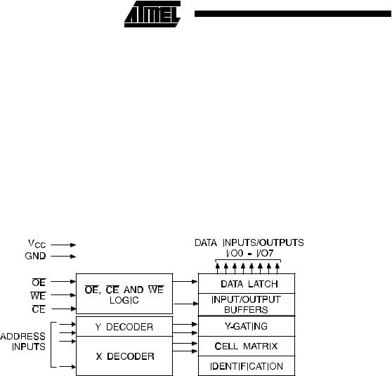
Block Diagram
Absolute Maximum Ratings*
Temperature Under Bias |
................. -55°C to +125°C |
||
Storage Temperature...................... |
-65°C to +150°C |
||
All Input Voltages |
|
||
(including NC Pins) |
|
||
with Respect to Ground ................... |
-0.6V to +6.25V |
||
All Output Voltages |
|
||
with Respect to Ground ............. |
- 0.6V to VCC + 0.6V |
||
|
|
|
|
Voltage on OE and A9 |
|
||
with Respect to Ground ................... |
-0.6V to +13.5V |
||
|
|
|
|
*NOTICE: Stresses beyond those listed under “Absolute Maximum Ratings” may cause permanent damage to the device. This is a stress rating only and functional operation of the device at these or any other conditions beyond those indicated in the operational sections of this specification is not implied. Exposure to absolute maximum rating conditions for extended periods may affect device reliability.
2-194 AT28C64/X 

Device Operation
READ: The AT28C64 is accessed like a Static RAM. When CE and OE are low and WE is high, the data stored at the memory location determined by the address pins is asserted on the outputs. The outputs are put in a high impedance state whenever CE or OE is high. This dual line control gives designers increased flexibility in preventing bus contention.
BYTE WRITE: Writing data into the AT28C64 is similar to writing into a Static RAM. A low pulse on the WE or CE input with OE high and CE or WE low (respectively) initiates a byte write. The address location is latched on the falling edge of WE (or CE); the new data is latched on the rising edge. Internally, the device performs a self-clear before write. Once a byte write has been started, it will automatically time itself to completion. Once a programming operation has been initiated and for the duration of tWC, a read operation will effectively be a polling operation.
FAST BYTE WRITE: The AT28C64E offers a byte write time of 200 μs maximum. This feature allows the entire device to be rewritten in 1.6 seconds.
READY/BUSY: Pin 1 is an open drain READY/BUSY output that can be used to detect the end of a write cycle. RDY/BUSY is actively pulled low during the write cycle and is released at the completion of the write. The open drain connection allows for OR-tying of several devices to the same RDY/BUSY line. Pin 1 is not connected for the AT28C64X.
AT28C64/X
DATA POLLING: The AT28C64 provides DATA POLLING to signal the completion of a write cycle. During a write cycle, an attempted read of the data being written results in the complement of that data for I/O7 (the other outputs are indeterminate). When the write cycle is finished, true data appears on all outputs.
WRITE PROTECTION: Inadvertent writes to the device are protected against in the following ways. (a) VCC sense— if V CC is below 3.8V (typical) the write function is inhibited. (b) VCC power on delay— once V CC h a s reached 3.8V the device will automatically time out 5 ms (typical) before allowing a byte write. (c) Write Inhibit— holding any one of OE low, CE high or WE high inhibits byte write cycles.
CHIP CLEAR: The contents of the entire memory of the AT28C64 may be set to the high state by the CHIP CLEAR operation. By setting CE low and OE to 12 volts, the chip is cleared when a 10 msec low pulse is applied to WE.
DEVICE IDENTIFICATION: A n e x t r a 32 - by t es of E2PROM memory are available to the user for device identification. By raising A9 to 12 ± 0.5V and using address locations 1FE0H to 1FFFH the additional bytes may be written to or read from in the same manner as the regular memory array.
2-195

DC and AC Operating Range
|
|
AT28C64-12 |
AT28C64-15 |
AT28C64-20 |
AT28C64-25 |
|
|
|
|
|
|
Operating |
Com. |
0°C - 70°C |
0°C - 70°C |
0°C - 70°C |
0°C - 70°C |
Temperature (Case) |
Ind. |
-40°C - 85°C |
-40°C - 85°C |
-40°C - 85°C |
-40°C - 85°C |
|
|||||
|
|
|
|
|
|
VCC Power Supply |
|
5V ± 10% |
5V ± 10% |
5V ± 10% |
5V ± 10% |
|
|
|
|
|
|
Operating Modes
|
|
|
|
|
|
|
|
|
Mode |
CE |
|
OE |
WE |
I/O |
|||
Read |
VIL |
|
VIL |
VIH |
DOUT |
|||
|
|
|
|
|
|
|
|
|
Write (2) |
VIL |
VIH |
VIL |
DIN |
||||
Standby/Write Inhibit |
VIH |
X (1) |
X |
High Z |
||||
Write Inhibit |
X |
|
X |
VIH |
|
|||
Write Inhibit |
X |
|
VIL |
X |
|
|||
Output Disable |
X |
|
VIH |
X |
High Z |
|||
|
|
|
|
|
|
|
|
|
Chip Erase |
VIL |
VH (3) |
VIL |
High Z |
||||
Notes: 1. X can be VIL or VIH. |
|
|
|
3. VH = 12.0V ± 0.5V. |
|
|
|
|
2. Refer to AC Programming Waveforms.
DC Characteristics
Symbol |
Parameter |
Condition |
|
Min Max |
Units |
||||
|
|
|
|
|
|
|
|
|
|
ILI |
Input Load Current |
VIN = 0V to VCC + 1V |
|
10 |
μA |
||||
|
|
|
|
|
|
|
|
|
|
ILO |
Output Leakage Current |
VI/O = 0V to VCC |
|
10 |
μA |
||||
|
|
|
|
|
|
|
|
|
|
|
|
|
|
|
|
|
|
μA |
|
ISB1 |
VCC Standby Current CMOS |
CE = VCC - 0.3V to VCC + 1.0V |
|
100 |
|||||
|
|
|
|
|
|
|
|
|
|
|
|
|
|
|
|
Com. |
2 |
mA |
|
ISB2 |
VCC Standby Current TTL |
CE = 2.0V to VCC + 1.0V |
|||||||
Ind. |
3 |
mA |
|||||||
|
|
|
|
|
|
||||
|
|
|
|
|
|
|
|
|
|
ICC |
VCC Active Current AC |
f = 5 MHz; IOUT = 0 mA |
Com. |
30 |
mA |
||||
CE = VIL |
Ind. |
45 |
mA |
||||||
|
|
||||||||
|
|
|
|
|
|
||||
|
|
|
|
|
|
|
|
|
|
VIL |
Input Low Voltage |
|
|
|
|
|
0.8 |
V |
|
|
|
|
|
|
|
|
|
|
|
VIH |
Input High Voltage |
|
|
|
|
|
2.0 |
V |
|
|
|
|
|
|
|
|
|
|
|
VOL |
Output Low Voltage |
IOL = 2.1 mA |
|
|
|
.45 |
V |
||
|
= 4.0 mA for RDY/BUSY |
|
|||||||
|
|
|
|
|
|
||||
|
|
|
|
|
|
|
|
|
|
VOH |
Output High Voltage |
IOH = -400 μA |
|
2.4 |
V |
||||
|
|
|
|
|
|
|
|
|
|
2-196 AT28C64/X 
 Loading...