

Page 1
¸SMJ100A Vector Signal Generator
Data sheet
Version
05.00
December
2007
Page 2

CONTENTS
Key features ..............................................................................................................................................................................................4
Baseband generator options ...................................................................................................................................................................5
Modulation ................................................................................................................................................................................................5
Possible modulation types ......................................................................................................................................................................5
Simultaneous modulation........................................................................................................................................................................5
RF characteristics ....................................................................................................................................................................................6
Frequency ...............................................................................................................................................................................................6
Frequency sweep....................................................................................................................................................................................6
Reference frequency...............................................................................................................................................................................6
Level .......................................................................................................................................................................................................7
Measured level data................................................................................................................................................................................8
Level sweep ............................................................................................................................................................................................9
Spectral purity .........................................................................................................................................................................................9
List mode ..............................................................................................................................................................................................10
Analog modulation .................................................................................................................................................................................11
Internal modulation generator ...............................................................................................................................................................11
Input for external modulation signals ....................................................................................................................................................11
Amplitude modulation ...........................................................................................................................................................................11
Wideband amplitude modulation...........................................................................................................................................................12
Pulse modulation ..................................................................................................................................................................................12
Frequency modulation (R&S®SMJ-B20 option) ....................................................................................................................................12
Phase modulation (R&S®SMJ-B20 option) ...........................................................................................................................................12
I/Q modulation ........................................................................................................................................................................................13
I/Q modulator ........................................................................................................................................................................................13
External wideband I/Q...........................................................................................................................................................................13
Internal baseband I/Q (with R&S®SMJ-B13 option) ..............................................................................................................................14
Differential I/Q output (R&S®SMJ-B16 option) ......................................................................................................................................16
Digital baseband output (R&S®SMJ-B18 option) ..................................................................................................................................17
I/Q baseband generator (R&S®SMJ-B9/-B10/-B11/-B50/-B51 option) – arbitrary waveform mode...................................................... 18
I/Q baseband generator (R&S®SMJ-B9/-B10/-B11 option) – realtime operation ..................................................................................20
Modulation uncertainty for main standards ...........................................................................................................................................24
Signal performance for digital standards ..............................................................................................................................................24
Digital standards (for the R&S®SMU-B9/-B10/-B11) ............................................................................................................................28
Digital standards with external PC software........................................................................................................................................28
Digital standards with R&S®WinIQSIM2™ (for the R&S®SMJ-B9/-B10/-B11/-B50/-B51 ARB) .........................................................29
Digital standards with R&S®WinIQSIM™ (for the R&S®SMJ-B9/-B10/-B11/-B50/-B51 ARB) ...........................................................29
R&S®SMJ100A Vector Signal Generator Version 05.00, December 2007
2
Page 3

Noise generation ....................................................................................................................................................................................30
Additive white Gaussian noise (AWGN, R&S®SMJ-K62 option)...........................................................................................................30
Other options ..........................................................................................................................................................................................31
BER measurement (R&S®SMJ-K80 option)..........................................................................................................................................31
BLER measurement (R&S®SMJ-K80 option)........................................................................................................................................31
General data............................................................................................................................................................................................32
Remote control......................................................................................................................................................................................32
Operating data ......................................................................................................................................................................................32
License information...............................................................................................................................................................................32
Ordering information..............................................................................................................................................................................33
Version 05.00, December 2007 R&S®SMJ100A Vector Signal Generator
3
Page 4

Key features
Intuitive operation
• Color display with 800 × 600 pixels (SVGA format)
• Intuitive user interface with graphical display of signal flow (block diagram)
• Graphical display of baseband signals through built-in transient recorder
• Context-sensitive help system
Outstanding signal quality
• I/Q modulator with 200 MHz RF bandwidth
• Very low SSB phase noise of typ. –133 dBc (f = 1 GHz, 20 kHz carrier offset, 1 Hz measurement bandwidth)
• Wideband noise of typ. –153 dBc (CW, f = 1 GHz, >10 MHz carrier offset, 1 Hz measurement bandwidth)
• Excellent ACLR performance of typ. +69 dB with 3GPP FDD (test model 1, 64 DPCH)
• Very high level repeatability of 0.05 dB
• High-stability reference oscillator as standard
Unrivaled flexibility
• Support of EUTRA/LTE signal generation
• Support of WiMAX IEEE 802.16-2004/Corr1-2005, 802.16e-2005, and WiBro
• Four code channels in realtime for 3GPP FDD, support of HSDPA and HSUPA
• Support of WLAN IEEE 802.11a, b, g and n
• Change of modulation from slot to slot for GSM/EDGE
• Baseband generator with universal coder for realtime signal generation
• Arbitrary waveform generator with 16 Msample, 64 Msample or 128 Msample and multisegment support
• Arbitrary waveform generator supported by R&S
Ideal for production
• Very short frequency and level setting times (<2 ms); only 450 µs in List mode
• Electronic attenuator with overvoltage protection up to 6 GHz over full level range
• Flexible high speed measurements with RF List mode and multisegment waveforms
®
WinIQSIM2TM and R&S®WinIQSIM
TM
simulation software
Connectivity
• Remote control via LAN (Gigabit Ethernet, VXI11) and GPIB
• Remote operation via Windows Remote Desktop or VNC
• User-selectable trigger and marker signals
• USB connectors for keyboard, mouse, and memory stick
• LXI class C compliance
R&S®SMJ100A Vector Signal Generator Version 05.00, December 2007
4
Page 5

Baseband generator options
The R&S®SMJ100A can be equipped with one of the following I/Q baseband generators:
®
SMJ-B9 Baseband Generator with ARB (128 Msample) and Digital Modulation (realtime)
R&S
R&S®SMJ-B10 Baseband Generator with ARB (64 Msample) and Digital Modulation (realtime)
R&S®SMJ-B11 Baseband Generator with ARB (16 Msample) and Digital Modulation (realtime)
R&S®SMJ-B50 Baseband Generator with ARB (64 Msample)
R&S®SMJ-B51 Baseband Generator with ARB (16 Msample)
The R&S
®
SMJ-B9/-B10/-B11 baseband generators include an arbitrary waveform generator and a realtime coder. If these baseband
generators are installed, the following software options can be added:
• Digital standards and modulation systems running on the instrument (R&S
• Digital standards with R&S
external PC
• Digital standards with R&S
®
• R&S
SMJ-K5/-K6/-K8 options
®
WinIQSIM2™ (R&S®SMJ-K240 to R&S®SMJ-K262 options); R&S®WinIQSIM2™ runs on an
®
WinIQSIM™ (R&S®SMJ-K11 to R&S®SMJ-K20 options); R&S®WinIQSIM™ runs on an external PC
®
SMJ-K40 to R&S®SMJ-K61 options)
The R&S
®
SMJ-B50/-B51 baseband generators include an arbitrary waveform generator. If these baseband generators are installed,
the following software options can be added:
• Digital standards with R&S
external PC
• Digital standards with R&S
®
• R&S
SMJ-K6 option
®
WinIQSIM2™ (R&S®SMJ-K240 to R&S®SMJ-K262 options); R&S®WinIQSIM2™ runs on an
®
WinIQSIM™ (R&S®SMJ-K11 to R&S®SMJ-K20 options); R&S®WinIQSIM™ runs on an external PC
Modulation
Possible modulation types
Amplitude modulation, frequency/phase modulation (optional), vector modulation, digital modulation via internal baseband section
(optional), pulse modulation, wideband amplitude modulation
Simultaneous modulation
AM FM φM Pulse BB-AM I/Q DM ARB
Amplitude modulation (AM) / + + + – – – –
Frequency modulation (FM) + / – + + + + +
Phase modulation (φM) + – / + + + + +
Pulse modulation + + + / + + + +
Broadband AM (BB-AM) – + + + / – – –
Vector modulation (I/Q) – + + + – / – –
Digital modulation (DM) – + + + – – / –
ARB – + + + – – – /
+ = compatible, – = not compatible, switch off each other
Version 05.00, December 2007 R&S®SMJ100A Vector Signal Generator
5
Page 6
RF characteristics
Frequency
Range
Resolution of setting 0.01 Hz
Resolution of synthesis standard, fundamental frequency range
Setting time1
Phase offset adjustable in 0.1° steps
Frequency sweep
Operating modes digital sweep in discrete steps automatic, step, single,
Sweep range full frequency range
underrange 100 kHz to <300 kHz
R&S®SMJ-B103 up to 3 GHz
®
R&S
SMJ-B106 up to 6 GHz
5 µHz
750 MHz to 1500 MHz
to within <1 × 10
7
−
for f > 200 MHz or
<124 Hz for f < 200 MHz,
with GUI update stopped
after IEC/IEEE bus delimiter <2 ms, typ. 1.5 ms
in ALC OFF MODE S&H <4 ms, typ. 2.5 ms
after trigger pulse in List mode <450 µs, typ. 300 µs
external single, external step,
manual or external trigger,
linear or logarithmic spacing
linear full frequency range Step width
logarithmic 0.01 % to 100 % per step
Reference frequency
Aging after 30 days of uninterrupted operation <1 × 10
Temperature effect in operating temperature range ±6 × 10
Warm-up time to nominal thermostat temperature ≤10 min
Output for internal reference signal
Input for external reference
Electronic tuning from input
AUX I/O
frequency (approx. sinewave) 10 MHz or external input frequency
level typ. 5 dBm
source impedance 50 Ω
frequency 5 MHz, 10 MHz or 13 MHz
maximum deviation 3 × 10
input level, limits ≥−6 dBm, ≤19 dBm
recommended 0 dBm to 19 dBm
input impedance 50 Ω
sensitivity typ. 1 × 10
input voltage –10 V to +10 V
input impedance 10 kΩ
9
−
/day, <1 × 10
8
−
6
−
8
−
/V to 3 × 10
7
−
/year
−
8
/V
1
Installation of software that is not authorized by Rohde & Schwarz for use on the R&S®SMJ100A or installation of antivirus software can deteriorate the
setting time performance.
R&S®SMJ100A Vector Signal Generator Version 05.00, December 2007
6
Page 7

Level
Setting range –145 dBm to +20 dBm
f ≤ 3 GHz +13 dBm (PEP)2 Maximum level
f > 3 GHz +11 dBm (PEP)
Resolution 0.01 dB
Level uncertainty
Additional uncertainty with
ALC OFF, S&H
Output impedance
VSWR in 50 Ω system
Setting time3
Back-feed (from ≥50 Ω source)
for levels >–120 dBm, attenuator mode
Auto, temperature range +18 °C to +28 °C
1 MHz ≤ f ≤ 3 GHz <0.5 dB
f > 3 GHz <0.9 dB
This function is needed only in some
special applications.
ALC state ON
f ≤ 3 GHz
f > 3 GHz
after IEC/IEEE bus delimiter,
to <0.1 dB deviation from final value,
with GUI update stopped,
temperature range +18 °C to +28 °C
ALC state ON <2 ms, typ. 1.5 ms
ALC state OFF <4 ms, typ. 2.5 ms
in List mode after trigger impulse to
<0.3 dB deviation from final value
with attenuator mode fixed, ALC state ON Uninterrupted level setting
setting range >20 dB
maximum permissible RF power in output
frequency range for f > 1 MHz
1 MHz ≤ f ≤ 3 GHz 50 W
f > 3 GHz 10 W
maximum permissible DC voltage 50 V
<0.2 dB
<1.6, typ. <1.4
<1.85, typ. <1.6
<450 µs, typ. 300 µs
2
PEP = peak envelope power.
3
Installation of software that is not authorized by Rohde & Schwarz for use on the R&S®SMJ100A or installation of antivirus software can deteriorate the
setting time performance.
Version 05.00, December 2007 R&S®SMJ100A Vector Signal Generator
7
Page 8
Measured level data
Measured level versus frequency
Level repeatability with random settings between measurements (upper diagram)
The lower diagram shows the temperature inside the instrument during the measurement
R&S®SMJ100A Vector Signal Generator Version 05.00, December 2007
8
Page 9

Level sweep
Operating modes digital sweep in discrete steps automatic, single, step,
external single, external step,
manual, or external trigger
Sweep range full level range
Step width logarithmic 0.1 dB to 20 dB per step
range 10 ms to 10 s Dwell time
resolution 0.1 ms
Spectral purity
Harmonics
Nonharmonics
Power supply and mechanically related
nonharmonics
Wideband noise
SSB phase noise
Residual FM
Residual AM rms value 20 Hz to 23 kHz <0.02 %
unmodulated
level <8 dBm <–30 dBc
level <13 dBm typ. <–30 dBc
level >–50 dBm, CW,
vector modulation (full-scale DC input),
>10 kHz offset from carrier and
outside the modulation spectrum
0.3 MHz ≤ f ≤ 200 MHz <–77 dBc
200 MHz < f ≤ 1500 MHz <–80 dBc
1500 MHz < f ≤ 3000 MHz <–74 dBc
f > 3000 MHz <–68 dBc
850 kHz offset from carrier and
outside the modulation spectrum
0.3 MHz ≤ f ≤ 200 MHz <–77 dBc
200 MHz < f ≤ 1500 MHz <–86 dBc
1500 MHz < f ≤ 3000 MHz <–80 dBc
f > 3000 MHz <–74 dBc
at RF = 1 GHz,
50 Hz to 10 kHz from carrier
1500 MHz < f ≤ 3000 MHz <–74 dBc Subharmonics
3000 MHz < f ≤ 6000 MHz <–50 dBc
carrier offset >10 MHz,
measurement bandwidth 1 Hz, CW
20 MHz ≤ f ≤ 200 MHz <–146 dBc (typ. –149 dBc)
200 MHz < f ≤ 1500 MHz <–150 dBc (typ. –153 dBc)
1.5 GHz < f ≤ 3 GHz <–148 dBc (typ. –151 dBc)
f > 3 GHz <–146 dBc (typ. –149 dBc)
vector modulation with full-scale DC input
20 MHz ≤ f ≤ 200 MHz <–140 dBc (typ. –143 dBc)
200 MHz < f ≤ 1500 MHz <–143 dBc (typ. –146 dBc)
1.5 GHz < f ≤ 3 GHz <–142 dBc (typ. –145 dBc)
f > 3 GHz <–140 dBc (typ. –143 dBc)
carrier offset 20 kHz, measurement
bandwidth 1 Hz, unmodulated
20 MHz ≤ f ≤ 200 MHz <–126 dBc (typ. –130 dBc)
f = 1 GHz <–129 dBc (typ. –133 dBc)
f = 2 GHz <–123 dBc (typ. –127 dBc)
f = 3 GHz <–119 dBc (typ. –123 dBc)
f = 4 GHz <–117 dBc (typ. –121 dBc)
f = 6 GHz <–113 dBc (typ. –117 dBc)
rms value at f = 1 GHz
300 Hz to 3 kHz <1 Hz
20 Hz to 23 kHz <4 Hz
<–70 dBc
Version 05.00, December 2007 R&S®SMJ100A Vector Signal Generator
9
Page 10
List mode
Frequency and level values can be stored in a list and set in an extremely short amount of time.
Operating modes automatic, single sweep, manual or
external trigger
Maximum number of channels 10000
Dwell time 1 ms to 1 s
Resolution 0.1 ms
Setting time after external trigger see frequency and level data
R&S®SMJ100A Vector Signal Generator Version 05.00, December 2007
10
Page 11
Analog modulation
Internal modulation generator
Frequency range 0.1 Hz to 1 MHz
Resolution of setting 0.1 Hz
Frequency uncertainty <0.012 Hz +
relative deviation of reference frequency
up to 100 kHz <0.1 dB Frequency response
up to 1 MHz <1 dB
Distortion up to 100 kHz at RL >200 Ω, level (Vp) 1 V <0.1 %
Output voltage
Output impedance 16 Ω
Frequency setting time to within <1 × 10
Sweep
Input for external modulation signals
Modulation input
EXT MOD
Vp at LF connector, RL >200 Ω 1 mV to 3 V
resolution 1 mV
setting uncertainty at 1 kHz <(1 % of reading + 1 mV)
7
−
stopped, after IEC/IEEE bus delimiter
, with GUI update
digital sweep in discrete steps
operating modes automatic, step, single,
sweep range full frequency range
linear step width full frequency range
logarithmic step width 0.01 % to 100 % per step
input impedance high (>100 kΩ), switchable to 50 Ω
input sensitivity (peak value for set
modulation depth or deviation)
absolute maximum rating 10 V
<3 ms
external single, external step,
manual or external trigger,
linear or logarithmic spacing
with R&S
1 V
®
SMJ-B20 option
Amplitude modulation
Operating modes internal, external AC/DC
Modulation depth At high levels, modulation is clipped if the
maximum PEP is reached.
Resolution 0.1 %
Setting uncertainty attenuator mode Auto,
AM distortion
Modulation frequency range DC, 20 Hz to 500 kHz
Modulation frequency response AC mode, 20 Hz to 500 kHz <1 dB
Incidental φM at AM m = 30 %, f
f
= 1 kHz and m <80 %
mod
PEP in specified range, attenuator mode
Auto
f ≤ 3 GHz, at f
m = 30 % <0.5 %
m = 80 % <0.8 %
f > 3 GHz, at f
m = 30 % <1 %
m = 80 % <1.6 %
= 1 kHz
mod
= 1 kHz
mod
= 1 kHz, peak value <0.1 rad
mod
0 % to 100 %
<(1 % of reading + 1 %)
Version 05.00, December 2007 R&S®SMJ100A Vector Signal Generator
11
Page 12
Wideband amplitude modulation
Operating modes modulation input I external DC
Modulation frequency response as with I/Q modulation –
external wideband I/Q
Input impedance 50 Ω
Input sensitivity peak voltage for 100 % AM 0.25 V
Pulse modulation
Operating modes external,
internal (duty cycle approx. 1:1)
ON/OFF ratio >70 dB
Rise/fall time 10 %/90 % of RF amplitude typ. 1 µs
Pulse repetition frequency 0 Hz to 100 kHz
Video crosstalk spectral line of fundamental of
100 kHz squarewave modulation
Modulation input
EXT MOD A/B
input level rising 1.7 V, falling typ. 1.1 V
input impedance >10 kΩ
polarity selectable
<−30 dBc
Frequency modulation (R&S®SMJ-B20 option)
Operating modes internal, external, internal + external,
AC/DC
FM/φM range multiplier
Maximum deviation rm × 10 MHz
Resolution <200 ppm, min. rm × 0.1 Hz
Setting uncertainty
FM distortion f
Carrier frequency offset at FM <0.2 % of set deviation
0.3 MHz ≤ f ≤ 200 MHz rm = 1
200 MHz < f ≤ 375 MHz rm = 0.25
375 MHz < f ≤ 750 MHz rm = 0.5
750 MHz < f ≤ 1500 MHz rm = 1
1500 MHz < f ≤ 3000 MHz rm = 2
f > 3000 MHz rm = 4
f
= 10 kHz,
mod
deviation ≤ half of maximum deviation
internal <(1.5 % of reading + 20 Hz)
external <(2.0 % of reading + 20 Hz)
= 10 kHz and 1 MHz deviation <0.1 %
mod
10 Hz to 100 kHz <0.5 dB Modulation frequency response
10 Hz to 10 MHz <3 dB
40 kHz deviation, f
f > 3 GHz <0.2 %
mod
= 1 kHz, f > 5 MHz <0.1 % Synchronous AM
Phase modulation (R&S®SMJ-B20 option)
Operating mode internal, external, internal + external,
High Deviation φM mode rm × 20.0 rad Maximum deviation
High Bandwidth φM mode rm × 1.0 rad
High Deviation φM mode <200 ppm, min. rm × 20 µrad Resolution
High Bandwidth φM mode <0.1 %, min. rm × 20 µrad
f
Setting uncertainty
φM distortion f
R&S®SMJ100A Vector Signal Generator Version 05.00, December 2007
12
= 10 kHz,
mod
deviation ≤ half of maximum deviation
internal <(1.5 % of reading + 0.01 rad)
external <(2.0 % of reading + 0.01 rad)
= 10 kHz, half of maximum deviation <0.2 %, typ. 0.1 %
mod
High Deviation, 10 Hz to 500 kHz <1 dB Modulation frequency response
High Bandwidth, 10 Hz to 10 MHz <3 dB
AC/DC, High Bandwidth, High Deviation
Page 13
I/Q modulation
I/Q modulator
Operating modes external wideband I/Q,
I/Q impairments
I offset, Q offset
setting range −10 % to +10 %
resolution 0.01 %
gain imbalance
setting range −1.0 dB to +1.0 dB
resolution 0.001 dB
quadrature offset
setting range −10° to +10°
resolution 0.01°
I/Q swap I and Q signals swapped ON/OFF
External wideband I/Q
I/Q inputs
Modulation frequency range I/Q wideband ON 100 MHz
Carrier leakage without input signal, referenced to full-
Error vector
5
4
3
Delta / dB
2
input impedance 50 Ω
VSWR up to 50 MHz <1.2
input voltage for full-scale input
minimum input voltage for ALC state ON 0.1 V
4
scale input
measured with 16QAM, root cosine filter,
α = 0.5, symbol rate 10 kHz
rms value
f ≤ 200 MHz <0.3 %
f > 200 MHz <(0.2 % + 0.1 % × f/GHz)
peak value
f ≤ 200 MHz <0.6 %
f > 200 MHz <(0.4 % + 0.2 % × f/GHz)
internal baseband I/Q
22
+= 0.5 V
VV
i
q
<
−55 dBc, typ. <−65 dBc
RF 850 MHz
RF 1900 MHz
RF 2200 MHz
1
0
–1
– 2
– 3
– 4
– 5
– 100 100060– 20– 60 20 40 80– 80 – 40
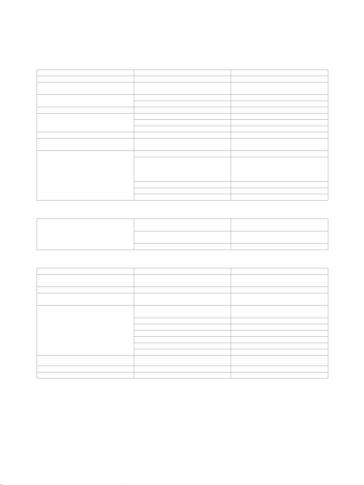
Frequency offset from carrier / MHz
Measured frequency response of external wideband I/Q modulation
4
Value applies after 1 hour warm-up and recalibration for 4 hours of operation and temperature variations of less than +5 °C.
Version 05.00, December 2007 R&S®SMJ100A Vector Signal Generator
13
Page 14

Internal baseband I/Q (with R&S®SMJ-B13 option)
The R&S®SMJ-B13 converts the internal digital baseband signals of the R&S®SMJ-B9/-B10/-B11/-B50/-B51 into analog signals for
driving the I/Q modulator. It also generates the analog I/Q output signals.
D/A converter
data rate 100 MHz
resolution 16 bit
sampling rate 400 MHz (internal interpolation × 4)
Aliasing filter
with amplitude, group delay and
Si correction
bandwidth, roll-off to −0.1 dB 40 MHz
D/A converter interpolation spectra
up to 10 MHz <−80 dBc
I/Q impairment
up to 40 MHz <
carrier leakage
setting range −10 % to +10 %
−73 dBc
resolution 0.01 %
I ≠ Q (imbalance)
setting range −1 dB to +1 dB
resolution 0.001 dB
quadrature offset
setting range −10° to +10°
resolution 0.01°
RF frequency response for entire
instrument in modulation bandwidth
I/Q wideband ON, optimize internal I/Q
impairments for RF output ON
up to 10 MHz <1.5 dB, typ 0.7 dB
up to 40 MHz <4.5 dB, typ. 2.0 dB
up to 10 MHz >44 dB, typ. 50 dB Suppression of image sideband for entire
up to 40 MHz >34 dB, typ. 44 dB
instrument in modulation bandwidth
5
Carrier leakage5 referenced to full-scale input <−55 dBc, typ. <−65 dBc
Additional level uncertainty referenced to
CW
measured at 0 dBm with 16QAM, root
cosine filter,
α = 0.5, symbol rate 10 kHz
<0.2 dB
I/Q outputs
Output impedance 50 Ω
Output voltage EMF (output voltage depends on set
1 V (Vp)
modulation signal)
Offset EMF <1 mV
Frequency response6
at RL = 50 Ω
magnitude
up to 10 MHz typ. 0.02 dB
up to 40 MHz typ. 0.03 dB
nonlinear phase
up to 10 MHz typ. 0.1°
up to 30 MHz typ. 0.2°
I/Q balance6
at RL = 50 Ω
magnitude
up to 10 MHz typ. 0.01 dB
up to 40 MHz typ. 0.02 dB
nonlinear phase
up to 10 MHz typ. 0.1°
up to 30 MHz typ. 0.2°
Spectral purity
at RL = 50 Ω
SFDR (sine)
up to 2 MHz >70 dB
up to 20 MHz typ. 60 dB
phase noise
10 MHz sinewave at 20 kHz offset typ. −150 dBc
wideband noise
10 MHz sinewave at 1 MHz offset typ. −155 dBc
5
Value applies after 1 hour warm-up time and recalibration for 4 hours of operation and temperature variations of less than +5 °C.
6
Optimize internal I/Q impairments for RF output switched OFF.
R&S®SMJ100A Vector Signal Generator Version 05.00, December 2007
14
Page 15
Frequency response of I/Q outputs
SFDR of I/Q outputs
Version 05.00, December 2007 R&S®SMJ100A Vector Signal Generator
15
Page 16

Differential I/Q output (R&S®SMJ-B16 option)
Additional specifications for I/Q outputs with R&S®SMJ-B16 option
Output impedance
Single-ended 50 Ω
Differential 100 Ω
Output voltage output voltage depends on set modulation
signal
Single-ended EMF 0.02 V to 2 V (Vp)
Resolution 1 mV
Differential EMF 0.04 V to 4 V (Vpp)
Resolution 2 mV
Bias voltage (single-ended and differential) EMF –3.6 V to +3.6 V
Resolution 2 mV
Uncertainty 1 % + 4 mV
Offset voltage
Differential EMF –300 mV to +300 mV
Resolution 0.2 mV
Uncertainty 1 % + 0.1 % × bias voltage + 1 mV
Differential signal balance
Frequency response7
at RL = 50 Ω, output voltage >0.5 V (Vp)
magnitude
up to 10 MHz <0.2 dB, typ. 0.05 dB
up to 40 MHz typ 0.2 dB
at RL = 50 Ω, output voltage >0.5 V (Vp)
magnitude
up to 10 MHz typ. 0.02 dB
up to 40 MHz typ. 0.03 dB
nonlinear phase
up to 10 MHz typ. 0.1°
up to 30 MHz typ. 0.2°
7
Optimize internal I/Q impairments for RF output switched OFF.
R&S®SMJ100A Vector Signal Generator Version 05.00, December 2007
16
Page 17

Digital baseband output (R&S®SMJ-B18 option)
The R&S®SMJ-B18 option makes digital I/Q signals available on the rear panel of the instrument. The digital I/Q output can be used
for the lossless connection of the R&S
baseband signal generator and fading simulator).
®
SMJ100A to the digital I/Q input of other Rohde & Schwarz instruments (e.g. R&S®AMU200A
Interface standard in line with Rohde & Schwarz TVR290,
I/Q data and control signals, data and
interface clock
level LVDS
connector 26-pin MDR
data rate 30 MHz to 100 MHz with 1 MHz resolution,
81.6 MHz
I/Q sample rate
With source ‘user-defined’, the sample rate must be entered via the parameter ‘sample
rate’, no I/Q data clock being necessary. With source ‘digital I/Q out’ or ‘digital I/Q in’,
the sample rate will be estimated on the basis of the applied I/Q data clock.
source user-defined, digital I/Q out, digital I/Q in
sample rate 400 Hz to 100 MHz
max. sample rate limited by actual
interface data rate
resolution (user-defined) 0.001 Hz
frequency uncertainty (user-defined) < 5 × 10
–14
I/Q data resolution 18 bit
logic format two's complement
physical signal level
setting range 0 to –60 dBFS
resolution 0.01 dBFS
bandwidth
sample rate = 100 MHz (no
interpolation, user-defined)
40 MHz
sample rate <100 MHz (interpolation) 0.31 × sample rate
Control signals markers 4
data valid valid samples marked in data stream
Version 05.00, December 2007 R&S®SMJ100A Vector Signal Generator
17
Page 18

I/Q baseband generator (R&S®SMJ-B9/-B10/-B11/-B50/-B51 option) –
arbitrary waveform mode
The R&S®SMJ-B13 baseband main module must be installed.
Waveform memory
Multisegment waveform
Multicarrier waveform
Clock generation
Interpolation
output memory
waveform length with the R&S®SMJ-B9 128 sample to 128 Msample in
one-sample steps
waveform length with the
®
SMJ-B10/-B50
R&S
waveform length with the
®
SMJ-B11/-B51
R&S
128 sample to 64 Msample in one-sample
steps
128 sample to 16 Msample in one-sample
steps
resolution 16 bit
loading time 10 Msample 15 s
nonvolatile memory hard disk
number of segments max. 100 segments
changeover modes GUI, remote control, external trigger
extended trigger modes
changeover time
same segment, next segment, next
segment seamless
typ. 5 µs at 50 MHz clock rate
(external trigger, without clock change)
seamless changeover output up to end of current segment,
followed by changeover to next segment
number of carriers max. 32
total RF bandwidth max. 80 MHz
crest factor modes maximize, minimize, off
signal period modes longest file, shortest file, user (max. 1 s)
single carrier gain –80 dB to 0 dB
single carrier start phase 0° to 360°
single carrier delay 0 s to 1 s
clock rate 400 Hz to 100 MHz
resolution 0.001 Hz
operating mode internal, external
frequency uncertainty (internal) <5 × 10
14
−
× clock rate +
uncertainty of reference frequency
The sampling rate of the waveform is
automatically interpolated to the internal
100 MHz data rate.
bandwidth
clock rate = 100 MHz (no interpolation),
40 MHz
roll-off to –0.1 dB
clock rate
≤100 MHz, drop to −0.1 dB 0.31 × clock rate
R&S®SMJ100A Vector Signal Generator Version 05.00, December 2007
18
Page 19

Triggering
In internal clock mode, a trigger event
restarts the clock generation. The clock
phase is then synchronous with the trigger
(with a certain timing uncertainty).
In external clock mode, the trigger event is
synchronized to the symbol clock.
operating mode internal, external
modes Auto, Retrig, Armed Auto, Armed Retrig
setting uncertainty for clock phase related
<18 ns
to trigger in internal clock mode
external trigger delay
setting range 0 sample to (216 – 1) sample
resolution
internal clock mode 0.01 sample
external clock mode 1 sample
setting uncertainty <5 ns
external trigger inhibit
setting range 0 sample to (226 – 1) sample
resolution 1 sample
external trigger pulse width >15 ns
external trigger frequency <0.02 × sampling rate
Marker outputs
number 4
level LVTTL
operating modes unchanged, restart, pulse, pattern, ratio
marker delay
setting range 0 sample to (waveform length − 1) sample
setting range without recalculation 0 sample to 2000 sample
resolution of setting 0.001 sample
setting uncertainty <10 ns
Operation with R&S®WinIQSIM2™: As of version 2.04, the software supports I/Q data download and control of the
®
SMJ-B9/-B10/-B11/-B50/-B51.
R&S
Operation with R&S®WinIQSIM™: As of version 4.50, the software supports I/Q data download and control of the
®
SMJ-B9/-B10/-B11/-B50/-B51.
R&S
Version 05.00, December 2007 R&S®SMJ100A Vector Signal Generator
19
Page 20

I/Q baseband generator (R&S®SMJ-B9/-B10/-B11 option) – realtime operation
The R&S®SMJ-B13 baseband main module must be installed.
Types of modulation
ASK
modulation index 0 % to 100 %
resolution 0.1 %
FSK 2FSK, 4FSK, MSK
deviation 0.1 to 1.5 × f
maximum 10 MHz
resolution <0.1 Hz
setting uncertainty <0.5 %
variable FSK 4FSK, 8FSK, 16FSK
deviations –1.5 × f
maximum 10 MHz
resolution <0.1 Hz
PSK BPSK, QPSK, QPSK 45° offset, OQPSK,
QAM 16QAM, 32QAM, 64QAM, 256QAM,
Coding Not all coding methods can be used with
every type of modulation.
Baseband filter
Any filter can be used with any type of
modulation. The bandwidth of the
modulation signal is max. 25 MHz; the
signal is clipped if the bandwidth is
exceeded.
cosine, root cosine
filter parameter α 0.05 to 1.00
Gaussian
filter parameter B × T 0.15 to 2.50
cdmaOne, cdmaOne + equalizer
cdmaOne 705 kHz,
cdmaOne 705 kHz + equalizer
CDMA2000
®
3x
APCO25 C4FM
rectangular
split phase
filter parameter B × T 0.15 to 2.5
resolution of filter parameter 0.01
sym
to +1.5 × f
sym
sym
π/4-QPSK, π/2-DBPSK, π/4-DQPSK,
π/8-D8PSK, 8PSK, 8PSK EDGE
1024QAM
OOFF, Differential, Diff. Phase,
Diff. + Gray, Gray, GSM, NADC, PDC,
PHS, TETRA, APCO25 (PSK), PWT,
TFTS, INMARSAT, VDL, EDGE,
APCO25(FSK), ICO, CDMA2000
® 8
,
WCDMA
8
CDMA2000® is a registered trademark of the Telecommunications Industry Association (TIA – USA).
R&S®SMJ100A Vector Signal Generator Version 05.00, December 2007
20
Page 21

Symbol rate
Frequency offset
Data sources
If an external clock is used, the applied
data rate may deviate from the set clock
±2 %. The external clock can be
rate by
used for internal and external data.
operating mode internal, external
setting range
ASK, PSK, QAM 400 Hz to 25 MHz
FSK 400 Hz to 15 MHz
resolution 0.001 Hz
frequency uncertainty (internal)
–14
<5 × 10
× symbol rate + reference
frequency uncertainty
external clock symbol, K × symbol, bit clock
clock divider K 1 to 64
external clock rate max. 100 MHz
With the aid of the frequency offset, the
center frequency of the modulation signal
in the baseband can be shifted. The
restrictions caused by the modulation
bandwidth apply.
setting range −40 MHz to +40 MHz
resolution 0.01 Hz
frequency uncertainty <5 × 10
10
−
× frequency offset + reference
frequency error
internal
all 0, all 1
PRBS
sequence length 9, 11, 15, 16, 20, 21, 23
pattern
length 1 bit to 64 bit
data lists
output memory of the R&S®SMJ-B9 8 bit to 4 Gbit
output memory of the R&S®SMJ-B10 8 bit to 2 Gbit
output memory of the R&S®SMJ-B11 8 bit to 512 Mbit
nonvolatile memory hard disk
external
In the case of serial transmission, the
symbol strobe marks the LSB of the
symbol, and the maximum symbol rate is
limited by the data rate of the interface.
serial
word width 1 bit to 10 bit
bit rate max. 60 MHz
parallel
word width 1 bit to 10 bit
symbol rate max. 25 MHz
Version 05.00, December 2007 R&S®SMJ100A Vector Signal Generator
21
Page 22

Triggering
In internal clock mode, a trigger event
restarts the clock generation. The clock
phase is then synchronous with the trigger
(with a certain timing uncertainty).
In external clock mode, the trigger event is
synchronized to the symbol clock.
operating mode internal, external
modes Auto, Retrig, Armed Auto, Armed Retrig
setting uncertainty for clock phase related
<18 ns
to trigger in internal clock mode
external trigger delay
setting range 0 sample to (216 – 1) sample
resolution
internal clock mode 0.01 sample
external clock mode 1 sample
setting uncertainty <5 ns
external trigger inhibit 0 sample to (226 – 1) sample
setting range
resolution 1 sample
external trigger pulse width >15 ns
external trigger frequency <0.02 × sampling rate
Marker outputs
number 4
level LVTTL
operating modes control list, restart, pulse, pattern, ratio
marker delay (in sample)
setting range 0 to (224 – 1)
setting range without recalculation 0 to 2000
resolution of setting 0.001
setting uncertainty <10 ns
Level reduction
Internal or external via LEVATT input. The
signal switches between nominal and
reduced level (without edge shaping). If an
internal LEVATT signal is used, the
connector is used as an output.
setting range 0 dB to 60 dB
additional level error in case of reduction
up to 30 dB <1 dB
up to 50 dB <3 dB
Burst
Internal or external via BURST input. The
signal triggers the beginning of a power
ramp. The positive edge starts power
ramping from blank to full level, the
negative edge ramping in the opposite
direction from full level to blanking. If an
internal BURST GATE signal is applied,
the connector is used as an output.
operating range max. 5 MHz
rise/fall time
setting range 0.5 symbol to 16 symbol
resolution 0.1 symbol
ramp shape cosine, linear
Trigger/clock/data inputs
The input impedance and trigger threshold
can be set separately for the trigger and
the clock/data inputs.
input impedance 1 kΩ, 50 Ω
trigger threshold
setting range 0.00 V to 2.50 V
resolution 0.01 V
Clock/data outputs level LVTTL
R&S®SMJ100A Vector Signal Generator Version 05.00, December 2007
22
Page 23

Modulation errors
Deviation error with 2FSK, 4FSK
Phase error with MSK
EVM with QPSK, OQPSK, π/4-DQPSK,
8PSK, 16QAM, 32QAM, 64QAM
modulation, filter, symbol rate, and coding
in line with standard
standards Bluetooth
Predefined settings
® 9
EDGE, NADC, PDC, PHS, TETRA,
WCDMA 3GPP, TD-SCDMA, CDMA2000
Forward, CDMA2000
Worldspace
deviation 0.2 to 0.7 × symbol rate
Gaussian filter with B × T = 0.2 to 0.7
symbol rate up to 2 MHz <1.2 %, typ. 0.25 %
symbol rate up to 10 MHz typ. 0.75 %
Gaussian filter with B × T = 0.2 to 0.7
bit rate up to 2 MHz <0.4°, typ. 0.15°
bit rate up to 10 MHz typ. 0.3°
cosine, root cosine filter with α = 0.2 to 0.7
symbol rate up to 5 MHz <0.8 %, typ. 0.2 %
symbol rate up to 20 MHz typ. 0.7 %
, DECT, ETC, GSM, GSM
®
Reverse,
®
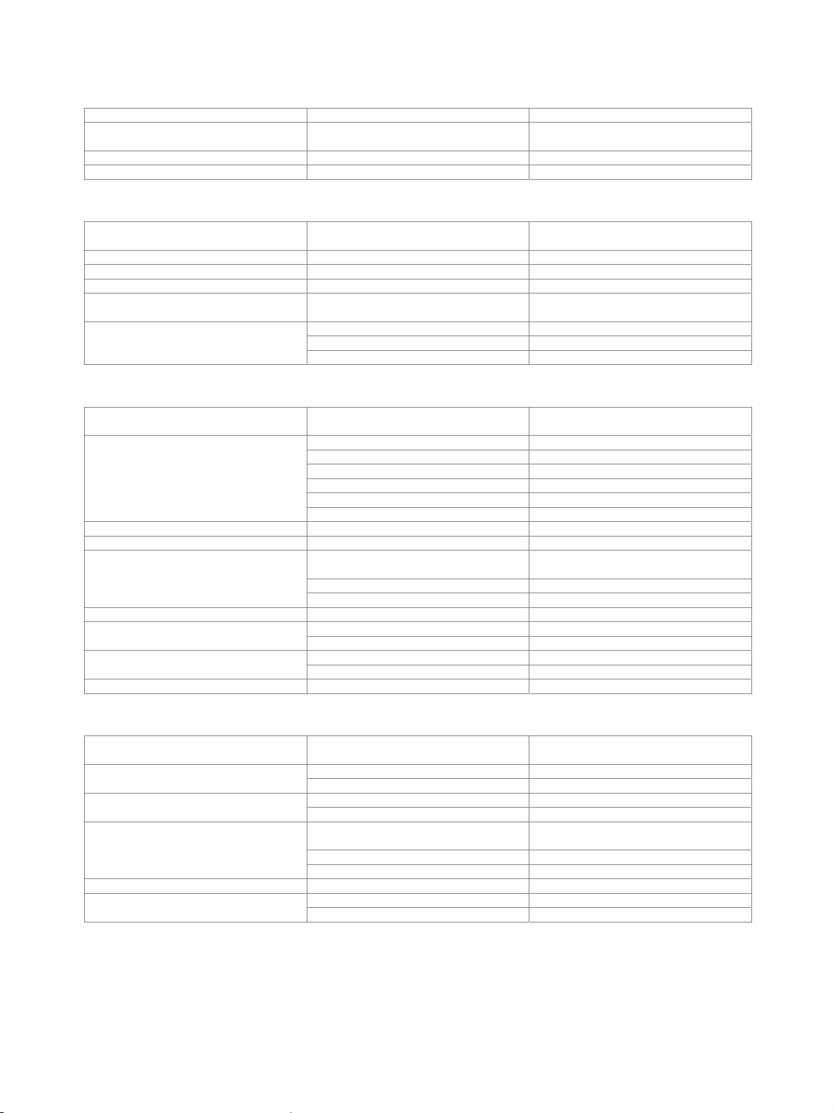
Measured EVM versus symbol rate
9
The Bluetooth® word mark and logos are owned by the Bluetooth SIG, Inc. and any use of such marks by Rohde & Schwarz is under license.
Version 05.00, December 2007 R&S®SMJ100A Vector Signal Generator
23
Page 24

Modulation uncertainty for main standards
Typical values
Standard GSM EDGE WCDMA
3GPP
(1DPCH)
Frequency
in MHz
EVM in % – 0.2 0.3 0.2 – 0.2 0.2 0.2 0.4
Phase error in ° 0.15 – – – – – – – –
Deviation error
in kHz
Channel spacing 200 kHz 200 kHz 5 MHz 1.25 MHz 1.728 MHz 25 kHz 30 kHz 25 kHz –
Adjacent channel power ratio (ACPR) in dB
In adjacent
channel
In alternate
channel
In 2nd alternate
channel
400 to
2000
– – – – 0.5 – – – –
−37 −38 −72 −80
−71 −71 −76 −93
−85 −85 – – – – – – −66
400 to
2000
1800 to
2200
cdmaOne
Reverse
800 to 900 824 to 894 810 to 956 2400 to
1850 to
2000
offset
750 kHz,
bandwidth
30 kHz
offset
1.98 MHz,
bandwidth
30 kHz
DECT TETRA NADC PDC IEEE
802.11a
1880 to 1990 380 to
480
1850 to
2000
– −74 −34 −71 −42
– −77 −78 −77 −64
1429 to
1501
2485
5150 to
5825
at 11 MHz
at 20 MHz
at 30 MHz
Signal performance for digital standards
GSM/EDGE with R&S
Burst ON/OFF ratio >100 dB
Phase error
Error vector magnitude 8PSK EDGE, Gaussian linearized filter,
Power density spectrum
MSK, Gaussian filter B × T = 0.3
rms
values measured with 30 kHz resolution
bandwidth, referenced to level in band
center without power ramping
level ≤10.5 dBm
®
SMJ-K40 option
rms <0.4°, typ. 0.15°
peak <1.2°, typ. 0.4°
<0.5 %, typ. 0.2 %
frequency 400 MHz to 2 GHz
200 kHz offset <–34 dB, typ. –37 dB
400 kHz offset <–68 dB, typ. –71 dB
600 kHz offset <–80 dB, typ. –85 dB
R&S®SMJ100A Vector Signal Generator Version 05.00, December 2007
24
Page 25

3GPP FDD with R&S
®
SMJ-K42 option
Error vector magnitude 1 DPCH, rms <0.8 %, typ. 0.3 %
Adjacent channel leakage ratio (ACLR)
test model 1, 64 DPCHs
level ≤10.5 dBm PEP
frequency 1800 MHz to 2200 MHz
offset 5 MHz >66 dB, typ. 69 dB
offset 10 MHz >68 dB, typ. 71 dB
ACLR (typical values) for 3GPP test model 1, 64 DPCH
ACLR (typical values) for a 3GPP four-carrier signal with test model 1, 64 DPCH on each carrier
Version 05.00, December 2007 R&S®SMJ100A Vector Signal Generator
25
Page 26
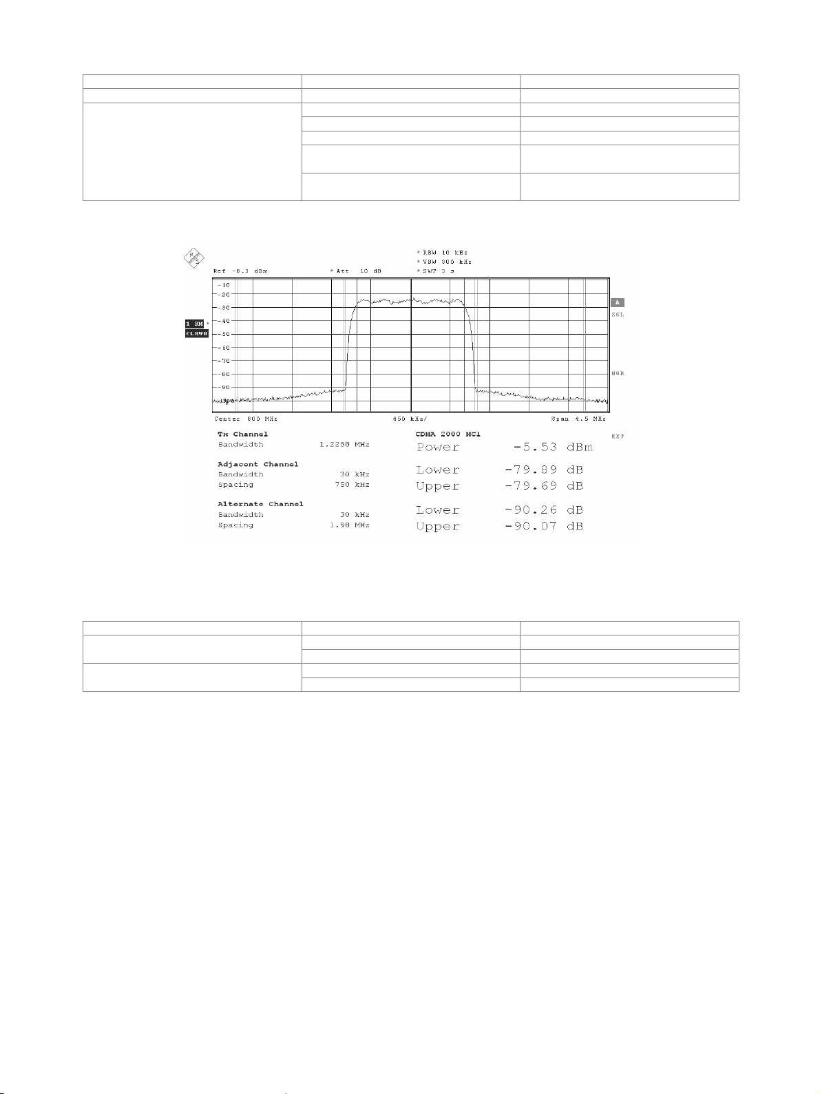
CDMA2000
®
with R&S
®
SMJ-K46 option
Error vector magnitude (EVM) F-PICH, F-SYNC, and one F-FCH, rms <0.8 %, typ. 0.3 %
Adjacent channel leakage ratio (ACLR)
F-PICH, F-SYNC, and one F-FCH
level ≤10.5 dBm PEP
carrier frequency 800 MHz
channel spacing 0.75 MHz
(bandwidth 30 kHz)
channel spacing 1.98 MHz
(bandwidth 30 kHz)
typ. 79 dB
typ. 90 dB
ACLR (typical values) for a CDMA2000
Multicarrier CW with R&S
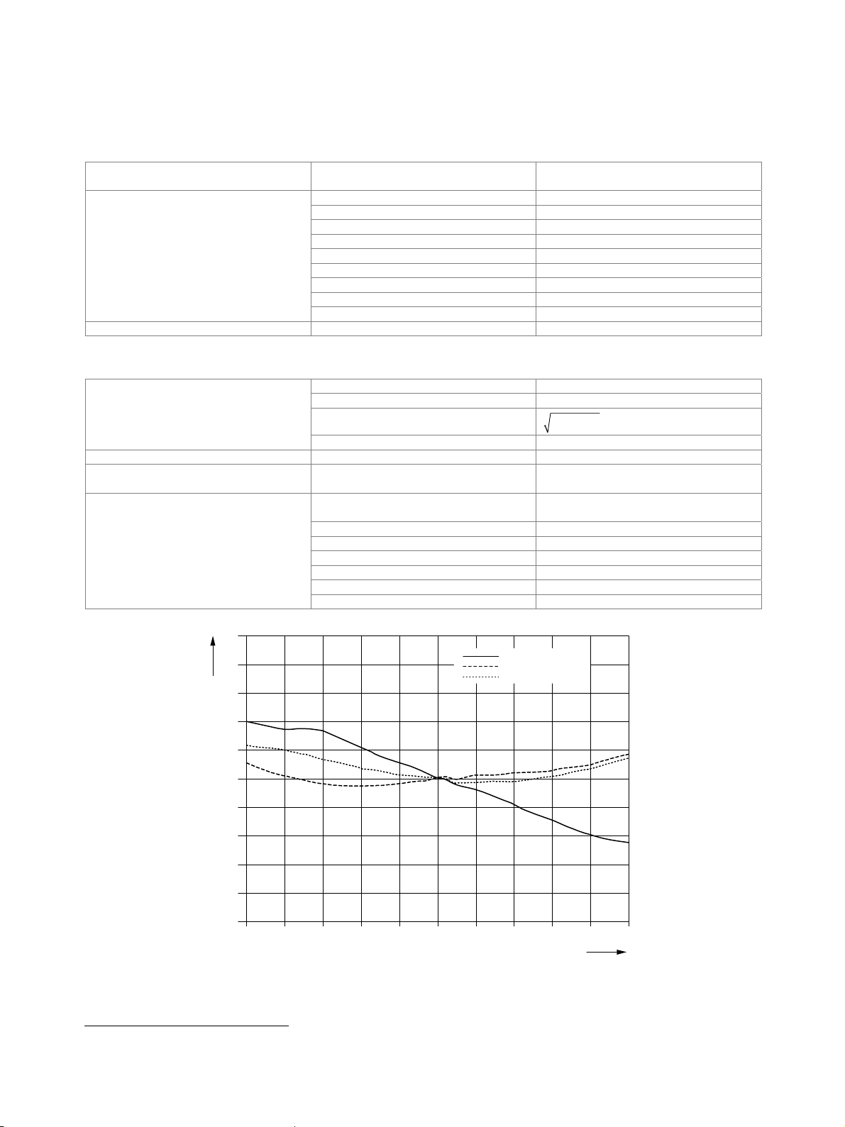
up to 10 MHz <1.5 dB, typ 0.7 dB RF frequency response
up to 40 MHz <4.5 dB, typ. 2.0 dB
up to 10 MHz >50 dB, typ. 56 dB Suppression of unwanted carriers
up to 40 MHz >40 dB, typ. 50 dB
®
1x signal consisting of F-PICH, F-SYNC, and one F-FCH
®
SMJ-K61 option
R&S®SMJ100A Vector Signal Generator Version 05.00, December 2007
26
Page 27
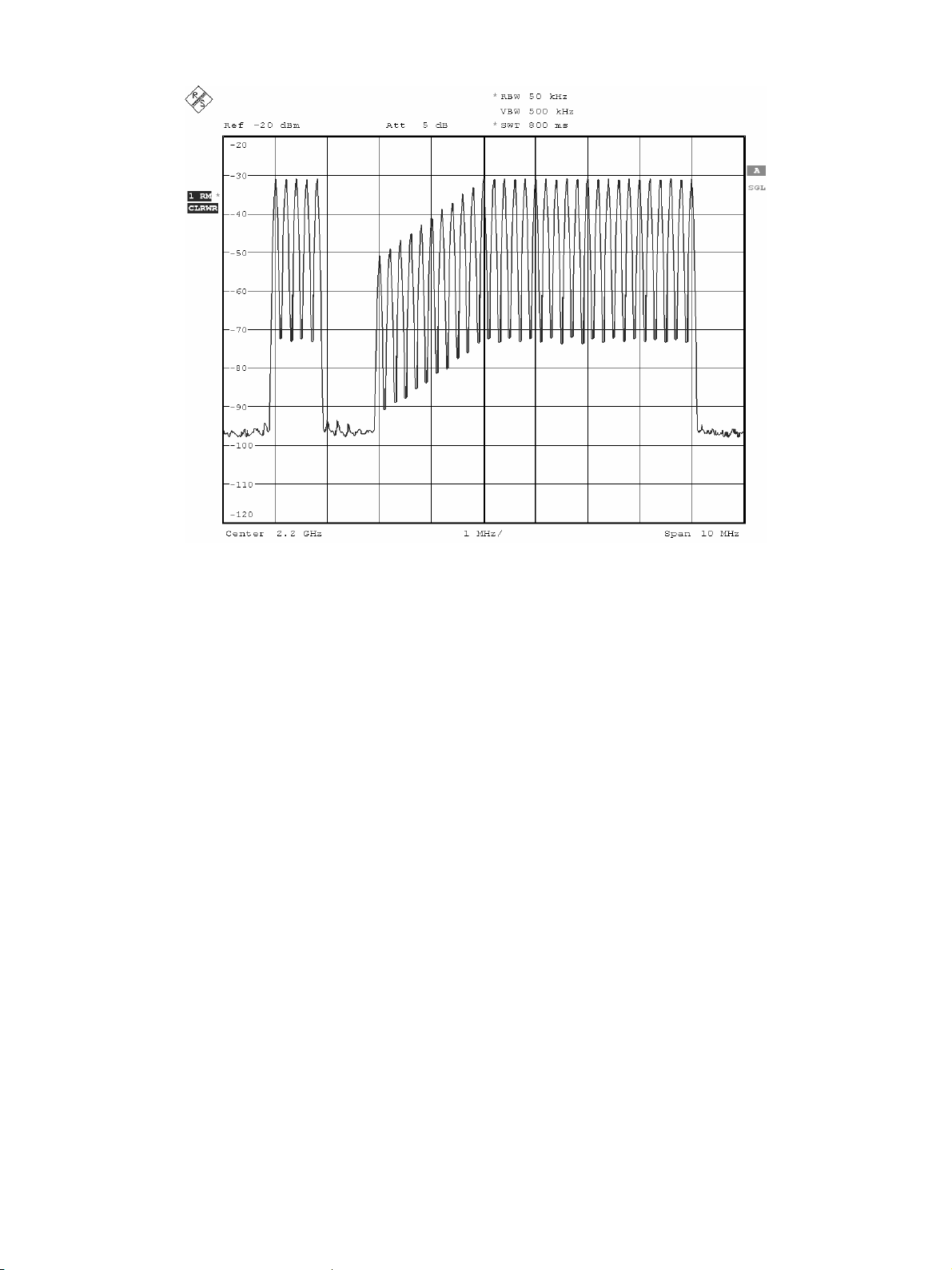
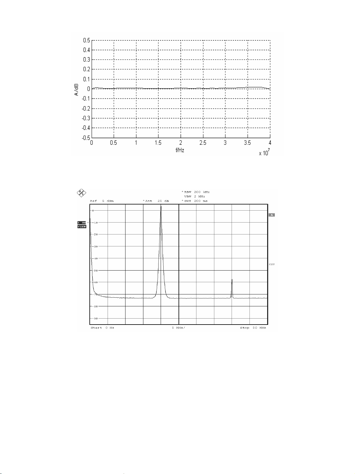
Example of multicarrier CW, with different carrier powers and some carriers switched off in the left half of the spectrum
Version 05.00, December 2007 R&S®SMJ100A Vector Signal Generator
27
Page 28

Digital standards (for the R&S®SMJ-B9/-B10/-B11)
An R&S®SMJ-B9, R&S®SMJ-B10, or R&S®SMJ-B11 I/Q baseband generator is required. The specified data applies together with the
parameters of the respective standard. The entire frequency range as well as filter parameters and symbol rates can be set by the
user.
GSM/EDGE digital standard R&S
3GPP FDD digital standard R&S®SMJ-K42 option
3GPP FDD enhanced BS/MS tests
including HSDPA
GPS digital standard R&S®SMJ-K44 option
3GPP FDD enhanced BS/MS tests
including HSUPA
CDMA2000® digital standard R&S®SMJ-K46 option
1xEV-DO digital standard R&S®SMJ-K47 option
IEEE 802.11a/b/g digital standard R&S®SMJ-K48 option
IEEE 802.16 WiMAX digital standard
including IEEE 802.16e
TD-SCDMA (3GPP TDD LCR) digital
standard
TD-SCDMA (3GPP TDD LCR) enhanced
BS/MS tests including HSDPA
DVB-H digital standard R&S®SMJ-K52 option
DAB / T-DMB digital standard R&S®SMJ-K53 option
IEEE 802.11n digital standard R&S®SMJ-K54 option
EUTRA/LTE digital standard R&S®SMJ-K55 option
XM RADIO digital standard R&S®SMJ-K56 option
Multicarrier CW signal generation R&S®SMJ-K61 option
®
SMJ-K40 option
R&S®SMJ-K43 option
R&S®SMJ-K45 option
R&S®SMJ-K49 option
R&S®SMJ-K50 option
R&S®SMJ-K51 option
The options are described in the Digital Standards data sheet (PD 5213.9434.22).
Digital standards with external PC software
An I/Q baseband generator must be installed. R&S®SMJ-K5 and -K8 require the R&S®SMJ-B9, -B10, or -B11. R&S®SMJ-K6 can be
used with theR&S
Bluetooth
software)
Pulse sequencer (external PC software) R&S®SMJ-K6 option
TETRA digital standard (external PC
software)
The options are described in the Digital Standards data sheet (PD 5213.9434.22).
®
SMJ-B9, -B10, -B11, -B50 or -B51.
®
digital standard (external PC
R&S®SMJ-K5 option
R&S®SMJ-K8 option
R&S®SMJ100A Vector Signal Generator Version 05.00, December 2007
28
Page 29
Digital standards with R&S®WinIQSIM2™
®
(for the R&S
GSM/EDGE digital standard R&S
3GPP FDD digital standard R&S®SMJ-K242 option
3GPP FDD enhanced BS/MS tests
including HSDPA
GPS digital standard R&S®SMJ-K244 option
3GPP FDD enhanced BS/MS tests
including HSUPA
CDMA2000® digital standard R&S®SMJ-K246 option
1 x EV-DO digital standard R&S®SMJ-K247 option
IEEE 802.11a/b/g digital standard R&S®SMJ-K248 option
IEEE 802.16 WiMAX digital standard
including IEEE 802.16e
TD-SCDMA (3GPP TDD LCR) digital
standard
TD-SCDMA (3GPP TDD LCR) enhanced
BS/MS tests including HSDPA
DVB-H digital standard R&S®SMJ-K252 option
IEEE 802.11n digital standard R&S®SMJ-K254 option
EUTRA/LTE digital standard R&S®SMJ-K255 option
XM RADIO digital standard R&S®SMJ-K256 option
Multicarrier CW signal generation R&S®SMJ-K261 option
Additive white Gaussian noise (AWGN) R&S®SMJ-K262 option
The options are described in the R&S
SMJ-B9/-B10/-B11/-B50/-B51 ARB)
®
SMJ-K240 option
R&S®SMJ-K243 option
R&S®SMJ-K245 option
R&S®SMJ-K249 option
R&S®SMJ-K250 option
R&S®SMJ-K251 option
®
WinIQSIM2™ data sheet (PD 5213.7460.22).
Digital standards with R&S®WinIQSIM™
®
(for the R&S
IS-95 digital standard R&S
CDMA2000® digital standard R&S®SMJ-K12 option
3GPP TDD HDR digital standard R&S®SMJ-K13 option
3GPP TDD LDR digital standard
(TD-SCDMA)
OFDM with R&S®WinIQOFDM R&S®SMJ-K15 option
1xEV-DO (Rev. 0) digital standard R&S®SMJ-K17 option
IEEE 802.11a/b/g digital standard R&S®SMJ-K19 option
3GPP FDD digital standard including
HSDPA
The options are described in the R&S
SMJ-B9/-B10/-B11/-B50/-B51 ARB)
®
SMJ-K11 option
R&S®SMJ-K14 option
R&S®SMJ-K20 option
®
WinIQSIM™ data sheet (PD 0758.0680.32).
Version 05.00, December 2007 R&S®SMJ100A Vector Signal Generator
29
Page 30

Noise generation
Additive white Gaussian noise (AWGN, R&S®SMJ-K62 option)
The R&S®SMJ-B13 baseband main module must be installed.
Addition of an AWGN signal of settable bandwidth and settable C/N ratio or E
a frequency offset cannot be added to the wanted signal.
to a wanted signal. If the noise generator is used,
b/N0
Noise
C/N, Eb/N0
System bandwidth
distribution density Gaussian, statistical, separate for I and Q
crest factor >18 dB
periodicity >48 h
setting range −30 dB to +30 dB
resolution 0.1 dB
uncertainty for system bandwidth = symbol
rate, symbol rate <4 MHz,
–24 dB < C/N < 30 dB and
crest factor <12 dB
bandwidth for determining noise power
range 1 kHz to 80 MHz
resolution 100 Hz
<0.1 dB
R&S®SMJ100A Vector Signal Generator Version 05.00, December 2007
30
Page 31
Other options
BER measurement (R&S®SMJ-K80 option)
The data supplied by the DUT is compared with a reference pseudo-random bit sequence.
Clock supplied by DUT; a clock pulse is required
for each valid bit
Clock rate 100 Hz to 60 MHz
Data
Synchronization time 28 clock cycles
Interface 9-pin D-Sub connector, D-Sub/BNC cable supplied with option
Clock, data, enable, and restart inputs
Polarity data, clock, data enable normal, inverted
Measurement time selectable by means of maximum number
Measurement result if selected number of data bits or bit errors
Status displays not synchronized, no clock, no data
PRBS
sequence length 9, 11, 15, 16, 20, 21, 23
pattern ignore OFF, all 0, all 1
data enable external
modes OFF, high, low
restart external
modes ON/OFF
input impedance 1 kΩ, 50 Ω
trigger threshold
setting range 0 V to 2.50 V
resolution 0.01 V
31
of data bits or bit errors (max. 2
each), continuous measurement
BER in ppm, %, or decade values
is attained
bit
BLER measurement (R&S®SMJ-K80 option)
In BLER measurement mode, arbitrary data can be provided by the DUT. A signal marking the block’s CRC has to be provided on the
data enable connector of the BER/BLER option.
Clock supplied by DUT; a clock pulse is required
Clock rate 100 Hz to 60 MHz
Data
Synchronization time 1 block
Interface 9-pin D-Sub connector, D-Sub/BNC cable supplied with option
Clock, data, and enable inputs
Polarity data, clock, data enable normal, inverted
Measurement time selectable by means of maximum number of received blocks or errors (max. 231 blocks
Measurement result if selected number of received blocks or
Status displays not synchronized, no clock, no data
input data arbitrary
data enable (marking the block’s CRC) external
modes high, low
CRC type CCITT CRC16 (x16 + x12 + x5 + 1) CRC
CRC bit order MSB first, LSB first
input impedance 1 kΩ, 50 Ω
trigger threshold
setting range 0 V to 2.50 V
resolution 0.01 V
each), continuous measurement
errors is attained
for each valid bit
BLER in ppm, %, or decade values
Version 05.00, December 2007 R&S®SMJ100A Vector Signal Generator
31
Page 32

General data
Remote control
Systems IEC/IEEE bus, IEC 60625 (IEEE 488)
Ethernet
Command set SCPI 1999.5
Connector
IEC/IEEE 24-contact Amphenol
Ethernet Western
IEC/IEEE bus address 0 to 30
Interface functions IEC: SH1, AH1, T6, L4, SR1, RL1, PP1,
Operating data
Power supply
Immunity to interfering field strength up to 10 V/m
Environmental conditions
Mechanical resistance
Vibration sinusoidal 5 Hz to 150 Hz,
random 10 Hz to 300 Hz, acceleration 1.2 g (rms),
Shock in line with EN 60068-2-27,
Electrical safety in line with EN 61010-1
Dimensions width × height × depth 435 mm × 192 mm × 460 mm
Weight if fully equipped 18 kg (39.7 lb)
Recommended calibration interval 3 years
input voltage range, AC, nominal 100 V to 240 V
AC supply frequency 47 Hz to 63 Hz
input current 5.0 A to 1.6 A
power factor correction in line with EN 61000-3-2
in line with EN 55011 class B, EN 61326 EMC
with activated digital I/Q output in line with EMC directive of EU
operating temperature range +5 °C to +45 °C
storage temperature range −20 °C to +60 °C
climatic resistance
DC1, DT1, C0
(2004/108/EC), applied standard:
EN 61326 (immunity for industrial
environment; class A emissions)
in line with EN 60068-2-1,
EN 60068-2-2
+40 °C/90 % rel. humidity
in line with EN 60068-2-3
max. 2 g at 55 Hz,
55 Hz to 150 Hz,
0.5 g const.,
in line with EN 60068-2-6
in line with EN 60068-2-64
MIL-STD-810E
40 g shock spectrum
(17.1 in × 7.6 in × 18.1 in)
10
License information
The firmware of this device contains open source software. Details as well as license agreements can be found in release notes and
operating manual.
10
The instrument complies with the emission requirements stipulated by EN 55011 class A. This means that the instrument is suitable for use in industrial
environments. In line with EN61000-6-4, operation in residential, commercial and business areas or in small-size companies is not covered. Thus, the
instrument may not be operated in residential, commercial and business areas or in small-size companies, unless additional measures are taken to
ensure that EN 610000-6-3 is complied with.
R&S®SMJ100A Vector Signal Generator Version 05.00, December 2007
32
Page 33

Ordering information
Designation Type Order No.
Vector Signal Generator
including power cable, Quick Start Guide,
and CD-ROM
(with operating and service manual)
Options
RF
100 kHz to 3 GHz R&S®SMJ-B103 1403.8502.02
100 kHz to 6 GHz R&S®SMJ-B106 1403.8702.02
FM/φM Modulator R&S®SMJ-B20 1403.9209.02
Baseband
Baseband Generator with ARB
(128 Msample) and Digital Modulation
(realtime)
Baseband Generator with ARB
(64 Msample) and Digital Modulation
(realtime)
Baseband Generator with ARB
(16 Msample) and Digital Modulation
(realtime)
Baseband Main Module R&S®SMJ-B13 1403.9109.02
Differential I/Q Output R&S®SMJ-B16 1403.9409.02
Digital Baseband Output R&S®SMJ-B18 1410.5705.02
Baseband Generator with ARB
(64 Msample)
Baseband Generator with ARB
(16 Msample)
Digital standards
GSM/EDGE R&S®SMJ-K40 1404.0305.02
3GPP FDD R&S®SMJ-K42 1404.0405.02
3GPP Enhanced MS/BS Tests incl.
HSDPA
GPS R&S®SMJ-K44 1404.1401.02
3GPP FDD HSUPA R&S®SMJ-K45 1409.1816.02
CDMA2000® R&S®SMJ-K46 1404.0605.02
1xEV-DO R&S®SMJ-K47 1409.2306.02
IEEE 802.11 (a/b/g) R&S®SMJ-K48 1404.1001.02
IEEE 802.16 R&S®SMJ-K49 1404.1101.02
TD-SCDMA R&S®SMJ-K50 1404.1660.02
TD-SCDMA Enhanced BS/MS Tests R&S®SMJ-K51 1404.1760.02
DVB-H R&S®SMJ-K52 1409.2106.02
DAB/T-DMB R&S®SMJ-K53 1400.6309.02
IEEE 802.11n R&S®SMJ-K54 1409.2506.02
EUTRA/LTE R&S®SMJ-K55 1409.2206.02
XM RADIO R&S®SMJ-K56 1404.1806.02
Multicarrier CW Signal Generation R&S®SMJ-K61 1404.0705.02
11
R&S®SMJ100A 1403.4507.02
R&S®SMJ-B9 1404.1501.02
R&S®SMJ-B10 1403.8902.02
R&S®SMJ-B11 1403.9009.02
R&S®SMJ-B50 1410.5505.02
R&S®SMJ-B51 1410.5605.02
R&S®SMJ-K43 1404.0505.02
11
The base unit can only be ordered with an R&S®SMJ-B10x frequency option.
Version 05.00, December 2007 R&S®SMJ100A Vector Signal Generator
33
Page 34

Digital standards using R&S®WinIQSIM2™ 12
GSM/EDGE R&S®SMJ-K240 1404.0510.02
3GPP FDD R&S®SMJ-K242 1404.0610.02
3GPP Enhanced MS/BS Tests incl.
R&S®SMJ-K243 1404.0710.02
HSDPA
GPS R&S®SMJ-K244 1404.0810.02
3GPP FDD HSUPA R&S®SMJ-K245 1404.0910.02
CDMA2000® R&S®SMJ-K246 1404.1016.02
1xEV-DO R&S®SMJ-K247 1409.2358.02
IEEE 802.11 (a/b/g) R&S®SMJ-K248 1404.1116.02
IEEE 802.16 R&S®SMJ-K249 1404.1216.02
TD-SCDMA R&S®SMJ-K250 1404.1316.02
TD-SCDMA Enhanced BS/MS Tests R&S®SMJ-K251 1404.1416.02
DVB-H R&S®SMJ-K252 1409.2406.02
IEEE 802.11n R&S®SMJ-K254 1409.2506.02
EUTRA/LTE R&S®SMJ-K255 1409.2258.02
Multicarrier CW Signal Generation R&S®SMJ-K261 1404.1516.02
Additive White Gaussian Noise
R&S®SMJ-K262 1400.6650.02
(AWGN)
Digital standards using R&S®WinIQSIM™ 12
IS-95 R&S®SMJ-K11 1403.9509.02
CDMA2000® R&S®SMJ-K12 1403.9609.02
3GPP TDD R&S®SMJ-K13 1403.9709.02
TD-SCDMA R&S®SMJ-K14 1403.9809.02
User-Defined OFDM Signals
(with R&S
R&S
®
WinIQSIM™ and
®
WinIQOFDM)
®
R&S
SMJ-K15 1403.9909.02
1xEV-DO R&S®SMJ-K17 1404.0005.02
IEEE 802.11 (a/b/g) R&S®SMJ-K19 1404.0105.02
3GPP FDD incl. HSDPA R&S®SMJ-K20 1404.0205.02
Digital standards using external PC software
Bluetooth® R&S®SMJ-K5 1404.1301.02
Pulse Sequencer R&S®SMJ-K6 1409.2558.02
TETRA R&S®SMJ-K8 1409.1716.02
Noise generation
Additive White Gaussian Noise (AWGN) R&S®SMJ-K62 1404.0805.02
Other options
BER/BLER Measurement R&S®SMJ-K80 1404.0905.02
XM RADIO Waveforms R&S®SMJ-K256 1409.2606.02
Rear Connectors R&S®SMJ-B81 1403.9309.02
Recommended extras
Hardcopy manuals (in German) 1403.7458.31
Hardcopy manuals (in English, UK) 1403.7458.32
Hardcopy manuals (in English, USA) 1403.7458.39
19" Rack Adapter R&S®ZZA-411 1096.3283.00
Adapter for Telescopic Sliders R&S®ZZA-T45 1109.3774.00
BNC Adapter for AUX I/O Connector R&S®SMU-Z5 1160.4545.02
Keyboard with USB Interface
R&S®PSL-Z2 1157.6870.04
(US assignment)
Mouse with USB Interface, optical R&S®PSL-Z10 1157.7060.03
External USB CD-RW Drive R&S®PSP-B6 1134.8201.22
12
R&S®WinIQSIM2™ and R&S®WinIQSIM™ require an external PC.
R&S®SMJ100A Vector Signal Generator Version 05.00, December 2007
34
Page 35

Specifications apply under the following conditions: 30 minutes warm-up time at ambient temperature, specified environmental
conditions met, calibration cycle adhered to, and all internal adjustments performed. Data designated "overrange" or "underrange" and
data without tolerance limits is not binding.
EMC specifications are tested with sufficiently shielded cables and accessories (e.g. mouse and keypad). To prevent degradation of
these specifications, it is the user's responsibility to use appropriate equipment.
In compliance with the 3GPP standard, chip rates are specified in Mcps (million chips per second), whereas bit rates and symbol rates
are specified in kbps (thousand bits per second) or ksps (thousand symbols per second). Mcps, kbps, and ksps are not SI units.
®
This document contains the specifications of the R&S
performance of the I/Q baseband generator. The functional specifications of the digital standards (R&S
the digital standards with external PC software (R&S
(PD 5213.9434.22). The digital standards with R&S
®
WinIQSIM2™ data sheet (PD 5213.7460.22), the digital standards with R&S®WinIQSIM™ (R&S®SMJ-K11 to -K20 options) in the
R&S
®
WinIQSIM™ data sheet (PD 0758.0680.32).
R&S
SMJ100A, including RF characteristics, analog modulation, I/Q modulation, and
®
SMJ-K5, -K6, -K8 options) are described in the Digital Standards data sheet
®
WinIQSIM2™ (R&S®SMJ-K240 to -K262 options) are described in the
®
SMJ-K40 to -K61 options) and
Version 05.00, December 2007 R&S®SMJ100A Vector Signal Generator
35
Page 36

Certified Quality System
ISO 9001
DQS REG. NO 1954 QM
Certified Environmental System
ISO
14001
DQS REG. NO 1954 UM
For product brochure, see PD 5213.5074.12
and www.rohde-schwarz.com
(search term: SMJ100A)
¸ is a registered trademark of Rohde & Schwarz GmbH & Co. KG · Trade names are trademarks of the owners · Printed in Germany (we)
PD 5213.5074.22 · Version 05.00 · December 2007 · ¸SMJ100A · Data without tolerance limits is not binding · Subject to change
Europe: +49 1805 12 4242, customersupport@rohde-schwarz.com
www.rohde-schwarz.com
Americas: +1-888-837-8772, customer.support@rsa.rohde-schwarz.com
Asia: +65 65 130 488, customersupport.asia@rohde-schwarz.com
 Loading...