


ASTEC AS431CR5ST, AS431CR5SB, AS431CR5SA, AS431CR5S7, AS431CR5S13 Datasheet
...
SEMICONDUCTOR
AS431
Precision Adjustable Shunt Reference
Features
¥Temperature-compensated: 30 ppm/¡C
¥Trimmed bandgap reference
¥Internal amplifier with 150 mA capability
¥Multiple temperature ranges
¥Low frequency dynamic output impedance: < 150 m½
¥Low output noise
¥Robust ESD protection
Description
The AS431 is a three-terminal adjustable shunt regulator providing a highly accurate bandgap reference. The adjustable shunt regulator is ideal for a wide variety of linear applications that can be implemented using external components to obtain adjustable currents and voltages.
In the standard shunt configuration, the combination of low temperature coefficient (TC), sharp turn-on characteristics, low output impedance and programmable output voltage make this precision reference a perfect zener diode replacement.
The AS431 precision adjustable shunt reference is offered in four bandgap tolerances: ±0.25%, ±0.5%, ±1.0%, and ±2.0%.
Pin Configuration Ñ Top view
TO-92 (LP) |
SOIC (D) |
CATHODE |
1 |
8 |
REFERENCE |
CATHODE |
|
|
|
ANODE |
2 |
7 |
ANODE |
ANODE |
|
|
ANODE |
ANODE |
3 |
6 |
|
REFERENCE |
|
|
N/C |
N/C |
4 |
5 |
|
SOT-23/5L (DBV) |
N/C |
ANODE |
|
|
N/C |
|
CATHODE |
REFERENCE |
Ordering Information
AS431 A 2 D 7
SOT-89 (S)
CATHODE |
ANODE |
REFERENCE |
Circuit Type: |
|
|
|
|
|
|
|
|
|
|
|
|
|
|
|
|
|
|
|
Packaging Option: |
||
|
|
|
|
|
|
|
|
|
|
|
|
|
|
|
|
|
|
|
||||
|
|
|
|
|||||||||||||||||||
Precision Adjustable |
|
|
|
|
|
|
|
|
|
|
|
|
|
|
|
A |
= Ammo Pack |
|||||
Shunt Regulator |
|
|
|
|
|
|
|
|
|
|
|
|
|
|
|
B |
= Bulk |
|||||
|
|
|
|
|
|
|
|
|
|
|
|
|
|
|
|
|
|
|
|
|
T |
= Tube |
Temperature Range: |
|
|
|
|
|
|
|
|
|
|
|
|
|
|
|
|
|
7 = Tape and Reel (7" Reel Dia) |
||||
|
|
|
|
|
||||||||||||||||||
A = 0°C to 70°C |
|
|
|
|
|
|
|
|
|
|
|
|
|
|
|
13 = Tape and Reel (13" Reel Dia) |
||||||
B = 0°C to 105°C |
|
|
|
|
|
|
|
|
|
|
|
|
|
|
|
Package Style: |
||||||
C = –40°C to +85°C |
|
|
|
|
|
|
|
|
|
|
|
|
|
|
|
|||||||
|
|
|
|
|
|
|
|
|
|
|
|
|
|
|||||||||
|
|
|
|
|
|
|
|
|
|
|
|
|
|
|
|
|
|
|
|
|
D |
= SOIC |
Bandgap Tolerance: |
|
|
|
|
|
|
|
|
|
|
|
|
|
|
|
|
|
DBV = SOT-23/5L |
||||
|
|
|
|
|
|
|
|
|||||||||||||||
2 |
= ±2% |
|
|
|
|
|
|
|
|
|
|
|
|
|
|
|
|
|
|
|
LP |
= TO-92 |
1 |
= ±1% |
|
|
|
|
|
|
|
|
|
|
|
|
|
|
|
|
|
|
|
S |
= SOT-89 |
R5 |
= ±0.5% |
|
|
|
|
|
|
|
|
|
|
|
|
|
|
|
|
|
|
|
|
|
R25 = ±0.25% |
|
|
|
|
|
|
|
|
|
|
|
|
|
|
|
|
|
|||||
|
|
|
|
|
|
|
|
|
|
|
|
|
|
|
|
|
||||||
|
|
|
|
|
|
|
|
|
|
|
|
|
|
|
|
|
||||||
ASTEC Semiconductor |
1 |
|
|
|
|
|
|
|
|
|
|
|||||||||||
AS431 |
Precision Adjustable Shunt Reference |
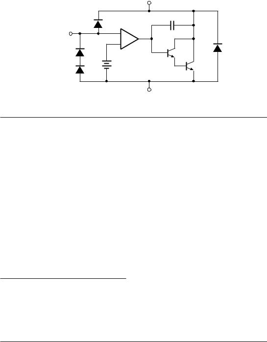
Functional Block Diagram
CATHODE (K)
REFERENCE |
+ |
(R) |
|
|
Ð |
|
2.5 V |
ANODE (A)
Absolute Maximum Ratings
Parameter |
Symbol |
Rating |
Units |
Cathode-Anode Reverse Breakdown |
VKA |
37 |
V |
Anode-Cathode Forward Current |
IAK |
1 |
A |
Operating Cathode Current |
IKA |
250 |
mA |
Reference Input Current |
IREF |
10 |
mA |
Continuous Power at 25¡C |
PD |
|
|
TO-92 |
|
775 |
mW |
8L SOIC |
|
750 |
mW |
SOT-89 |
|
1000 |
mW |
SOT-23/5L |
|
200 |
mW |
|
|
|
|
Junction Temperature |
TJ |
150 |
¡C |
Storage Temperature |
TSTG |
Ð65 to 150 |
¡C |
Lead Temperature, Soldering 10 Seconds |
TL |
300 |
¡C |
Stresses greater than those listed under ABSOLUTE MAXIMUM RATINGS may cause permanent damage to the device. This is a stress rating only and functional operation of the device at these or any other conditions above those indicated in the operational sections of this specification is not implied. Exposure to absolute maximum rating conditions for extended periods may affect reliability.
Recommended Conditions
Parameter |
Symbol |
Rating |
Unit |
Cathode Voltage |
VKA |
VREF to 20 |
V |
Cathode Current |
IK |
10 |
mA |
Typical Thermal Resistances
Package |
θJA |
θJC |
Typical Derating |
TO-92 |
160¡C/W |
80¡C/W |
6.3 mW/¡C |
|
|
|
|
SOIC |
175¡C/W |
45¡C/W |
5.7 mW/¡C |
|
|
|
|
SOT-89 |
110¡C/W |
8¡C/W |
9.1 mW/¡C |
|
|
|
|
SOT-23/5L |
575¡C/W |
150¡C/W |
1.7 mW/¡C |
|
|
|
|
ASTEC Semiconductor |
2 |

Precision Adjustable Shunt Reference |
AS431 |
Electrical Characteristics
Electrical Characteristics are guaranteed over full junction temperature range (0 to 105¡C). Ambient temperature must be derated based on power dissipation and package thermal characteristics. The conditions are: VKA = VREF and IK = 10 mA unless otherwise stated.
|
|
|
|
Test |
AS431 (0.25%) |
AS431 (0.5%) |
|
Test |
|||||
Parameter |
Symbol |
Condition |
Min. |
Typ. |
Max. |
Min. |
Typ. |
Max. |
Unit |
Circuit |
|||
|
|
|
|
|
|
|
|
|
|
|
|
|
|
Reference Voltage |
|
VREF |
TA = 25¡C |
2.496 |
2.503 |
2.509 |
2.490 |
2.503 |
2.515 |
V |
1 |
||
|
|
|
|
Over temp. |
2.475 |
|
2.530 |
2.469 |
|
2.536 |
V |
1 |
|
|
|
|
|
|
|
|
|
|
|
|
|
|
|
ÆVREF with Temp* |
|
TC |
|
|
0.07 |
0.20 |
|
0.07 |
0.20 |
mV/¡C |
1 |
||
Ratio of Change in |
|
ÆVREF |
VREF to 10 V |
Ð2.7 |
Ð1.0 |
|
Ð2.7 |
Ð1.0 |
|
|
|
||
VREF to Cathode |
|
ÆVK |
|
|
|
|
|
|
|
|
mV/V |
2 |
|
10 V to 36 V |
Ð2.0 |
Ð0.4 |
0.3 |
Ð2.0 |
Ð0.4 |
0.3 |
|||||||
Voltage |
|
|
|
|
|
||||||||
Reference Input |
|
IREF |
|
|
0.7 |
4 |
|
0.7 |
4 |
µA |
2 |
||
Current |
|
|
|
|
|
|
|
|
|
|
|
|
|
|
|
|
|
|
|
|
|
|
|
|
|
||
IREF Temp Deviation |
|
ÆIREF |
Over temp. |
|
0.4 |
1.2 |
|
0.4 |
1.2 |
µA |
2 |
||
Min IK for Regulation |
|
IK(min) |
|
|
0.4 |
1 |
|
0.4 |
1 |
mA |
1 |
||
Off State Leakage |
|
IK(off) |
VREF = 0 V, |
|
0.04 |
250 |
|
0.04 |
250 |
nA |
3 |
||
|
|
|
|
VKA = 36 V |
|
|
|
|
|
|
|
|
|
Dynamic Output |
|
ZKA |
f ² 1 kHz |
|
0.15 |
0.5 |
|
0.15 |
0.5 |
½ |
1 |
||
Impedance |
|
|
|
IK = 1 to 150 mA |
|
|
|
|
|
|
|
|
|
|
|
|
|
Test |
AS431 (1.0%) |
AS431 (2.0%) |
|
Test |
|||||
Parameter |
Symbol |
Condition |
Min. |
Typ. |
Max. |
Min. |
Typ. |
Max. |
Unit |
Circuit |
|||
|
|
|
|
|
|
|
|
|
|
|
|
|
|
Reference Voltage |
|
VREF |
TA = 25¡C |
2.470 |
2.495 |
2.520 |
2.440 |
2.490 |
2.550 |
V |
1 |
||
|
|
|
|
Over temp. |
2.449 |
|
2.541 |
2.430 |
|
2.569 |
V |
1 |
|
|
|
|
|
|
|
|
|
|
|
|
|
|
|
ÆVREF with Temp* |
|
TC |
|
|
0.07 |
0.20 |
|
0.07 |
0.20 |
mV/¡C |
1 |
||
Ratio of Change in |
|
ÆVREF |
VREF to 10 V |
Ð2.7 |
Ð1.0 |
|
Ð2.7 |
Ð1.0 |
|
|
|
||
VREF to Cathode |
|
ÆVK |
|
|
|
|
|
|
|
|
mV/V |
2 |
|
10 V to 36 V |
Ð2.0 |
Ð0.4 |
0.3 |
Ð2.0 |
Ð0.4 |
0.3 |
|||||||
Voltage |
|
|
|
|
|
||||||||
Reference Input |
|
IREF |
|
|
0.7 |
4 |
|
0.7 |
4 |
µA |
2 |
||
Current |
|
|
|
|
|
|
|
|
|
|
|
|
|
|
|
|
|
|
|
|
|
|
|
|
|
||
IREF Temp Deviation |
|
ÆIREF |
Over temp. |
|
0.4 |
1.2 |
|
0.4 |
1.2 |
µA |
2 |
||
Min IK for Regulation |
|
IK(min) |
|
|
0.4 |
1 |
|
0.4 |
1 |
mA |
1 |
||
Off State Leakage |
|
IK(off) |
VREF = 0 V, |
|
0.04 |
250 |
|
0.04 |
250 |
nA |
3 |
||
|
|
|
|
VKA = 36 V |
|
|
|
|
|
|
|
|
|
Dynamic Output |
|
ZKA |
f ² 1 kHz |
|
0.15 |
0.5 |
|
0.15 |
0.5 |
½ |
1 |
||
Impedance |
|
|
|
IK = 1 to 150 mA |
|
|
|
|
|
|
|
|
|
*Calculating Average Temperature Coefficient (TC). Refer to following page.
ASTEC Semiconductor |
3 |
 Loading...