


ASTEC AS273H5LPT, AS273H5LPB, AS273H5LPA, AS273H5LP13, AS273H1LPA Datasheet
...
SEMICONDUCTOR
AS273
Over-Temperature Detector
Features
¥Programmable to three different over-temperature thresholds
¥2.5 V temperature compensated bandgap reference trimmed to 1%
¥Open collector output goes low on over-temp condition
¥±3¡C temperature accuracy
¥Reference shunt current serves to program over-temp threshold
¥Available with 5¡C or 10¡C of temperature hysteresis
¥Available in a wide range of overtemp thresholds to fit most temperature monitoring applications
¥Now available in the SOT-223 for improved substrate temperature sensing
Description
The AS273 is a series of programmable over-temperature detectors. Each is internally composed of a precision 2.5 V shunt reference, a proportional-to-absolute temperature thermal sensor, a comparator with controlled hysteresis, and an open collector output that indicates an over-temp condition. The threshold for the over-temp signal can be set to any of three values on a given part by controlling the magnitude of the reference shunt current.
The AS273 has an excellent absolute temperature accuracy of ±3¡C for each of the three over-temp thresholds. The low power dissipation minimizes any temperature sensing errors due to self-heating. There is either 5¡C or 10¡C of temperature hysteresis to prevent bouncing when an over-temp condition is removed.
The packaging options available with the AS273 make it appealing to a wide variety of temperature-sensing applications. The TO-92 package can be mechanically clamped to a heat sink to monitor the temperature of power devices. The 8L-SOIC and SOT-223 surface mount packages allow for temperature sensing in high component density applications.
Pin Configuration Ñ Top view
SOIC (D) |
TO-92 (LP) |
SOT-223 (G) |
OUT |
1 |
8 |
N/C |
2 |
7 |
N/C |
3 |
6 |
N/C |
4 |
5 |
VREF
DO NOT USE
DO NOT USE
GROUND
|
OUT |
OUT |
|
GROUND |
GROUND |
|
|
VREF |
VREF |
|
ASTEC Semiconductor |
1 |
AS273 |
|
|
|
|
|
|
|
|
|
|
|
|
|
|
|
|
|
Over-Temperature Detector |
||||
Ordering Information |
|
|
|
|
|
|
|
|
|
|
|
|
|
|
|
|
|
|
|
|||
|
|
|
|
|
AS273 D 1 D A |
|
|
|
|
|||||||||||||
|
Circuit Type: |
|
|
|
|
|
|
|
|
|
|
|
|
|
|
|
|
|
|
|
Packaging Option: |
|
|
Over-Temperature Detector |
|
|
|
|
|
|
|
|
|
|
|
|
|
|
|
|
|
A |
= Ammo Pack |
||
|
Temperature Option: |
|
|
|
|
|
|
|
|
|
|
|
|
|
|
|
|
|
|
B |
= Bulk |
|
|
|
|
|
|
|
|
|
|
|
|
|
|
|
|
|
|
|
|
T |
= Tube |
||
|
|
|
|
|
|
|
|
|
|
|
|
|
|
|
|
|||||||
|
(Refer to Table A) |
|
|
|
|
|
|
|
|
|
|
|
|
|
|
|
|
|
13 = Tape and Reel (13" Reel Dia) |
|||
|
Table A – Temperature Options |
|
|
|
|
|
|
|
|
|
|
|
|
|
|
|
|
|
Package Style: |
|||
|
|
|
|
|
|
|
|
|
|
|
|
|
|
|
|
|
|
|||||
|
|
|
|
|
|
|
|
|
|
|
|
|
|
|
|
|
|
D |
= SOIC |
|||
|
Code |
TOT1 |
TOT2 |
|
TOT3 |
|
|
|
|
|
|
|
|
|
|
|
|
|||||
|
|
|
|
|
|
|
|
|
G |
= SOT-223 |
||||||||||||
|
D |
40 |
|
45 |
50 |
|
|
|
|
|
|
|
|
|
|
|
|
|
|
|||
|
|
|
|
|
|
|
|
|
|
|
|
|
|
|
|
LP = TO-92 |
||||||
|
F |
75 |
|
80 |
85 |
|
|
|
|
|
|
|
|
|
|
|
|
|
|
|
|
|
|
G |
90 |
|
95 |
100 |
|
|
|
|
|
|
|
|
|
|
|
|
|
Hysteresis Option: |
|||
|
|
|
|
|
|
|
|
|
|
|
|
|
||||||||||
|
|
|
|
|
|
|
|
|
|
|
|
|
|
|
|
|
|
1 = 10°C |
||||
|
H |
105 |
110 |
115 |
|
|
|
|
|
|
|
|
|
|
|
|
|
|||||
|
|
|
|
|
|
|
|
|
|
|
|
|
|
|
|
|
|
|
|
|
5 = 5°C |
|
|
|
|
|
|
|
|
|
|
|
|
|
|
|
|
|
|
|
|
|
|
||
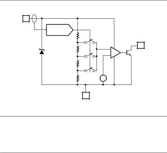
Functional Block Diagram
VREF
1 |
CURRENT
PROGRAMMING
OUT
3
+
2.5 V
Ð
4 mV/K |
+ |
|
Ð |
||
|
2 |
GND
Pin Function Description
Pin Number |
Function |
Description |
1 |
VREF |
2.5 V shunt reference; current into VREF pin also programs |
|
|
over-temperature trip point to one of three TOT values |
2 |
GND |
Circuit ground and silicon substrate |
|
|
|
3 |
OUT |
Open collector output. Output low when die temperature exceeds |
|
|
programmed trip point |
|
|
|
ASTEC Semiconductor |
2 |

Over-Temperature Detector |
|
|
AS273 |
Absolute Maximum Ratings |
|
|
|
|
|
|
|
Parameter |
Symbol |
Rating |
Unit |
|
|
|
|
Reference Current |
VREF |
±10 |
mA |
Output Current |
IOUT |
±10 |
mA |
Output Voltage |
VOUT |
18 |
V |
Continuous Power Dissipation at 25¡C |
|
|
|
TO-92 |
PD |
775 |
mW |
8-SOIC |
PD |
750 |
mW |
SOT-223 |
PD |
1000 |
mW |
Junction Temperature |
TJ |
150 |
¡C |
Storage Temperature |
TSTG |
Ð65 to 150 |
¡C |
Lead Temp, Soldering 10 Seconds |
TL |
300 |
¡C |
Stresses greater than those listed under ABSOLUTE MAXIMUM RATINGS may cause permanent damage to the device. This is a stress rating only and functional operation of the device at these or any other conditions above those indicated in the operational sections of this specification is not implied. Exposure to absolute maximum rating conditions for extended periods may affect reliability.
Typical Thermal Resistances
Package |
θJA |
θJC |
Typical Derating |
SOT-223 |
115¡C/W |
8¡C/W |
8.7 mW/¡C |
|
|
|
|
TO-92 |
160¡C/W |
80¡C/W |
6.3 mW/¡C |
|
|
|
|
8L SOIC |
175¡C/W |
45¡C/W |
5.7 mW/¡C |
|
|
|
|
ASTEC Semiconductor |
3 |

AS273 |
Over-Temperature Detector |
Electrical Characteristics
Electrical Characteristics are guaranteed over the full junction temperature range (0 to 125¡C). Ambient temperature must be derated based upon power dissipation and package thermal characteristics.
Parameter |
Symbol |
Test Condition |
Min. |
Typ. |
Max. |
Unit |
|
|
|
|
|
|
|
Reference |
|
|
|
|
|
|
|
|
|
|
|
|
|
Reference Voltage |
VREF |
IREF = 2 mA, TJ = 25¡C |
2.500 |
2.525 |
2.550 |
V |
Load Regulation |
VId |
0.65 mA ≤ IREF ≤ 5.5 mA |
|
5 |
10 |
mV |
Average Temperature Coefficient |
VREG/ T |
0.65 mA ≤ IREF ≤ 5.5 mA |
|
75 |
|
ppm/¡C |
Output |
|
|
|
|
|
|
|
|
|
|
|
|
|
Saturation Voltage |
VOL |
IOUT = 4 mA; TJ > TOT |
|
200 |
400 |
mV |
Breakdown Voltage |
BV |
IOUT = 100 µA; TJ < TOT |
18 |
30 |
|
V |
Leakage Current |
IOH |
VOUT = 18 V; TJ < TOT |
|
1 |
1000 |
nA |
Over-Temp Sensing |
|
|
|
|
|
|
|
|
|
|
|
|
|
Temperature Accuracy |
TOT(1) |
0.7 mA ≤ IREF ≤ 1.3 mA |
Ð3 |
|
+3 |
¡C |
|
TOT(2) |
1.55 mA ≤ IREF ≤ 2.6 mA |
Ð3 |
|
+3 |
¡C |
|
TOT(3) |
3.0 mA ≤ IREF ≤ 5.0 mA |
Ð3 |
|
+3 |
¡C |
Hysteresis |
HOT |
Percentage Error in Nominal Hysteresis |
Ð30 |
|
+30 |
% |
Test Circuit
+5V
RLOAD
2 kΩ
|
|
VREF |
|
|
|
|
|
|
OUT |
|
|
|
|
||||||||
|
|
|
AS273 |
|
||||||
IREF |
|
|
GND |
|
||||||
|
|
|
||||||||
|
|
|
|
|
|
|
|
|
|
|
|
|
|
|
|
|
|
|
|
|
|
|
|
|
|
|
|
|
|
|
|
|
|
|
|
|
|
|
|
|
|
|
|
Figure 1. Test Circuit for Output Hysteresis Curve
ASTEC Semiconductor |
4 |
 Loading...