Arcam Alpha 10-P Service manual


ALPHA 10/10P SERVICE MANUALALPHA 10/10P SERVICE MANUAL
ALPHA 10/10P SERVICE MANUAL
CIRCUIT DESCRIPTION
The mother PCB is common for both the A10 and A10P with the exception of the input mode switch and pre-amp
output mute relay which are only fitted to the A10 and the power/standby LED and links to parallel the input
connections to what would otherwise be the pre-amp output for use with a mono link. The amplifier is based on the
D290/Alpha 9 design but with lower gain, a higher current and higher voltage driver stage and a high power output
stage. The current servo has been improved over the Alpha 9 to be output device independent. A micro supervises
the amplifier state, switch state and remote control functions. Provision is made for an additional 3rd channel PCB to
be added with power supply and protection circuitry access.
Input stage
The input connections are taken either from the pre-amp connector, LK12X, or the external power amp input on the
A10 depending on the position of SW1. On the A10P, the input is taken from the external power amp input only with
provision for a mono shorting link by having two parallel input connectors. On the A10, there is a mute relay on the
pre-amp outputs which are always connected to the pre-amp connector, LK12X.
The signal is passed through a low pass filter with a -3dB point of 550KHz at normal gain and 740KHz at low gain.
The gain is selected by SW2. C72 and C74 are d.c. blocking capacitors with a -3dB point of 0.7Hz. A d.c. error
correction current is injected into the base of Q19 and 26 from the voltage servo Z3 and 4, to null any voltage offset at
the amplifier output.
The input and voltage amplifier stages both run off regulated 15 Volt suppies. The input stage is an NPN differential
input, Q18, 19, 25 and 26, with an adjustable current source, Q21 and 28 which sets the quiescent current through all
the stages but specifically the output stage. C37, R58, C49 and R66 keep the input stage and voltage amplifier stable.
Q52, 53, 54 and 55 form a current mirror to ensure that the differential input is balanced during normal operation.
Voltage Amplifier
The voltage amplifier consists of another differential pair, Q48, 49, 50 and 51. Q48 and 50 are the positive pulling side
of the voltage amplifier output and Q49 and 51 pull negative via a current mirror Q8, 9, 10 and 11. The network C12,
36, R74 and 77 give the current mirror gain to compensate for the fact that Q49 and Q51 is only driven from the lowimpedance side of the input stage current mirror. The network ensures a fast, symmetrical slew rate of the voltage
amplifier stage.
Network C69, 70, R172, 174 ensure the overall stability of the amplifier by reducing the open loop gain at high
frequencies.
Second Voltage Amplifier and Driver Stage
Q33, 36, 41 and 44 are the next voltage amplifier stage with feedback applied from the output coupled to their
emitters. This stage runs on the full supply rail voltages and splits the level shifts the signal via Q2, 3, 5 and 6 to drive
the gates of the output MOSFETs, Q13, 14, 15 and 16. Q2 and 3 simply buffer the inverted signal at the collector of
Q36 to drive the low side MOSFETs, Q13 and 15. Q5 and 6 invert the inverted signal at the collector of Q41 and Q44
to drive the high side MOSFETs, Q14 and 16. To ensure that the high side drive is able to swing far enough to ensure
the high side MOSFETs can be driven to saturation, a bootstrap, C5, D41 R57, C78 and D22 boosts the driver stage
power supply during positive excursions of the amplifier output. This is inactive at low output voltage swings as any
distortion induced by the network would be more audible at such levels.
Output Stage
Both the high and low side output devices feature over-current protection, Q17, 23, 24, 30 which clamps the gate of
the MOSFET it protects. A high current is permitted through the MOSFET for a few milliseconds after which time the
current is throttled down to about 10A peak. A second current sensing network, Q32 and Q35 activates the
over-current protection cut-out if the low side is current limiting for too long, a few hundred milliseconds. The current
sensing resistors do not reduce the transconductance of the MOSFETs because the driver stage is referenced to the
MOSFET source. This means that the current through the driver stage is also sensed but this is insignificant as fas as
over-current protection sensing is concerned.
Auto-bias
1

ALPHA 10/10P SERVICE MANUALALPHA 10/10P SERVICE MANUAL
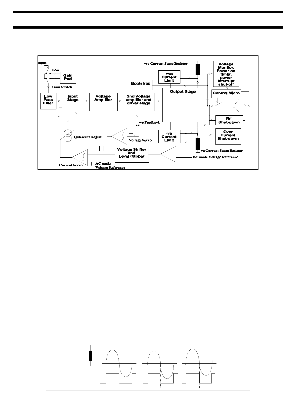
Figure 1Block Diagram of Power Amplifier
The bias is regulated in two modes, one where these is no signal and one when signal is being split between the high
and low side MOSFETs when driving a alternating signal into a load.
Under static conditions, Z8 simply compares the sensed current, which includes the driver stage current, with a d.c.
mode reference of 13mV. The sense resistor is 0.11 so this corresponds to a current of about 120mA, some of which
is driver current. The current through the MOSFETs is about 80mA at this point. The comparator output is level shifted
to drive the integrating current servos Z3 and 4. This adjusts the amplifier current so that, on average, the bias level is
held at the reference point.
Under dynamic conditions, the low side drive will definitely be conducting more current than the reference (80mA) for
half the signal cycle and will be switched off for the other half. The result is a rectangle wave output from the
comparator, Z4.
When the output stage is biassed correctly (class AB operation) the comparator output toggles when the current
through the sense resistor for the -ve MOSFET is equal to the d.c. mode static reference level and at the half way
point of the signal. The result is a perfect square wave output from the comparator. Under these conditions, the +ve
MOSFET is also conducting the same amount of current at this point. If the bias level is lower than the reference, say,
at zero (class B operation) then the -ve MOSFET will spend slightly less than half the time conducting at or above the
reference level resulting in a rectangle wave output from the comparator at a duty cycle slightly less than 50%. If the
bias level is higher than the reference then the -ve MOSFET will spend slightly more than half the time conducting at
or above the reference level resulting in a rectangle wave output at a duty cycle slightly more than 50%. The change
in duty cycle away from 50% causes the integrator, Z3 and Z4 to adjust the bias level via the bias adjusting
transistors, Q22 and 29.
The integrator has a reference, the a.c. mode dynamic reference, for a bias point slightly higher than for a 50% duty
cycle. This eliminates the possibility of the bias being slowly throttled due to component tolerance mismatch resulting
in a reference which would pull the servo down. A high dynamic bias reference level simply stabilises the bias slightly
higher than the static reference but a low dynamic reference causes the bias to drift down to complete throttle.
This system works if the signal is a.c., symmetrical and is not a rectangle wave. Certainly, only a.c. signals are passed
Sense Resistor
Comparitor Output
-ve MOSFET
Measured Current (blue)
Other MOSFET
50%
Bias correct Under Biassed Over Biassed
49% 52%
Figure 2 Auto-bias under dynamic conditions
2

ALPHA 10/10P SERVICE MANUALALPHA 10/10P SERVICE MANUAL
through the amplifier due to C72 and 74 d.c. blocking capacitors and on average the signal will be symmetrical. Any
short-term asymmetry will be ironed out by the long time constant of the integrator.
Main Power Supply
The main power supply is regulated in two stages. First it is pre-regulated by Q1 and 4 to about 11V less than the
main supply rails. This supply is made available to an option board. The maximum load on these supplies is 150mA
for less than 2W dissipation in Q1 and 4. These supplies are then regulated to +/-15V by Z1 and 2. These supplies are
used by the input stages of the power amplifiers including any 3rd channel board, the pre-amplifier board and an
optional phono amplifier board. The positive voltage regulator, Z1, has a larger heatsink than Z2 because the phono
board consumes much more current from the positive rail than from the negative rail.
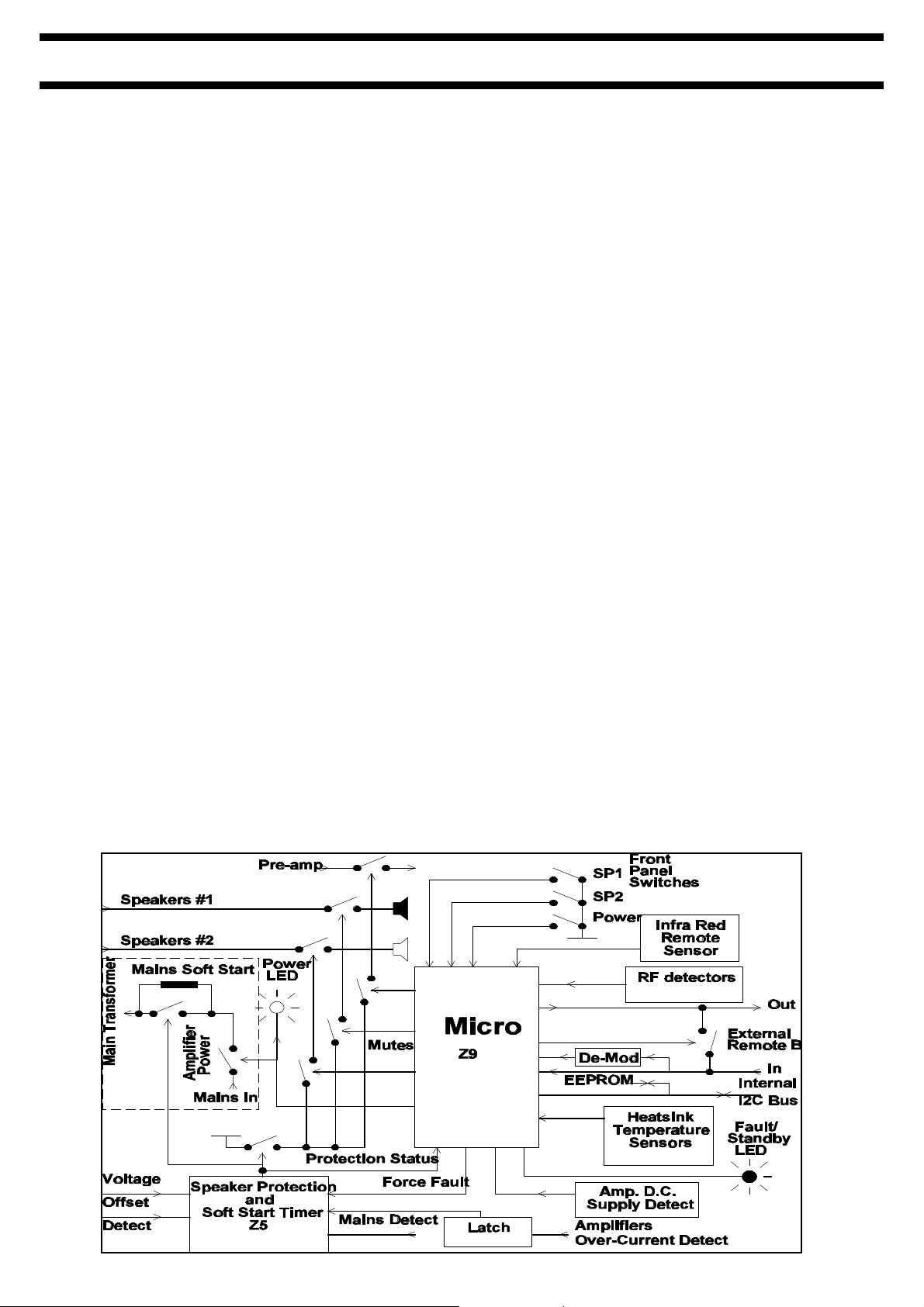
Control Micro
The control micro performs the following functions...
‚ Switches the amplifier on or off,
‚ Mutes the speakers #1 or #2 or the pre-amp output,
‚ Monitors the heatsink temperature,
‚ Monitors RF content of speaker outputs,
‚ Handles the remote bus and infra red remote input,
‚ Reports fault conditions to the main display and LED,
‚ Reads the speaker and power switch positions.
The control micro runs of the constant power supply from standby transformer, TX2. This enables the amplifier to be
switched on or off remotely from the remote bus or, in the case of the integrated amplifier, from an infra red remote
control. This power supply is intended to supply all the digital circuitry in the amplifier including any option boards.
This is supplied at 8V to the other boards where it will be locally regulated to 5V as required.
The micro communicates with the display board via a multi-master I2C bus. This bus is used to report amplifier and
power status to the display micro and remote control commands received. It is also possible for the display micro to
control functions on the power amplifier board. The option board also uses this bus to receive any remote control
commands and communicate with the display micro.
The external remote bus handles raw information from infra red sensors with no demodulating. The remote bus input
can be echoed to the output through a buffer circuit. The incoming signal is demodulated by Z13. Raw signal is also
sent to the micro interrupt line, pin 12, for assessing the noise on the remote bus. In addition, any d.c. signal on the
remote bus is sensed on pin 2 of the micro in when it is not being used as an output to mute the hardware remote
echo buffer. The micro must modulate any output it sends to this bus with a carrier (37KHz). The output will drive one
or two series infra red LEDs directly.
The list below shows how various fault conditions can be deduced simply from the Power LED behaviour.
Figure 3 Micro Block Diagram
3

ALPHA 10/10P SERVICE MANUALALPHA 10/10P SERVICE MANUAL
• On power up, the protection should be engaged. This is checked after 3 seconds on pin 9 of Z9. If it isn't
happening, the unit shuts down with flashing red.
• If the protection does not clear after about 16 seconds on power-up the unit shuts down to flashing red. This
is usually caused by a voltage offset.
• Any main amp power loss detected on pin 26 after power-up causes a shut down to flashing red.
• Any RF detected on pin 3 results on immediate shut down to flashing red.
• Any protection fault detected after power up on pin 9 results in a flashing amber LED for about 16 seconds
max. If it has not cleared by then the unit is shut down to flashing red. Protection faults are caused by voltage
offset or over-current. Over-current should latch resulting in a shut down after 16 seconds. Voltage offsets
should clear themselves if brief.
• A temperature fault on pin 25 results in the power LED flashing slow amber and can last indefinitely until it
clears. When it clears the flashing will speed up until the protection times back in.
ALPHA 10P POWER AMP MAIN BOARD PARTS LIST
Ref No. Description Part No
C1 ELST 100U 100V 2N710B
C2 ELST 100U 100V 2N710B
C3 MLC 100N 50V X7R 10% SM 2C410
C4 ELST 100U 100V 2N710B
C5 ELST 100U 100V 2N710B
C6 ELST 22U 63V 2N622
C7 ELST 10U 50V 2N610
C8 ELST 22U 63V 2N622
C9 ELST 10U 50V 2N610
C10 ELST 10U 50V 2N610
C11 ELST 1U0 50V 2N510
C12 PPRO 4N7 63V 5% RA 2D247N
C13 SUPPR CAP 4N7 250V 2K247
C14 PPRO 150P 5% 63V RA 2D115
C15 ELST 10U 50V 2N610
C16 ELST 10U 50V 2N610
C17 ELST 10U 50V 2N610
C18 ELST TNC 10m 63V RA 40mm 2N910A
C19 ELST TNC 10m 63V RA 40mm 2N910A
C20 PPRO 4N7 63V 5% RA 2D247N
C21 PPRO 4N7 63V 5% RA 2D247N
C22 ELST 100U 25V 2N710
C23 ELST 100U 25V 2N710
C24 ELST 100U 25V 2N710
C25 ELST 100U 25V 2N710
C26 ELST 100U 25V 2N710
C27 ELST 100U 25V 2N710
C28 MLC 470P 100V NPO 5% SM 2C147
C29 MLC 470P 100V NPO 5% SM 2C147
C30 MLC 470P 100V NPO 5% SM 2C147
C31 MLC 100N 50V X7R 10% SM 2C410
C32 ELST 22U 63V 2N622
C33 ELST 22U 63V 2N622
C34 MLC 100N 50V X7R 10% SM 2C410
C35 PPRO 150P 5% 63V RA 2D115
C36 PPRO 4N7 63V 5% RA 2D247N
C37 PPRO 1N0 5% 63V RA 2D210
C38 PPRO 680P 63V 5% RA 2D168
C39 PPRO 680P 63V 5% RA 2D168
C40 MLC 10N 50V X7R 10% SM 2C310
C41 MLC 10N 50V X7R 10% SM 2C310
C42 MLC 10N 50V X7R 10% SM 2C310
C43 MLC 10N 50V X7R 10% SM 2C310
C44 SUPPR CAP 4N7 250V 2K247
C45 ELST 10U 50V 2N610
C46 SUPPR CAP 4N7 250V 2K247
C47 SUPPR CAP 4N7 250V 2K247
C48 ELST 3M3 25V 2N833
C49 PPRO 1N0 5% 63V RA 2D210
C50 ELST 1U0 50V 2N510
C51 ELST 220U 16V 2N722
C52 ELST 220U 16V 2N722
C53 ELST 220U 16V 2N722
C54 ELST 220U 16V 2N722
C55 PCRB 100N 100V 10% RA 5mm 2H410
C56 PCRB 100N 100V 10% RA 5mm 2H410
C57 PCRB 100N 100V 10% RA 5mm 2H410
C58 PCRB 100N 100V 10% RA 5mm 2H410
C59 PCRB 100N 100V 10% RA 5mm 2H410
C60 PCRB 100N 100V 10% RA 5mm 2H410
C61 PPRO 100P 63V 5% RA 2D110N
4

ALPHA 10/10P SERVICE MANUALALPHA 10/10P SERVICE MANUAL
C62 PPRO 100P 63V 5% RA 2D110N
C63 PPRO 150P 5% 63V RA 2D115
C64 PPRO 330P 5% 63V RA 2D133
C65 PPRO 150P 5% 63V RA 2D115
C66 PPRO 330P 5% 63V RA 2D133
C67 PEST 15N 63V 5% 2K315
C68 PEST 15N 63V 5% 2K315
C69 PSTY 56P 160V ENCAP 1PF% 2F056
C70 PSTY 56P 160V ENCAP 1PF% 2F056
C71 ELST NON POLAR 10UF 35V 2U610
C72 ELST NON POLAR 10UF 35V 2U610
C73 ELST NON POLAR 10UF 35V 2U610
C74 ELST NON POLAR 10UF 35V 2U610
C75 PEST 47N 63V 10% 2K347
C76 PEST 47N 63V 10% 2K347
C77 PEST 47N 63V 10% 2K347
C78 PEST 47N 63V 10% 2K347
C79 ELST NON POLAR 10UF 35V 2U610
C80 ELST NON POLAR 10UF 35V 2U610
C81 MLC 22P 100V NPO 5% SM 2C022
C82 MLC 22P 100V NPO 5% SM 2C022
C83 ELST 100U 25V 2N710
C84 MLC 100N 50V X7R 10% SM 2C410
C85 MLC 100N 50V X7R 10% SM 2C410
C86 MLC 100N 50V X7R 10% SM 2C410
C87 MLC 100N 50V X7R 10% SM 2C410
C88 MLC 100N 50V X7R 10% SM 2C410
C89 MLC 100N 50V X7R 10% SM 2C410
C90 ELST 10U 50V 2N610
C91 PPRO 680P 63V 5% RA 2D168
C92 MLC 10N 50V X7R 10% SM 2C310
C93 MLC 1N0 50V X7R 10% SM 2C210
C94 MLC 10N 50V X7R 10% SM 2C310
C95 ELST 10U 50V 2N610
C96 ELST 10U 50V 2N610
C97 MLC 100N 50V X7R 10% SM 2C410
C98 MLC 10N 50V X7R 10% SM 2C310
C99 CERD 10PF 63V 10% 2A010
C100 CERD 10PF 63V 10% 2A010
D1 ZENER 15V 400MW 3C11504
D2 ZENER 15V 400MW 3C11504
D3 ZENER 10V 400MW 3C11004
D4 ZENER 10V 400MW 3C11004
D5 ZENER 10V 400MW 3C11004
D6 ZENER 10V 400MW 3C11004
D7 ZENER 10V 400MW 3C11004
D8 ZENER 10V 400MW 3C11004
D9 ZENER 10V 400MW 3C11004
D10 RECTIFIER 6A40 6A 400V 3B6A40
D11 RECTIFIER 6A40 6A 400V 3B6A40
D12 RECTIFIER 6A40 6A 400V 3B6A40
D13 RECTIFIER 6A40 6A 400V 3B6A40
D14 RECTIFIER 1N4003F 1A 200V 3B4003
D15 RECTIFIER 1N4003F 1A 200V 3B4003
D16 SSDIODE 1N4148 75V 3A4148
D17 SSDIODE 1N4148 75V 3A4148
D18 RECTIFIER 1N4003F 1A 200V 3B4003
D19 RECTIFIER 1N4003F 1A 200V 3B4003
D20 SSDIODE 1N4148 75V 3A4148
D21 RECTIFIER 1N4003F 1A 200V 3B4003
D22 RECTIFIER 1N4003F 1A 200V 3B4003
D23 RECTIFIER 1N4003F 1A 200V 3B4003
D24 RECTIFIER 1N4003F 1A 200V 3B4003
D25 RECTIFIER 1N4003F 1A 200V 3B4003
D26 SSDIODE 1N4148 75V 3A4148
D27 RECTIFIER 1N4003F 1A 200V 3B4003
D28 SSDIODE 1N4148 75V 3A4148
D29 ZENER 4V7 400MW 3C04704
D30 SSDIODE 1N4148 75V 3A4148
D31 SSDIODE 1N4148 75V 3A4148
D32 SSDIODE 1N4148 75V 3A4148
D33 SSDIODE 1N4148 75V 3A4148
D34 SSDIODE 1N4148 75V 3A4148
D35 SSDIODE 1N4148 75V 3A4148
D36 SSDIODE 1N4148 75V 3A4148
D37 SSDIODE 1N4148 75V 3A4148
D38 SSDIODE 1N4148 75V 3A4148
D39 ZENER 12V 3W SM 3C03C12
D40 SSDIODE 1N4148 75V 3A4148
D41 ZENER 12V 3W SM 3C03C12
D42 SSDIODE 1N4148 75V 3A4148
D43 ZENER 5V6 400MW 3C05604
D44 ZENER 24V 3W SM 3C03C24
D45 RECTIFIER 1N4003F 1A 200V 3B4003
D46 SSDIODE 1N4148 75V 3A4148
D47 SSDIODE 1N4148 75V 3A4148
5
 Loading...