

Page 1

MODEL
373XXA
VECTOR NETWORK ANALYZER
MAINTENANCE MANUAL
490 JARVIS DRIVE l MORGAN HILL, CA 95037-2809
P/N: 10410-00185
REVISION: D
PRINTED: MARCH 2000
COPYRIGHT 1996 ANRITSU CO.
Page 2

WARRANTY
The ANRITSU product(s) listed on the title page is (are) warranted against defects in materials and
workmanship for one year from the date of shipment.
ANRITSU’sobligation covers repairing or replacing products which prove to be defective during the
warranty period. Buyers shall prepay transportation charges for equipment returned to ANRITSU
for warranty repairs. Obligation is limited to the original purchaser.ANRITSU is not liable for con
sequential damages.
LIMITATION OF WARRANTY
The foregoing warranty does not apply to ANRITSU connectors that have failed due tonormal wear.
Also, the warranty does not apply to defects resulting from improper or inadequate maintenance by
the Buyer, unauthorized modification or misuse, or operation outside of the environmental specifications of the product. No other warranty is expressed or implied, and the remedies provided herein
are the Buyer’s sole and exclusive remedies.
TRADEMARK ACKNOWLEDGEMENTS
V Connector and K Connector are registered trademarks of ANRITSU Company.
ANACAT is a registered trademark of EEsof, Inc.
Ink Jet and Think Jet are registered trademarks of Hewlett-Packard Co.
MS-DOS is a registered trademark of Microsoft Corporation.
NOTICE
-
ANRITSU Company has prepared this manual for use by ANRITSU Company personnel and cus
tomers as a guide for the proper installation, operation and maintenance of ANRITSU Company
equipment and computer programs. The drawings, specifications, and information contained herein
are the property of ANRITSU Company, and any unauthorized use or disclosure of these drawings,
specifications, and information is prohibited; they shall not be reproduced, copied, or used in whole
or in part as the basis for manufacture or sale of the equipment or software programs without the
prior written consent of ANRITSU Company.
-
Page 3

Table of Contents, Narrative
Chapter 1 — General Service Information
This chapter provides a general description of Series373XXA Vector Network Analyzer systems, sys
tem serial numbers, and frequency ranges. It explains the level of maintenance covered in this man
ual and the service strategy used throughout this manual. It also contains static-sensitive component
handling precautions and a list of recommended test equipment.
Chapter 2 — Replaceable Parts
This chapter lists all replaceable subassemblies and components for all373XXA models. It explains
the ANRITSUexchange assembly program and provides parts ordering information.
Chapter 3 — Operational Tests
This chapter contains procedures that provide a means of fully testing the373XXA VNA system for
proper operation and signal stability. These tests are intended to be used as a periodic check of the
operational functionality of the373XXA.
Chapter 4 — Performance Verification Procedures
This chapter provides detailed procedures for verifying that the performance of the373XXA meets
minimum performance standards.
Chapter 5 — Troubleshooting
This chapter provides information for troubleshooting Series373XXA Vector Network Analyzer systems. The troubleshooting procedures contained in this chapter support fault isolation down to a replaceable subassembly.
-
-
Chapter 6 — Adjustments
This chapter provides adjustment procedures for all models of Series373XXA Vector Network Ana
lyzer systems. These procedures are used after replacement or repair of one or more critical subas
semblies, or as indicated by the Performance Verification Procedures contained in Chapter 4.
Chapter 7 — System Description
This chapter provides descriptions of the functional operation of the major assemblies contained in
Series373XXA Vector Network Analyzer systems. The operation of all major circuit blocks is de
scribed so that the reader may better understand the function of each assembly as part of the overall
operation.
Chapter 8— Removal and Replacement Procedures
This chapter describes how to gain access to all of the major assemblies and major parts for ¬trouble
shooting and/or replacement.
Appendix A — Diagnostic Menus
This appendix contains descriptions and usage information for the Diagnostic Menus that are avail
able via the front panel Option Menu key.
Appendix B — Error Codes/Messages
This appendix contains a listing of the Error Codes/Messages. Also included is a description of the in
formation fields that are part of the error messages.
-
-
-
-
-
-
373XXA MM i
Page 4

Appendix C — Connector Maintenance Check Procedures
This appendix contains procedures and information needed to perform maintenance checks (includ
ing pin-depth measurements) for the connectors on all ANRITSU supplied Calibration/Verification
Kit components, Through-cables, and other associated RF/microwave components.
Appendix D — Performance Specifications
Appendix E — Verification Software Users Guide
This appendix contains the Model 360X/372XXB VNA Performance Verification Software Users
Guide, P/N: 10410-00208. This Software Users Guide explains in detail the procedures to be used for
the installation and operation of the 373XXA VNA Verification Software on your computer/controller.
Index
-
ii 373XXA MM
Page 5

Table of Contents, Detailed
Chapter 1 General Information
1-1 SCOPE OF MANUAL ·······················1-3
1-2 INTRODUCTION ·························1-3
1-3 IDENTIFICATION NUMBER ··················1-3
1-4 ONLINE MANUAL ························1-3
1-5 SYSTEM DESCRIPTION ·····················1-4
1-6 RELATED MANUALS·······················1-4
1-7 STANDARD OPTIONS ······················1-4
1-8 SERVICE STRATEGY·······················1-5
Functional Assembly Level Troubleshooting ···········1-5
Internal Hardware Adjustments and Calibrations········1-5
Internal Service Log ························1-5
System Test/Certification ·····················1-6
Preventive Service ·························1-6
Servicing Specially Modified Instruments ············1-6
1-9 SERVICE SUPPORT ·······················1-6
Technical Support ·························1-7
Field Service Kits ·························1-7
Service Software ··························1-7
Verification Kits ··························1-8
Test Fixtures/ Aids·························1-8
Failed Assembly Exchange Program ···············1-8
1-10 PERFORMANCE SPECIFICATIONS ··············1-9
1-11 SERVICE CENTERS ·······················1-9
1-12 STATIC SENSITIVE COMPONENT HANDLING
PROCEDURES ··························1-9
1-13 RECOMMENDED TEST EQUIPMENT ·············1-9
373XXA MM iii
Page 6

Chapter 2 Replaceable Parts
2-1 INTRODUCTION ·························2-3
2-2 EXCHANGE ASSEMBLY PROGRAM ··············2-3
2-3 REPLACEABLE SUBASSEMBLIES AND PARTS ·······2-3
2-4 PARTS ORDERING INFORMATION ··············2-4
Chapter 3 Operational Tests
3-1 INTRODUCTION ·························3-3
3-2 CHECKING THE SERVICE LOG ················3-4
3-3 SELF TEST ····························3-5
3-4 PERIPHERALS AND INTERFACES ··············3-6
LCDTest······························3-6
Front Panel Test ··························3-7
External Keyboard Interface Test·················3-7
Printer Interface Test ·······················3-7
GPIB Interface Test ························3-9
3-5 SIGNAL PATH ··························3-10
Chapter 4 Performance Verification
4-1 INTRODUCTION ·························4-3
4-2 CALIBRATION AND MEASUREMENT CONDITIONS ····4-3
Standard Conditions························4-3
Special Precautions: ························4-4
4-3 MEASUREMENT ACCURACY··················4-4
Verification Software ·······················4-4
Verification Result Determination ················4-5
4-4 VERIFICATION PROCEDURE ·················4-5
4-5 KEY SYSTEM PARAMETERS ·················4-6
Measurement Environment Considerations ···········4-6
Measurement Technique ·····················4-7
iv 373XXA MM
Page 7

Chapter 5 Troubleshooting
5-1 INTRODUCTION ·························5-3
5-2 ASSOCIATED INFORMATION IN THIS MANUAL ······5-3
5-3 RECOMMENDED TEST EQUIPMENT ·············5-4
5-4 SYSTEM DOES NOT POWER-UP ················5-4
Line Source and Interface Checks ················5-4
Power Supply Voltages Check ···················5-4
Power Supply Module Check ···················5-6
5-5 SYSTEM DOES NOT BOOT-UP ·················5-7
Boot-up Process Sequence·····················5-7
Troubleshooting Boot-up Problems ················5-8
Hard Disk Problem 1 ·······················5-8
Hard Disk Problem 2 ·······················5-9
Floppy Disk Problems ·······················5-9
Screen Display Problems·····················5-10
5-6 SYSTEM HAS ERROR CODE ·················5-10
Phase Lock Error Codes (6000 Series)··············5-11
Service Log Snap Shot Data ···················5-12
5-7 SOURCE/TEST SET/RECEIVER ················5-17
Signal Source Phase Lock Loop Assemblies···········5-17
Signal Source/Test Set Module Error Codes···········5-18
Isolation Procedures ·······················5-19
5-8 PERIPHERALS/ INTERFACE ·················5-21
CRT Display Test Failures: ···················5-21
Front Panel Test Failures: ····················5-22
External Keyboard Interface Test Failures:···········5-22
Printer Interface Test Failures: ·················5-22
GPIB Interface Test Failures: ··················5-22
5-9 MEASUREMENT IN QUESTION ···············5-22
Measurement Conditions Check List ··············5-23
Chapter 6 Adjustments
6-1 INTRODUCTION ·························6-3
6-2 LO1 CALIBRATION························6-3
Calibration Procedure ·······················6-3
Post Calibration Actions······················6-3
373XXA MM v
Page 8

6-3 LO 2 CALIBRATION ·······················6-4
Calibration Procedure ·······················6-4
Post Calibration Actions······················6-5
6-4 FREQUENCY CALIBRATION ··················6-5
Calibration Procedure ·······················6-6
Post Calibration Actions······················6-7
6-5 RF POWER/ALC CALIBRATION·················6-8
Calibration Procedure ·······················6-9
Post Calibration Actions ·····················6-10
6-6 SOURCE LOCK THRESHOLD ·················6-11
Calibration Procedure ······················6-12
Post Calibration Actions ·····················6-12
6-7 A8 ADJUSTMENT (37397A) ··················6-13
Calibration Procedure ······················6-13
Post Calibration Actions ·····················6-13
6-8 A21A2 ADJUSTMENT (37397A) ················6-14
Calibration Procedure ······················6-14
Post Calibration Actions ·····················6-15
Chapter 7 System Description
7-1 INTRODUCTION ·························7-3
7-2 SYSTEM OVERVIEW ·······················7-3
7-3 ANALOG SUBSYSTEM ASSEMBLIES ·············7-7
Signal Source Module ·······················7-7
Test Set Module ··························7-8
A7PCB, 10 MHz Timebase ···················7-9
Receiver Module ·························7-10
A8, Source Lock/ Signal Separation and Control PCB ·····7-11
IF Section ·····························7-11
A7PCB,LO3··························7-12
A5 A/D Converter PCB······················7-12
7-4 DIGITALSUBSYSTEM ASSEMBLIES·············7-13
A9 Main Processor PCB Assembly················7-13
A13 I/O Interface #1 PCB Assembly···············7-15
A14 I/O Interface #2 PCB Assembly···············7-15
A15 Graphics Processor PCB Assembly ·············7-16
A16 Hard Disk PCB Assembly··················7-16
Floppy Disk Drive Assembly···················7-16
A24 VME Bus Terminator PCB ·················7-16
vi 373XXA MM
Page 9

7-5 MAIN CHASSIS ASSEMBLIES·················7-16
A17 System Motherboard Assembly···············7-16
Front Panel Assembly ······················7-16
Rear Panel Assembly·······················7-17
A18 Rear Panel Interface PCB··················7-17
Power Supply Module ······················7-18
Internal VGA Monitor ······················7-19
Chapter 8 Remove and Replace Procedures
8-1 INTRODUCTION ·························8-3
8-2 EQUIPMENT REQUIRED ····················8-3
8-3 COVERS ······························8-4
8-4 A1–A9 AND A13–A16 PCBS ···················8-6
A1 – A9 PCBs ···························8-6
A13 – A16 PCB’s ··························8-6
8-5 A9 PCB BBRAM CHIP······················8-6
8-6 A9 PCB SRAM BATTERY····················8-10
8-7 A24 VME BUS TERMINATOR PCB ··············8-12
8-8 FRONT PANEL ASSEMBLY ··················8-12
8-9 VGA DISPLAY MONITOR ····················8-14
8-10 LIQUID CRYSTAL DISPLAY (LCD) ··············8-16
8-11 FLOPPY DISK DRIVE······················8-17
8-12 REAR PANEL ASSEMBLY ···················8-19
8-13 FAN ASSEMBLY ·························8-21
8-14 POWER SUPPLY MODULE···················8-21
8-15 A18 REAR PANEL PCB ·····················8-22
8-16 TEST SET MODULE ASSEMBLIES ··············8-25
Transfer Switch··························8-25
Input Coupler(s)/ Low Freq Bridge(s) ··············8-26
Power Amplifier ·························8-26
Buffer Amplifier/ Sampler(A31) ·················8-27
Switched Doubler Module Assembly···············8-28
373XXA MM vii
Page 10

8-17 SIGNAL SOURCE MODULES ·················8-29
Removal of Signal Source Module ················8-29
A21A2 Source Control PCB ···················8-31
A21A1 Source YIG Bias Control PCB ··············8-32
Switched Filter Assembly ····················8-33
Down Converter Assembly····················8-33
YIG Oscillator Assembly ·····················8-34
Appendix A Diagnostics Menus
A-1 INTRODUCTION ·························A-3
A-2 DIAGNOSTICS MENUS ·····················A-3
Start Self Test ···························A-3
Read Service Log ·························A-3
Installed Options ·························A-4
Peripheral Tests ··························A-4
Troubleshooting ··························A-4
H/W Calibrations ·························A-5
Appendix B Error Messages
B-1 INTRODUCTION ·························B-3
B-2 OPERATIONALERROR MESSAGES ··············B-3
B-3 DISK RELATED ERROR MESSAGES··············B-3
B-4 GPIB RELATED ERROR MESSAGES··············B-3
B-5 SERVICE LOG ERROR MESSAGES ··············B-3
0000 - 0099 ····························B-3
0100 - 3999 ····························B-3
4000 - 4999 ····························B-4
5000 - 5999 ····························B-4
6000 - 6999 ····························B-4
7000 - 7999 ····························B-4
8000 - 8999 ····························B-4
viii 373XXA MM
Page 11

Appendix C Connector Maintenance Check Procedures
C-1 INTRODUCTION ·························C-3
C-2 PRECAUTIONS ·························C-3
Pin Depth Problems ························C-3
Pin-Depth Tolerance························C-4
Avoid Over Torquing Connectors ·················C-4
Teflon Tuning Washers ······················C-4
Avoid Mechanical Shock ·····················C-4
Keep Connectors Clean ······················C-4
Visual Inspection ·························C-5
C-3 REPAIR/ MAINTENANCE···················C-5
Appendix D Performance Specifications
Appendix D Performance Specifications
Appendix E Performance Verification Software User’s Guide
Subject Index
373XXA MM ix/x
Page 12

Page 13

Chapter 1 General Information
Table of Contents
1-1 SCOPE OF MANUAL ·······················1-3
1-2 INTRODUCTION ·························1-3
1-3 IDENTIFICATION NUMBER ··················1-3
1-4 ONLINE MANUAL ························1-3
1-5 SYSTEM DESCRIPTION ·····················1-4
1-6 RELATED MANUALS·······················1-4
1-7 STANDARD OPTIONS ······················1-4
1-8 SERVICE STRATEGY·······················1-5
Functional Assembly Level Troubleshooting ···········1-5
Internal Hardware Adjustments and Calibrations········1-5
Internal Service Log ························1-5
System Test/Certification ·····················1-6
Preventive Service ·························1-6
Servicing Specially Modified Instruments ············1-6
1-9 SERVICE SUPPORT ·······················1-6
Technical Support ·························1-7
Field Service Kits ·························1-7
Service Software ··························1-7
Verification Kits ··························1-8
Test Fixtures/ Aids·························1-8
Failed Assembly Exchange Program ···············1-8
1-10 PERFORMANCE SPECIFICATIONS ··············1-9
1-11 SERVICE CENTERS ·······················1-9
1-12 STATIC SENSITIVE COMPONENT HANDLING
PROCEDURES ··························1-9
1-13 RECOMMENDED TEST EQUIPMENT ·············1-9
Page 14

Figure 1-1. Series 373XXA Vector Network Analyzer System
Page 15

Chapter 1
General Information
1-1 SCOPE OF MANUAL This manual provides general service and preventive maintenance in
formation for the ANRITSU 373XXA family of Vector Network
Analyzer (VNA) systems. It contains procedures for:
Testing the instrument for proper operation.
q
Verifying measurement accuracy and traceability to National In
q
stitute of Standards and Technology (NIST).
Troubleshooting a failed instrument to the exchange subassem
q
bly level or the subsystem requiring adjustment.
Adjusting instrument internal sub-systems.
q
Locating and replacing failed parts.
q
Throughout this manual, the terms “373XXA” and “373XXA VNA”
will be used interchangeably to refer to all Series 37300A Network
Analyzer system models, unless otherwise noted.
1-2 INTRODUCTION This chapter of the manual provides a general description of 373XXA
VNAsystems, system serial numbers, frequency ranges, and related
manuals. Also included is information about the level of maintenance cov
ered in this manual, service strategy,available service facilities, and
static-sensitive component handling precautions. Alist of recommended
test equipment is also provided.
-
-
-
-
1-3 IDENTIFICATION
NUMBER
All ANRITSU instruments are assigned a six-digit ID number, such as
“401001”. This number appears on a decal affixed to the rear panel.
Please use this identification number during any correspondence with
ANRITSU Customer Service about this instrument.
1-4 ONLINE MANUAL This manual is available on CD ROM as an Adobe Acrobat™ (*.pdf)
file. The file can be viewed using Acrobat Reader™, a free program
that is also available on the CD ROM. This file is “linked” such that
the viewer can choose a topic to view from the displayed “bookmark”
list and “jump” to the manual page on which the topic resides. The
text can also be word-searched. Contact ANRITSU Customer Service
for price and availability.
373XXA MM 1-3
Page 16

SYSTEM DESCRIPTION GENERAL INFORMATION
1-5 SYSTEM DESCRIPTION The 373XXA Analyzers are microprocessor controlled Vector Network
373XXA Model Frequencies
Model Freq Range
37317A 22.5 MHz to 8.6 GHz
37325A 40.0 MHz to 13.5 GHz
37347A 40.0 MHz to 20.0 GHz
37369A 40.0 MHz to 40.0 GHz
37397A 40.0 MHz to 65.0 GHz
Analyzers. Each is a single-instrument system that contains a built-in
signal source, a test set, and an analyzer subsystem. A typical model
(37369A) is shown in Figure 1-1. These analyzers are produced in five
models that cover a range of from 22.5 MHz to 65 GHz. The table at left
lists the frequencies for each model.
1-6 RELATED MANUALS The 373XXA Vector Network Analyzer Operation Manual (10410-00183)
describes the front panel operation for all 373XXAmodels. It also con
tains general information, specifications, and Performance V erification
procedures for all models.
-
The 37XXX Series Vector Network Analyzer Programming Manual
(10410-00200) describes all 373XXAGPIB commands and provides
programming information for operation of the 373XXA remotely via
the IEEE-488 General Purpose Interface Bus. Included at the rear of
this manual is the 37XXX Series Vector Network Analyzer GPIB
Quick Reference Guide (10410-00201).
Model 360X/373XXA VNA Performance Verification Software Users
Guide, P/N: 10410-00208 (located in Appendix E at the rear of this
manual). This Software Users Guide explains in detail the procedures
to be used for the installation and operation of the 373XXA VNA Veri
fication Software on your computer/controller.
-
1-7 STANDARD OPTIONS The standard 373XXA VNA options and their respective Upgrade Kit part
numbers are:
Option* Description Upgrade Kit
Opt 1 Rack Mount with slides ND39486
Opt 1A Rack Mount ND40916
Opt 2A Time Domain (Microwave
Units)
Opt 2B Time Domain (RF Units) ND40914
Opt 10A High Stability Ovenized Time
Base
ND39477
ND45045
∗ All options listed can be installed at ANRITSU Service Centers
1-4 373XXA MM
Page 17

GENERAL INFORMATION SERVICE STRATEGY
1-8 SERVICE STRATEGY This paragraph provides an overview of the 373XXAVNAservice strat
egy and available service facilities. It also provides references to the infor
mation in various locations in this manual needed to accomplish the serv
ice functions required for the 373XXA VNA.
Appendices - Refer to the Appendices at the rear of this manual for de
tailed descriptions of the following:
Diagnostics Menus and GPIB Commands.
q
Error Messages.
q
System Block Diagrams.
q
Parts Locator Diagrams.
q
Functional Assembly
Level Troubleshooting
The 373XXA modular design, extensive built-in diagnostics, and auto
mated service tools are designed to support fast exchange of functional as
sembly level repairs.
Failed assemblies are not field repairable. Once an assembly is found
to be faulty, it should be returned to an authorized ANRITSU Service
Center for exchange. Refer to the description of the Exchange Assembly Program in Chapter 2, Replaceable Parts.
The procedures for troubleshooting a failed 373XXA VNA are described in this manual in Chapter 5, Troubleshooting.
-
-
-
-
-
-
Internal Hardware
Adjustments and
Calibrations
Internal Service Log The 373XXA continuously monitors itself for proper operation. Should a
There are five automated internal hardware field calibrations. Two of
them are used to characterize the 373XXA frequency and power genera
tion sub-systems. These calibrations insure fast, consistent phase lock of
system frequencies and proper compensation, leveling, and flatness of
system power at the front panel test ports.
To conduct these calibrations, you need only connect the appropriate
test equipment (counter or power meter) to the 373XXA and initiate
the calibration. The 373XXAwill control itself and the externally con
nected test equipment to perform measurements and store calibration
constants in its internal battery backed RAM (BBRAM).
The procedures for adjusting the 373XXA VNA are described in this
manual in Chapter 6, Adjustments.
failure occur, it notifies the user via a failure message on the display
screen. (In remote-only operation, it also sets the GPIB Status Byte, if
enabled.) It also writes the error message along with some data pertinent
to the failure to an internal service log stored in battery backed memory .
The service log can be checked at any time to view (without erasing)
all error messages that were written into it. It is capable of storing
-
-
373XXA MM 1-5
Page 18

SERVICE SUPPORT GENERAL INFORMATION
more than 30 pages of service messages and data. The 373XXA will
automatically remove the oldest errors first to make room for new er
rors, if necessary. To check the contents of the service log, use the pro
cedure described in Chapter 3, Operational Tests.
NOTE
A printed or disk file copy of the Service Log (with the fail
ure in question) must be made available to ANRITSU
when exchanging a failed assembly, or when requesting
service support. Refer to Chapter 2, Replaceable Parts, for
further information.
-
-
-
System
Test/Certification
Preventive Service The 373XXA A9 Processor PCB contains a battery backed memory/real
Quick operational checkout of the system may be accomplished by the
system user or for incoming inspection purposes using the “Operational
Checkout” chapter in the 373XXAOperations Manual. Those procedures
are useful in quickly verifying that the instrument’s primary measure
ment functions are operational and stable.
Full operational testing of the system is detailed in Chapter 3, Operational Tests. These tests should be performed annually, or more often
depending on system use.
Verification of the system’s measurement accuracy and other key performance parameters may be done using the procedures in Chapter 4,
Performance Verification. This should be performed annually, or more
often depending on system use.
time clock chip (BBRAM) and a static memory (SRAM) backup battery.
These have a finite life span and should be replaced periodically per the
procedures in Chapter 8, Removal and Replacement Procedures.
The BBRAM chip has a rated life span of 4 years. The SRAM backup
battery has a worst case elapsed time for SRAM battery protection of
200 days. The SRAM battery life span will vary according to how the
system is used; that is, how often the system is powered off for ex
tended periods of time.
-
-
Servicing Specially
Modified Instruments
Instruments with customer requested special modifications performed by
ANRITSU will have an identifying Specials Modification number printed
on the rear panel. This number will be preceded with the letters SM, i.e.,
SM1234 is special modification number 1234.
Special instruments may have service requirements different from
those specified in this manual. Contact your local Service Center if you
need more information when servicing such instruments.
1-9 SERVICE SUPPORT The following paragraphs briefly describe the various service support
services and aids available to you to help you maintain your 373XXA.
1-6 373XXA MM
Page 19

GENERAL INFORMATION SERVICE SUPPORT
Technical Support Technical service support is available by contacting any ANRITSU
WorldwideService Center (refer to paragraph 1-11). Or, service support
may be obtained directly from the factory by contacting:
ANRITSU Company
ATTN: Customer Service
490 Jarvis Drive
Morgan Hill, CA95037-2809
Telephone: (408)-778-2000
FAX: (408)-778-0239
If servicing or repairing your own system and you need technical sup
port, you will need to FAX or mail a printout of the items listed below
to the ANRITSU Customer Support Engineer:
Measurement data in question
q
“Operational Tests” results
q
System state (from UTILITY menu)
q
Service Log (from DIAGNOSTICS menu)
q
Field Service Kits The field service kit listed below is available through your local ANRITSU
Sales or Service Center:
ND37200A-2, Field Service Kit
This kit provides for automated field test and performance verification
of the 373XXA. It is packaged in a hardened rolling case that also has
space for two, user supplied, verification and calibration kits and other
accessories.
The ND37200A-2, Field Service Kit is comprised of all major subas
-
semblies of all models 40 Ghz and below high-end frequency.
ND53269, Field Service Kit
This kit provides for automated field test and performance verification
of the 373XXA50 and 65 GHz models (37397A). It supplements kit
ND37200A-2.
Service Software The service software listed below is contained on the diskette located at
the rear of this manual:
ANRITSU 37XXX Test Software (2300-178).
This software contains a series of automated tests designed to insure
the 373XXA signal paths are functioning properly and capable of sup
porting stable calibrations and measurements. See Operational Tests
Chapter for details.
ANRITSU 37XXX Performance Verification Software (2300-237).
This software is used to verify the 373XXA published measurement ac
curacy and traceability to the U.S. National Institute of Standards and
Technology (NIST). See Chapter 4, Performance Verification, for de
-
tails.
373XXA MM 1-7
-
Page 20

SERVICE SUPPORT GENERAL INFORMATION
Verification Kits The ANRITSU V erificationKits listed below are used in conjunction with
the 37XXX Performance V erificationSoftware (above). See Chapter 4, Per
formance Verification, for further information.
N Verification Kit (Model 3663)
Contains precision N Connector components with characteristics that
are traceable to the NIST.
Use for Models 37317Aand below with Option 7N and 7 NF.
3.5 mm Verification Kit (Model 3666)
Contains precision 3.5 mm Connector components with characteristics
that are traceable to the NIST.
Use for Models 37347Aand below with Option 7A.
GPC-7 Verification Kit (Model 3667)
Contains precision GPC-7 Connector components with characteristics
that are traceable to the NIST.
Use for Models 37317Aand below with Option 7A.
K Verification Kit (Model 3668)
Contains precision K Connector components that are traceable to the
NIST.
-
V Verification Kit (Model 3669B)
Contains precision V Connector components that are traceable to the
NIST.
Test Fixtures/ Aids The test fixtures and test aids listed below are available through your lo-
cal ANRITSU Sales or Service Center:
Rear Panel Printer Port Test Fixture (B39553).
This test fixture is used to check out digital printer interface circuits
on the rear panel assembly.
GPIB Cable (2100-2).
This cable is used to check out digital GPIB interface circuits on the
rear panel assembly.
Failed Assembly
Exchange Program
The exchange program allows a customer to quickly exchange a failed
subassembly for a factory refurbished, fully system-tested and unit that is
under warranty.This results in significant time and price savings as com
pared with ordering a new assembly.
Refer to Chapter 2, Replaceable Parts, for a complete list of exchange
able assemblies for all Series 373XXA models.
NOTE
When sending a failed assembly to the factory for ex
change, a copy of the Service Log must always accom
pany the failed assembly. Refer to Chapter 2, Replaceable
Parts, for further information.
-
-
-
-
1-8 373XXA MM
Page 21

GENERAL INFORMATION PERFORMANCE SPECIFICATIONS
1-10 PERFORMANCE
SPECIFICATIONS
The performance specifications for all Series 373XXA models are con
tained in the Technical Data Sheets that are located in Appendix D,
Performance Specifications.
-
1-11 SERVICE CENTERS ANRITSU Company offers a full range of repair and calibration services
at fully staffed and equipped service centers throughout the world. Table
2-1, located on page 2-4, lists all ANRITSU services centers.
1-12 STATIC SENSITIVE
COMPONENT
HANDLING
PROCEDURES
1-13 RECOMMENDED TEST
EQUIPMENT
The 373XXA contains components that can be damaged by static electric
ity. Figure 1-2 illustrates the precautions that should be followed when
handling static-sensitive subassemblies and components. If followed,
these precautions will minimize the possibilities of static-shock damage to
these items.
Table1-1 lists the recommended test equipment to be used for all mainte
nance activities for all Series 373XXA models. Note the “Use” codes
listed in the right hand column of the table. These codes list the applicable maintenance activities for the equipment listed.
-
-
373XXA MM 1-9
Page 22
RECOMMENDED TEST EQUIPMENT GENERAL INFORMATION
Table 1-1. Recommended Test Equipment (1 of 2)
INSTRUMENT
Computer/Controller PC with Windows 95 or later and National In
struments GPIB hardware and software.
Test Software ANRITSU 2300-178
Floppy Disk Formatted, IBM PC format DS/HD 1.44 Mbyte
GPIB Cable ANRITSU 2100-2, or equivalent
RF/Microwave Cable DC – 40 GHz, K type connectors (male
or female), Length, 3 ft.
BNC Cable Length, 4 ft., 2 each Any
Printer Port Test
Fixture
Thru Line For models 37317A and below
For models 37325A and above:
Calibration Kit For models 37317A and below, with Opt 7A:
For models 37317A and below, with Opt 7N or
7NF:
For models 37325A and above:
For models 37325A and below, with Opt 7S:
For model 37397A
Performance Verification Software
Connector Verification
Kit
For models 37217B and below w/Opt 7A:
For models 37217B and below, with Opt 7N or
7NF:
For models 37225B and above:
For models 37247B and below, with Opt 7S:
For model 37397A
CRITICAL
SPECIFICATION
Any
-
Any
ANRITSU B39553
ANRITSU 3670A50-2, 3671A50-2
ANRITSU 3670K50-2, 3671K50-2
ANRITSU 3651-1*
ANRITSU 3653
ANRITSU 3652-1*
ANRITSU 3650-1*
ANRITSU 3654B
ANRITSU 2300-237
ANRITSU 3667
ANRITSU 3663
ANRITSU 3668
ANRITSU 3666
ANRITSU 3669B
RECOMMENDED
MANUFACTURER/MODEL
USE*
*
O, P
O
A
O, P,
A
P, A
O
O
O, P
O, P
P
P
∗ Calibration Kit sliding load (Option {-1}), required for Performance Verification only.
∗∗ USE CODES:
A Adjustment / Internal Hardware Calibration
O Operational Testing
P Performance Verification
T Troubleshooting
1-10 373XXA MM
Page 23

GENERAL INFORMATION RECOMMENDED TEST EQUIPMENT
Table 1-1. Recommended Test Equipment (2 of 2)
INSTRUMENT
Assurance Air Line For models 37317A and below w/Opt 7A:
For models 37317A and below w/Opt 7N:
For models 37317A and below w/Opt 7NF:
For models 37317A and above:
For models 37317A and below w/Opt 7S:
Offset Termination For models 37317A and below w/Opt 7A, 7N,
7NF:
All other models
Frequency Counter Frequency: 0.1 to 26.5 GHz
Input Impedance:50Ω
Digital Multimeter Resolution: 4
DC Accuracy: 0.1 %
AC Accuracy: 0.1 %
Oscilloscope Bandwidth: DC to 100 MHz
Sensitivity: 2mV
Horiz. Sensitivity: 50 ns/division
Power Meter 1, with: Power Range: –30 to +20 dBm
Other: GPIB controllable
Power Sensor 1
or:
Power Meter 2, with:
Power Sensor 2
Power Meter and Power
Sensor
Gauging Set GPC-7 Gauging Set
Frequency Range: 0.05 to 50 GHz
Power Range: –70 to +47 dBm
Other: GPIB controllable
Frequency Range: 0.01 to 40 GHz
Frequency Range: to 65 GHz Anritsu Model ML24xxA Power Meter
K Connector Gauging Set
CRITICAL
SPECIFICATION
1
digits
2
(1 mW to 100 mW)
(100 pW to 50 W)
RECOMMENDED
MANUFACTURER/MODEL
ANRITSU 18A50
ANRITSU 18NF50
ANRITSU 18N50
ANRITSU T1519
ANRITSU T1147-2
ANRITSU 29A50-20
ANRITSU 29KF50-15
EIP Microwave, Inc., Model 578B
Any
Tektronix, Inc.
Model 2445
HP 437B with Option 22 (GPIB)
HP 8487A
Gigatronics 8541 or 8542
Gigatronics 80304A
and MA2474A (40 GHz and below)
and Model SC6230 (to 65 GHz)
Power Sensors
ANRITSU 01-161
ANRITSU 01-162
USE*
*
P
P
P, A
T
T
P, A
P, A
P, A
O, T
∗∗ USE CODES:
A Adjustment / Internal Hardware Calibration
O Operational Testing
P Performance Verification
T Troubleshooting
373XXA MM 1-11
Page 24

STATIC HANDLING GENERAL INFORMATION
Do not touch exposed contacts on
1.
any static sensitive component.
Wear a static-discharge wristband
4.
when working with static sensitive
components.
Do not slide static sensitive compo
2.
nent across any surface.
Label all static sensitive devices.
5.
Do not handle static sensitive com
-
3.
ponents in areas where the floor or
work surface covering is capable of
generating a static charge.
Keep component leads shorted to-
6.
gether whenever possible.
-
Handle PCBs only by their edges.
7.
Do not handle by the edge connec
tors.
-
Lift & handle solid state devices by
8.
their bodies – never by their leads.
Transport and store PCBs and
9.
other static sensitive devices in
static-shielded containers.
10. ADDITIONAL PRECAUTIONS:
•
Keep workspaces clean and free of any objects capable of holding or storing a static charge.
•
Connect soldering tools to an earth ground.
•
Use only special anti-static suction or wick-type desoldering tools.
Figure 1-2. Static Sensitive Component Handling Procedures
1-12 373XXA MM
Page 25

Chapter 2 Replaceable Parts
Table of Contents
2-1 INTRODUCTION ·························2-3
2-2 EXCHANGE ASSEMBLY PROGRAM ··············2-3
2-3 REPLACEABLE SUBASSEMBLIES AND PARTS ·······2-3
2-4 PARTS ORDERING INFORMATION ··············2-4
Page 26

Page 27

Chapter 2
Replaceable Parts
2-1 INTRODUCTION This chapter provides replaceable parts information for all 373XXA
models. The major replaceable 373XXA assemblies and parts are listed
in Tables2-2 through 2-8. The locations of these assemblies/parts are
shown in Figures 2-1 through 2-4.
2-2 EXCHANGE ASSEMBLY
PROGRAM
ANRITSU maintains a module exchange program for selected subassem
blies. If a malfunction occurs in one of these subassemblies, the defective
item can be exchanged. Upon receiving your request, ANRITSU will ship
the exchange subassembly to you, typically within 24 hours. Y outhen
have 45 days in which to return the defective item. All exchange subas
semblies or RF assemblies are warranted for 90 days from the date of
shipment, or for the balance of the original equipment warranty ,whichever is longer.
NOTE
When sending a failed assembly to the factory for exchange, a copy of the Service Log must always accompany the failed assembly. This copy may be a printout, or a
saved disk copy. Due to the importance of the service log
information to the ANRITSU factory Service Engineers,
the exchange prices are only valid if the service log data is
included with the failed assembly.
Please have the exact model number and serial number of your unit
available when requesting this service, as the information about your
unit is filed according to the instrument’s model and serial number.
For more information about the program, contact your local sales rep
resentative or call ANRITSU Customer Service direct (refer to para
graph 2-4.
-
-
-
-
2-3 REPLACEABLE
SUBASSEMBLIES AND
PARTS
Tables2-2 through 2-5, (starting page 2-5) list the major replaceable sub
assemblies and parts for the 373XXA. These assemblies/parts are pres
ently covered by the ANRITSU exchange assembly program. Table 2-6
(page 2-6) lists disposable parts for the 373XXA, and Table 2-7 and 2-8
lists factory-repairable parts for the 373XXA. (The parts listed in Tables
2-6 through 2-8 are not presently on the exchange assembly program.)
NOTE
The 373XXA A17 Motherboard PCB Assembly is not a
field-replaceable item.
-
-
373XXA MM 2-3
Page 28

PARTS ORDERING INFORMATION REPLACEABLE PARTS
2-4 PARTS ORDERING
INFORMATION
Table 2-1. ANRITSU Service Centers
UNITED STATES
ANRITSU COMPANY
490 Jarvis Drive
Morgan Hill, CA 95037-2809
Telephone: (408) 778-2000
FAX: (408) 778-0239
ANRITSU ANRITSU COMPANY
685 Jarvis Drive
Morgan Hill, CA 95037-2809
Telephone: (408) 776-8300
FAX: (408) 776-1744
ANRITSU ANRITSU COMPANY
10 Kingsbridge Road
Fairfield, NJ 07004
Telephone: (201) 227-8999
FAX: (201) 575-0092
AUSTRALIA
ANRITSU PTY. LTD.
Level 2, 410 Church Street
North Parramatta
NSW 2151 Australia
Telephone: 026-30-81-66
Fax: 026-83-68-84
BRAZIL
ANRITSU ANRITSU ELECTRONICA
LTDA.
Praia de Botafogo, 440-SL 2401-Botafogo
2225-Rio de Janeiro-RJ-Brasil
Telephone: 021-28-69-141
Fax: 021-53-71-456
CANADA
ANRITSU ANRITSU INSTRUMENTS LTD.
215 Stafford Road, Unit 102
Nepean, Ontario K2H 9C1
Telephone: (613) 828-4090
FAX: (613) 828-5400
CHINA
ANRITSU BEIJING SERVICE
CENTER
All parts listed in T ables2-2 through 2- 8 may be ordered from your local
ANRITSU service center (Table2-1). Or ,they may be ordered directly
from the factory at the following address:
ANRITSU Company
ATTN: Customer Service
490 Jarvis Drive
Morgan Hill, CA95037-2809
Telephone: (408)-778-2000
FAX: (408)-778-0239
416W Beijing Fortune Building
5 Dong San Huan Bei Lu
Chao Yang Qu, Beijing 100004, China
Telephone: 86-1-50-17-559
FAX: 86-1-50-17-558
FRANCE
ANRITSU ANRITSU S.A
9 Avenue du Quebec
Zone de Courtaboeuf
91951 Les Ulis Cedex
Telephone: 016-44-66-546
FAX: 016-44-61-065
GERMANY
ANRITSU ANRITSU GmbH
Rudolf Diesel Strabe 17
8031 Gilching
Telephone: 08-10-58-055
FAX: 08-10-51-700
INDIA
MEERA AGENCIES (P) LTD.
A-23 Hauz Khas
New Delhi 110 016
Telephone: 011-685-3959
FAX: 011-686-6720
ISRAEL
TECH-CENT, LTD
Haarad St. No. 7, Ramat Haahayal
Tel-Aviv 69701
Telephone: (03) 64-78-563
FAX: (03) 64-78-334
ITALY
ANRITSU ANRITSU Sp.A
Roma Office
Via E. Vittorini, 129
00144 Roma EUR
Telephone: (06) 50-22-666
FAX: (06) 50-22-4252
JAPAN
ANRITSU CORPORATION
1800 Onna Atsugi-shi
Kanagawa-Prf. 243 Japan
Telephone: 0462-23-1111
FAX: 0462-25-8379
KOREA
ANRITSU CORPORATION
#2103 Korea World Trade Center
159-1 Samsung-Dong
Kangnam-ku, Seoul
Telephone: (02) 551-2250
FAX: (02) 551-4941
SINGAPORE
ANRITSU ANRITSU (SINGAPORE) PTE
LTD
3 Shenton Way #24-03
Shenton House
Singapore 0106
Telephone: 011-65-2265206
FAX: 011-65-2265207
SWEDEN
ANRITSU ANRITSU AB
Box 247
S-127 25 Skarholmen
Telephone: (08) 74-05-840
FAX: (08) 71-09-960
TAIWAN
ANRITSU CO., LTD.
8F, No. 96, Section 3
Chien Kuo N. Road
Taipei, Taiwan, R.O.C.
Telephone: (02) 515-6050
FAX: (02) 509-5519
UNITED KINGDOM
ANRITSU ANRITSU LTD.
200 Capability Green
Luton, Bedfordshire
LU1 3LU, England
Telephone: 05-82-41-88-53
FAX: 05-82-31-303
2-4 373XXA MM
Page 29

REPLACEABLE PARTS PARTS ORDERING INFORMATION
Table 2-2. Printed Circuit Board Assemblies
Reference
Designator
A1
A1
A2
A3
A4
A4
A5
A6
A7
A7
A8
A8
A9
A13
A14
A15
A16
A18
A19**
A20**
A21A1
A21A1
A21A2
A21A2
A24
373XXA
Option
LO1
LO1
LO2
Test A IF
Reference IF
Reference IF
A/D
TestBIF
LO3
Opt 10 LO3
Source Lock/ Separation Control
Source Lock/ Separation Control
Main Processor
I/O #1
I/O #2
Graphics Processor
Hard Disk (w/ PCB)
Rear Panel PCB
Front Panel Switch PCB See Table 2-5
Front Panel Control PCB
Source YIG/Bias Control (p/o Signal Source Module)
Source YIG/Bias Control (p/o Signal Source Module)
Source Control (p/o Signal Source Module)
Source Control (p/o Signal Source Module)
VME Bus Terminator
Assembly / Part Part Number
D46866-3
D86866-4*
D50725-3
D38503-4
D41794-3
D41794-4*
D38505-3
D38503-5
D38507-3
D38507-4
D47488-3
D49334-3*
B38509
D38513-3
D38514-3
D44281-3
D41041-3
D44255-3
D48516-3
D48512-3*
D41841-3
D48513-3*
D38524-3
∗ Required for 37397A
∗∗ Part of the Front Panel Assembly (refer to Table 2-5).
373XXA MM 2-5
Page 30

PARTS ORDERING INFORMATION REPLACEABLE PARTS
Table 2-3. Test Set Assembly RF/Microwave Components, 37317A, 37325A, 37347A, 37369A
Assembly / Part 373XXA Model / Option Part Number
Transfer Switch
Step Attenuator, 70 dB
Low Frequency Bridge w/ Bias Tee 37311A,37317A D28985
Coupler w/ Bias Tee 37325A and higher D28967
40 GHz Quad Buffer Amp/Power Amplifier
Switched Doubler Module (SDM)
Port 2 Step Attenuator
6dBPad
20 dB Pad
20 GHz Quad Buffer Amp/Power Amplifier
* Used on serial numbers 975004, 975101, 975103, 980102, 980104, 980201, 980302, 980402, 980403, 980405,
980406, 980407, 980602, 980603, 980701, and above.
Table 2-4. Test Set Assembly RF/Microwave Components, 37397A
Assembly / Part Part Number
Pinswitch 29855
Switched Doubler Module (SDM) 47520
Quadrupler (SQM) 48998
37GHz High Pass Filter 49247
Mux Coupler (Port 1) 49470
Mux Coupler (Port 2) 49480
Shaped Pad 52956
Bias Tee 53409
16.8 GHz Lowpass Filter B28912
Access Loops (Front and Rear Panel) B35569-195
Transfer Switch D27030
3 dB Fixed Attenuator ND26178
Step Attenuator ND52564
Coupler ND52929
Quad Buffer Amplifier/Power Amplifier ND53249
37347A and below
All except 37369A
All
All
37369A only
37369A only
All
37369A only
D28580-1
46535*
4612K
ND47533
D28685
4612K
43KC-10
43KC-20
ND47532
2-6 373XXA MM
Page 31

REPLACEABLE PARTS PARTS ORDERING INFORMATION
Table 2-5. Miscellaneous /Integrated Assemblies
Assembly / Part 373XXA Model / Option Part Number
10 MHz Ovenized Oscillator
Power Supply Module
VGA Monitor
Floppy Disk Assy
Front Panel Assy (w/ Front Panel, A19 and A20 PCB’s, and all Model
ID Overlays)
Fan Assembly, Rear Panel
Front Panel Assy (incudes front panel, A19 and A20 PCBs, and all
model ID overlays)
Power Supply
Liquid Crystal Display (LCD)
Liquid Crystal Display (LCD)
Liquid Crystal Display (LCD)
Table 2-6. Consummsable Parts
Opt 10 only
All
All
All
All
All
LCD Equipped
LCD Equipped
LCD Equipped
LCD Equipped
SN:972701 and above
LCD Equipped
SN:994600 and above
ND39476
40-116
2000-322
C38550
ND42700
B38533
ND44606
40-114
15-88
15-92
15-100
Assembly / Part 373XXA Model / Option Part Number
System Software
Front Panel Encoder Knob
Front Panel Amber Lens
Fuse, 8A, Fast Blow 3AG Cartridge type (F1 Line fuse for power
supply assembly)
Battery Backed RAM
Back-Up Battery
LCD Back Light Driver PCB
LCD Back Light Lamp
All
All
All
All
All
All
LCD Equipped
LCD Equipped
2300-212
2000-577
790-412
631-72
54-1350
633-20
2000-770
632-55
373XXA MM 2-7
Page 32
PARTS ORDERING INFORMATION REPLACEABLE PARTS
Table 2-7. Signal Source Module RF/Microwave Components
Assembly / Part 373XXA Model / Option Part Number
YIG Oscillator (2 - 20 GHz)
Down Converter
Switched Filter
Switched Filter
Table 2-8. Factory Repairable Non-Exchange Parts
Assembly / Part 373XXA Model / Option Part Number
Test Port Connector, K-Male All 34UK50
Test Port Connector, GPC-7 Opt 7A only 34UA50
Test Port Connector, 3.5 mm Opt 7S only 34US50
Test Port Connector, type N Opt 7N only 34UN50
Test Port Connector, type NF Opt 7NF only 34UNF50
Test Port Connector, V 37397A 34YV50
37317A and below
37325A and above
All
All
C21620-1
D27532
D45243
D45244
2-8 373XXA MM
Page 33

REPLACEABLE PARTS PARTS ORDERING INFORMATION
Ovenized Reference Oscillator
(Option 10 only)
Power
Printed Circuit
Board Assemblies,
A13-A16
Supply
Module
Fan Assembly
VGA Monitor
Assembly
Front PanelAssembly
(Includes Front Panel PCB)
Printed Circuit Board
Assemblies, A1-A9
Signal
Source
Module
Figure 2-1. Major Assemblies Location Diagram (Top
3
4
View)
373XXA MM 2-9
Page 34

PARTS ORDERING INFORMATION REPLACEABLE PARTS
StepAttenuator
70dB
Transfer
Switch
Power
Amplifier
20/40 GHz
Quad Buffer
Amp/Sampler*
Port 1
Coupler/Bridge*
Switched Doubler
Module**
Port 2 Step
Attenuator
Port 2
Coupler/Bridge*
Floppy Disk Drive
Assembly
A17 Motherboard
PCB Assembly
A24 VME Bus
Terminator
PCB Assembly
Refer to Table2-3
*
Model 37369A Only
**
10dB/20dB Pads*
A18 Rear Panel
PCB Assembly
Figure 2-2. Major Assemblies Location Diagram (Bottom View) (Not 37397A)
2-10 373XXA MM
Page 35

REPLACEABLE PARTS PARTS ORDERING INFORMATION
Port 1 Bias Tee
Port 1 Step Attenuator
Port 1 MUX Coupler
Port 2 MUX Coupler
Transfer Switch
SPDT Switch
Power Amplifier
Port 1 Coupler
Port 2 Step Attenuator
Port 2 Bias Tee
Port 2 Coupler
Floppy Disk Drive Assy
Switched Doubler Module
Port 2 37 GHz Hipass Filter
Port 2 SQM
A17 PCB
Port 1 37 GHz Hipass Filter
Sampler/BufferAmplifier
Shaped Pads
A24 PCB
A18 Rear Panel PCB
Figure 2-3. Major Assemblies Location Diagram (Bottom View) (37397A)
Port 1 SQM
373XXA MM 2-11
Page 36

PARTS ORDERING INFORMATION REPLACEABLE PARTS
Figure 2-4. Signal Source Parts Location Diagram
2-12 373XXA MM
Page 37

Chapter 3 Operational Tests
Table of Contents
3-1 INTRODUCTION ·························3-3
3-2 CHECKING THE SERVICE LOG ················3-4
3-3 SELF TEST ····························3-5
3-4 PERIPHERALS AND INTERFACES ··············3-6
LCDTest······························3-6
Front Panel Test ··························3-7
External Keyboard Interface Test·················3-7
Printer Interface Test ·······················3-7
GPIB Interface Test ························3-9
3-5 SIGNAL PATH ··························3-10
Page 38

Page 39

Chapter 3
Operational Tests
3-1 INTRODUCTION The tests in this section provide a means of fully testing the 373XXA VNA
system for proper operation and signal stability. These tests are intended
to be used as a periodic check of the operational functionality of the
373XXA.
The tests should be performed in their entirety at least once annually.
Although there is no requirement to do so, the tests should generally
be run in the sequence presented.
NOTE
The procedures presented in Chapter 4, Performance Verification, provide the means to test the accuracy of the tests
performed by the 373XXA.
Please ensure you have read and fully understand the servicing concepts for the 373XXApresented in Chapter 1 prior to continuing with
this chapter.
Operational Tests for the 373XXA consist of the following:
q
Checking the Service Log
q
Self Test
q
Peripherals and Interface Testing
q
Signal Path Tests (includes Checking the Service Log and Self
Test.)
These tests are described in paragraphs 3-2 through 3-5, which start
on the next page.
373XXA MM 3-3
Page 40

CHECKING THE SERVICE LOG OPERATIONAL TESTS
3-2 CHECKING THE
SERVICE LOG
OPTIONS
TRIGGERS
REAR PANEL
OUTPUT
DIAGNOSTICS
MULTIPLE SOURCE
CONTROL
PRESS <ENTER> TO
SELECT
START SELF TEST
READ SERVICE LOG
INSTALLED OPTIONS
PERIPHERAL TESTS
TROUBLESHOOTING
(FOR SERVICE
ONLY)
HW CALIBRATIONS
(FOR SERVICE
ONLY)
PRESS <ENTER>
DIAGNOSTICS
TO SELECT
Checking the service log consists of viewing the entries written into the
log.
CAUTION
The service log contains historical information about in
strument condition and any failures that may have oc
-
curred. It should be cleared only by a qualified service
engineer. Such clearing shuld be accomplished only upon
determining that the errors need not be saved to disk, or
printed out for service purposes.
Procedure:
Step 1. Press the Option Menu key (Enhancement key group) to dis
play the OPTIONS menu.
Step 2.
Select DIAGNOSTICS from menu (left); then select
READ SERVICE LOG from the DIAGNOSTICS menu.
The 373XXA will now display the contents of the service
log. The display consists of a header and an error listing.
The header contains a variety of system service information. The error listing contains error messages for failures
that may have occurred during operation.
NOTE
• Errors 7201–7209, GPIB remote operation programming errors, report that one
or more external GPIB programming er
rors has been detected. These messages
do not indicate a 373XXA system fault.
-
•
Informational messages 0000–0099 report
the pass/fail status of a peripheral access.
These messages do not indicate a 373XXA
system fault.
Any other error messages in the service log may indicate
an instrument problem and should be investigated. Refer
to the Chapter 5, Troubleshooting, for further information.
CAUTION
The CLEAR SERVICE LOG menu selec
tion will immediately and permanently clear
all the error message entries from the ser
vice log. (However, it will not clear the
header information.) See Caution message
at top of page.
3-4 373XXA MM
Page 41
OPERATIONAL TESTS SELF TEST
3-3 SELF TEST The self test performs a series of tests that verify that various internal
373XXAcircuits are functional and operating properly.
To start the self test:
Step 1. Press the Option Menu key (Enhancement key group) to dis
play the OPTIONS menu.
Step 2.
Select DIAGNOSTICS from menu; then select START
SELF TEST (below).
OPTIONS
TRIGGERS
REAR PANEL
OUTPUT
DIAGNOSTICS
MULTIPLE SOURCE
CONTROL
PRESS <ENTER> TO
SELECT
DIAGNOSTICS
START SELF TEST
READ SERVICE LOG
INSTALLED OPTIONS
PERIPHERAL TESTS
TROUBLESHOOTING
(FOR SERVICE
ONLY)
HW CALIBRATIONS
(FOR SERVICE
ONLY)
PRESS <ENTER> TO
SELECT
Step 3. Wait for test sequence to complete. (Once invoked, this test
requires no user interaction or external equipment.)
Upon completion, the net pass/fail result of the self test is shown on
the CRT display. If the 373XXA is in remote-only operation, the re
sults are reported via the GPIB output buffer. If the self test fails, de
tailed error messages will be written into the service log.
-
-
If self test fails:
q
Check the service log to view failure messages.
q
Proceed to Chapter 5, Troubleshooting.
373XXA MM 3-5
Page 42

PERIPHERALS AND INTERFACES OPERATIONAL TESTS
3-4 PERIPHERALS AND
INTERFACES
LCD Test This test verifies that the 373XXALCD is functioning correctly.
These tests are used to verify the operation of the liquid-crystal display
(LCD), front panel keys, and peripheral devices that are used with the
373XXA. They consist of the following:
LCD Test
q
Front Panel Test
q
External Keyboard Interface Test
q
Printer Interface Test
q
GPIB Interface Test
q
NOTE
The External VGAOut Connector can also be tested when
using this procedure if an external VGA monitor is con
-
nected.
Procedure:
Step 1. Press the Option Menu key (Enhancement key group) to dis-
play the OPTIONS menu.
Step 2.
Select DIAGNOSTICS from menu; then in sequence select: PERIPHERAL TESTS, and then CRT DISPLAY.
See diagram below.
OPTIONS
TRIGGERS
REAR PANEL
OUTPUT
DIAGNOSTICS
MULTIPLE SOURCE
CONTROL
PRESS <ENTER> TO
SELECT
DIAGNOSTICS
START SELF TEST
READ SERVICE LOG
INSTALLED OPTIONS
PERIPHERAL TESTS
TROUBLESHOOTING
(FOR SERVICE
ONLY)
HW CALIBRATIONS
(FOR SERVICE
ONLY)
PRESS <ENTER> TO
SELECT
Step 3. Follow instructions on the CRT screen until test is com
PERIPHERAL TESTS
CRT DISPLAY
FRONT PANEL
EXTERNAL KEY
BOARD
PRINTER INTERFACE
GPIB INTERFACE
PREVIOUS MENU
PRESS <ENTER> TO
-
SELECT
-
pleted.
If test fails, proceed to Chapter 5, Troubleshooting.
3-6 373XXA MM
Page 43

OPERATIONAL TESTS PERIPHERALS AND INTERFACES
Front Panel Test This test verifies that the control keys in each of the 373XXA key groups
are functioning correctly .
Procedure:
External Keyboard
Interface Test
Step 1. Press the Option Menu key (Enhancement key group) to dis
play the OPTIONS menu.
Step 2.
Select DIAGNOSTICS from menu; then in sequence se
lect: PERIPHERAL TESTS, and then FRONT PANEL.
See diagram below.
OPTIONS
TRIGGERS
REAR PANEL
OUTPUT
DIAGNOSTICS
MULTIPLE SOURCE
CONTROL
PRESS <ENTER> TO
SELECT
DIAGNOSTICS
START SELF TEST
READ SERVICE LOG
INSTALLED OPTIONS
PERIPHERAL TESTS
TROUBLESHOOTING
(FOR SERVICE
ONLY)
HW CALIBRATIONS
(FOR SERVICE
ONLY)
PRESS <ENTER> TO
SELECT
PERIPHERAL TESTS
CRT DISPLAY
FRONT PANEL
EXTERNAL KEY
BOARD
PRINTER INTERFACE
GPIB INTERFACE
PREVIOUS MENU
PRESS <ENTER> TO
-
SELECT
Step 3. Follow instructions on the screen until test is completed.
If test fails, proceed to Chapter 5, Troubleshooting.
This test verifies that the 373XXA external keyboard interface is func
-
tioning correctly.
-
Equipment Required:
An IBM compatible keyboard is required for this test.
Procedure:
Step 1. Press the Option Menu key (Enhancement key group) to dis
play the OPTIONS menu.
Step 2.
Select DIAGNOSTICS from menu; then in sequence se
lect: PERIPHERAL TESTS, and then EXTERNAL KEY
BOARD. See diagram above.
Step 3. Follow instructions on the screen until test is completed.
If test fails, proceed to Chapter 5, Troubleshooting.
Printer Interface Test This test verifies that the 373XXAprinter interface is functioning cor
-
rectly.
373XXA MM 3-7
-
-
Page 44

PERIPHERALS AND INTERFACES OPERATIONAL TESTS
Equipment Required:
Printer Test Fixture (ANRITSU PN: B39553)
Procedure:
Step 1. Press the Option Menu key (Enhancement key group) to dis
play the OPTIONS menu.
Step 2.
Select DIAGNOSTICS from menu; then in sequence se
lect: PERIPHERAL TESTS, and then PRINTER IN
-
-
TERFACE. See diagram below.
OPTIONS
TRIGGERS
REAR PANEL
OUTPUT
DIAGNOSTICS
MULTIPLE SOURCE
CONTROL
PRESS <ENTER> TO
SELECT
DIAGNOSTICS
START SELF TEST
READ SERVICE LOG
INSTALLED OPTIONS
PERIPHERAL TESTS
TROUBLESHOOTING
(FOR SERVICE
ONLY)
HW CALIBRATIONS
(FOR SERVICE
ONLY)
PRESS <ENTER> TO
SELECT
PERIPHERAL TESTS
CRT DISPLAY
FRONT PANEL
EXTERNAL KEY
BOARD
PRINTER INTERFACE
GPIB INTERFACE
PREVIOUS MENU
PRESS <ENTER> TO
-
SELECT
Step 3. Follow instructions on the screen until test is completed.
If test fails, proceed to Chapter 5, Troubleshooting.
-
3-8 373XXA MM
Page 45

OPERATIONAL TESTS PERIPHERALS AND INTERFACES
GPIB Interface Test This test verifies that the 373XXAprinter interface is functioning cor
rectly.
Equipment Required:
GPIB cable (ANRITSU PN: 2100-2), or equivalent
CAUTION
Insure that no other cables are connected to either of the
two rear panel GPIB ports when performing this test.
Procedure:
Step 1. Press the Option Menu key (Enhancement key group) to dis
play the OPTIONS menu.
Step 2.
Select DIAGNOSTICS from menu; then in sequence se
lect: PERIPHERAL TESTS, and then GPIB INTER
FACE. See diagram below.
OPTIONS
TRIGGERS
REAR PANEL
OUTPUT
DIAGNOSTICS
MULTIPLE SOURCE
CONTROL
PRESS <ENTER> TO
SELECT
DIAGNOSTICS
START SELF TEST
READ SERVICE LOG
INSTALLED OPTIONS
PERIPHERAL TESTS
TROUBLESHOOTING
(FOR SERVICE
ONLY)
HW CALIBRATIONS
(FOR SERVICE
ONLY)
PRESS <ENTER> TO
SELECT
PERIPHERAL TESTS
CRT DISPLAY
FRONT PANEL
EXTERNAL KEY-
BOARD
PRINTER INTERFACE
GPIB INTERFACE
PREVIOUS MENU
PRESS <ENTER> TO
SELECT
-
-
-
-
Step 3. Follow instructions on the screen until test is completed.
If test fails, proceed to Chapter 5, Troubleshooting.
373XXA MM 3-9
Page 46

SIGNAL PATH OPERATIONAL TESTS
3-5 SIGNAL PATH These are a series of automated tests designed to insure the 373XXA in
ternal signal paths are functioning properly and are capable of support
ing stable calibrations and measurements. These test are performed us
ing a software test program and an external computer/controller.
The test software performs the following operations and tests:
Service Log Check
q
Self Test
q
Basic Sweep Operation and Speed Test
q
High Level Noise Test
q
System Stability Test
q
RF Power Generation and Control Test
q
Step Attenuators Accuracy and Repeatability Test
q
Video IF Bandwidth Filters Operation Test
q
Sampler Efficiency and Stability Test
q
LO1/LO2 Linearity Test
q
q Source FM/Lock Signal Linearity Test
Equipment required:
-
-
-
37XXX Test Software (ANRITSU PN: 2300-178)
External computer/controller; refer to Table 1-1 located on page 1-9.
GPIB cable (ANRITSU PN: 2100-2), or equivalent
Procedure:
Step 1.
Refer
to file “Readme.txt” of the distribution disk for in
-
formation regarding setup of the computer/controller.
Step 2. Using the GPIB cable, connect the external computer/con
troller to the IEEE 488.2 GPIB Interface port on the
373XXA rear panel.
Step 3. Program may be run from floppy disk or copied to any
folder in the computer and run from there.
Step 4. Peform Non-Ratio and Transmission tests.
If any tests fail, refer to the Troubleshooting and Help selections of the
Test Software menu for assistance.
-
3-10 373XXA MM
Page 47

Chapter 4 Performance Verification
Table of Contents
4-1 INTRODUCTION ·························4-3
4-2 CALIBRATION AND MEASUREMENT CONDITIONS ····4-3
Standard Conditions························4-3
Special Precautions: ························4-4
4-3 MEASUREMENT ACCURACY··················4-4
Verification Software ·······················4-4
Verification Result Determination ················4-5
4-4 VERIFICATION PROCEDURE··················4-5
4-5 KEY SYSTEM PARAMETERS ·················4-6
Measurement Environment Considerations ···········4-6
Measurement Technique ·····················4-7
373XXA MM 4-1
Page 48

4-2 373XXA MM
Page 49

Chapter 4
Performance Verification
4-1 INTRODUCTION This chapter provides specific procedures to be used to verify that the
373XXAis making accurate, traceable S-parameter measurements. You
should perform the verification procedures in paragraph 4-3, “Verifying
Measurement Accuracy,”at least once annually.
Additionally, this chapter includes procedures that may be used to
measure the following key system performance parameters:
Effective Source Match
q
Effective Directivity
q
System Dynamic Range
q
Frequency Accuracy
q
Power Level Accuracy
q
The Operational Tests described in Chapter 3 should be performed
prior to verifying system performance.
4-2 CALIBRATION AND
MEASUREMENT
CONDITIONS
Standard Conditions The standard conditions specified below must be observed when perform
Please ensure you have read and fully understand the servicing concepts for the 373XXApresented in Chapter 1 prior to continuing with
this chapter.
Extremes in the surrounding environmental conditions and the condition
and stability of the test port connectors, through-cable, and calibration kit
determine system measurement integrity to a large extent.
These are all user controlled conditions, and as such, should be evalu
ated periodically for impact on system performance. If these conditions
vary significantly with time, the system verification procedures should
be performed more often than the recommended annual cycle.
ing any of the operations in this chapter — both during calibration and
during measurement.
Warm-up Time: One hour minimum.
Environmental Conditions:
Temperature: 23 +/- 3 deg C
Relative Humidity: 20-50% recommended.
-
-
373XXA MM 4-3
Page 50

MEASUREMENT ACCURACY PERFORMANCE VERIFICATION
Error Correction:
Perform software-guided 12 term calibration.
Special Precautions: When performing the procedures in this chapter ,observe the following
precautions:
4-3 MEASUREMENT
ACCURACY
Verification Software These procedures use the ANRITSU VNA Verification Software, PN:
Minimize vibration and movement of system and attached compo
q
nents and through-cable.
Clean and check pin depth and condition of all adapters,
q
through-cable(s), and calibration components.
Pre-shape the through-cable(s) so as to minimize its movement dur
q
ing calibration and measurement activities.
Ensure the system remains motion free in stable environmental
q
conditions as defined above throughout warm-up, calibration, and
measurement activities.
The verification procedures described in the following paragraphs verify
the published measurement accuracy and measurement traceability* for
the 373XXA.
2300-237, and the NIST traceable impedance transfer standards contained in the appropriate ANRITSU Verification Kit. The Standard Conditions and Special Precautions described in paragraph 4-2 should be
observed when performing these procedures.
The appropriate ANRITSU Verification Kit to be used for performing
these procedures is model dependent, as follows:
q
Models 37317A and below, with Opt 7A: Verification Kit 3667
q
All Models using K Connector test ports: Verification Kit 3668
q
Models 37397A: Verification Kit 3669B
-
-
The impedance transfer standards contained in these kits are:
q
20 dB Attenuation Standard
q
50 dB Attenuation Standard
q
50 Ohm Air Line Standard
q
25 Ohm Mismatch (Beatty) Standard
The verification software performs the following functions:
q
It guides the user through a full 12 Term calibration of the 373XXA.
q
It guides the user through the measurement of the S-parameters of
the NIST traceable impedance transfer standards (below).
q
It verifies the measured values are within the specified measure
-
ment uncertainty limits.
q
It indicates the pass/fail status of the measurements on the CRT
display. It can also provide a hard copy printout of the measured
∗ Traceability to the U.S. National Institute of Standards and Technology (NIST)
4-4 373XXA MM
Page 51

PERFORMANCE VERIFICATION VERIFICATION PROCEDURE
Verification Result
Determination
data, measurement uncertainties, and the impedance transfer stan
dards used.
NOTE
The total verification uncertainty in these
373XXA measurements includes the mea
surement uncertainty of the verification
standards and the 373XXAmeasurement
uncertainty.
The software verification process compares the measured S-parameter
data of the impedance transfer standards against the original standard
data for those devices that was obtained using the Factory Standard 360
Vector Network Analyzer System (at ANRITSU). The factory Standard
360 system is traceable to NIST through the ANRITSU Calibration Labo
ratory’s Impedance Standards. These standards are traceable to NIST
through precision mechanical measurements, NIST approved microwave
theory impedance derivation methods, and electrical impedance compari
son measurements.
The quality of the verification results is very dependent on the degree
of care taken by the user in maintaining, calibrating, and using the
system. The most critical factors are:
q
The stability and quality of the devices in the calibration and verification kits.
q
The condition of 373XXAtest port connectors and through-cables.
q
The pin depths of all connectors, and the proper torquing of connections. These same factors also affect 373XXA measurement quality.
-
-
-
-
-
-
-
4-4 VERIFICATION
PROCEDURE
Consult the Operating Manuals supplied with the ANRITSU Calibra
tion and Verification Kits for proper use, care, and maintenance of the
devices contained in these kits.
The performance verification procedure for the ANRITSU 373XXAVNA
is described below.Refer also to the Model 360X/37XXX VNA Perfor
mance Verification Software Users Guide, P/N: 10410-00162, which is lo
cated in Appendix E at the rear of this manual. This Software Users
Guide explains in detail the procedures to be used for the installation and
operation of the V erificationSoftware on your computer/controller.
Equipment required:
ANRITSU 37300A Verification Software, PN: 2300-237 (Version 3.1
or above of 2300-237 software is necessary to verify the 37397A).
External computer/controller; refer to Table 1-1 located on page 1-9.
373XXA MM 4-5
Page 52

KEY SYSTEM PARAMETERS PERFORMANCE VERIFICATION
ANRITSU Verification Kit appropriate for the 373XXA model; refer
to paragraph 4-3.
GPIB cable (ANRITSU PN: 2100-2), or equivalent
Procedure:
4-5 KEY SYSTEM
PARAMETERS
Step 1. Using the GPIB cable, connect the external computer/con
troller to the IEEE 488.2 GPIB Interface port on the
373XXA rear panel.
Step 2. Insert the CD ROM into its drive and install the 2300-237
software.
Step 3. Follow the directions displayed on the computer screen to
perform all tests.
If the calibration fails, check the connectors of the calibra
tion kit devices and the impedance transfer standards for
damage, cleanliness, and proper connection and torquing.
These are the most common causes for verification failures.
If the problem persists, check system Directivity, Match,
and Dynamic Range, as described in the next paragraph.
The following paragraphs describe procedures for automated measurement of the key system performance parameters listed below. Measurement of these parameters is not required for system verification; however,
it is highly recommended to ensure that the complete 373XXA measurement environment is stable and capable of supporting accurate measure
ments.
q
Effective Source Match
-
q
Effective Directivity
q
System Dynamic Range
q
Frequency Accuracy
q
Power Level Accuracy
Measurement
Environment
Considerations
As with the verification procedures, the quality of the measurement of the
system performance parameters listed above is very dependent on the
measurement environment.
The complete 373XXAmeasurement environment consists of:
q
Condition and stability of the test ports, through-cable, and calibra
tion kit mating connectors.
q
Settings and stability of the surrounding environment, especially
temperature, humidity, and vibration. To maintain the highest sys
tem performance, avoid changing these conditions, especially tem
-
-
4-6 373XXA MM
-
Page 53

PERFORMANCE VERIFICATION KEY SYSTEM PARAMETERS
Measurement
Technique
perature, during warm-up, calibration, and when making measure
ments on your DUT.
The use of proper microwave connector mating techniques.
q
The measurements of the key system performance parameters are per
-
formed using the ANRITSU 37XXX Test Software, PN: 2300-178.
NOTE
The Standard Conditions and Special Precautions de
scribed in paragraph 4-2 should be observed when per
-
-
forming these measurements.
The software will use the following standards to determine system per
formance values:
Assurance Air Line Set
q
Offset Termination
q
Frequency Counter
q
Power Meter
q
Equipment required:
37XXX Test Software (ANRITSU PN: 2300-178)
External computer/controller; refer to Table 1-1 located on page 1-9.
GPIB cable (ANRITSU PN: 2100-2), or equivalent
-
-
Measurement Procedure:
Step 1.
Refer
to file “Readme.txt” of the distribution disk for in-
formation regarding setup of the computer/controller.
Step 2. Using the GPIB cable, connect the external computer/con
troller to the the 373XXA IEEE 488.2 GPIB rear panel con
nector.
Step 3. Program may be run from floppy disk or copied to any
folder in the computer and run from there.
Step 4. Follow the directions displayed on the computer screen to
perform all tests.
NOTE
Some tests require that the first test selected must be the
12-Term Calibration. The software will guide you through
this calibration.
If any tests fail, refer to the Troubleshooting and Help se
lections of the Test Software menu for assistance.
-
-
-
373XXA MM 4-7/4-8
Page 54

Page 55

Chapter 5 Troubleshooting
Table of Contents
5-1 INTRODUCTION ·························5-3
5-2 ASSOCIATED INFORMATION IN THIS MANUAL ······5-3
5-3 RECOMMENDED TEST EQUIPMENT ·············5-4
5-4 SYSTEM DOES NOT POWER-UP ················5-4
Line Source and Interface Checks ················5-4
Power Supply Voltages Check ···················5-4
Power Supply Module Check ···················5-6
5-5 SYSTEM DOES NOT BOOT-UP ·················5-7
Boot-up Process Sequence·····················5-7
Troubleshooting Boot-up Problems ················5-8
Hard Disk Problem 1 ·······················5-8
Hard Disk Problem 2 ·······················5-9
Floppy Disk Problems ·······················5-9
Screen Display Problems·····················5-10
5-6 SYSTEM HAS ERROR CODE ·················5-10
Phase Lock Error Codes (6000 Series)··············5-11
Service Log Snap Shot Data ···················5-12
5-7 SOURCE/TEST SET/RECEIVER ················5-17
Signal Source Phase Lock Loop Assemblies···········5-17
Signal Source/Test Set Module Error Codes···········5-18
Isolation Procedures ·······················5-19
5-8 PERIPHERALS/ INTERFACE ·················5-21
CRT Display Test Failures: ···················5-21
Front Panel Test Failures: ····················5-22
External Keyboard Interface Test Failures:···········5-22
Printer Interface Test Failures: ·················5-22
GPIB Interface Test Failures: ··················5-22
5-9 MEASUREMENT IN QUESTION················5-22
Measurement Conditions Check List ··············5-23
Page 56

Many of the troubleshooting procedures presented in this chapter re
quire the removal of instrument covers to gain access to printed cir
cuit assemblies and other major assemblies.
WARNING
Hazardous voltages are present inside the instru
ment when ac line power is connected. Turn off the
instrument and remove the line cord before removing any covers or panels. Trouble shooting or repair
procedures should only be performed by service personnel who are fully aware of the potential hazards.
CAUTION
Many assemblies in the 373XXA contain
static-sensitive components. Improper handling of
these assemblies may result in damage to the assemblies. Always observe the static-sensitive component
handling precautions described in Chapter 1, Figure
1-2.
CAUTION
Never operate the 373XXAwith connector J3 of the
A21A2 Source Control PCB disconnected. Operation
in this mode may cause damage the A31 Buffer
Amplifier/Sampler assembly.
-
-
Page 57

Chapter 5
Troubleshooting
5-1 INTRODUCTION This chapter provides specific procedures to be followed when trouble
shooting 373XXA VNAsystems. While performing these procedures, al
ways observe the warnings and cautions on the opposite page.
To use the troubleshooting procedures in this chapter:
1. Select the paragraph heading (starting with paragraph 5-4) that
best describes the nature of the 373XXA VNA system fault. Refer
to the Table of Contents page.
2. Perform the procedure contained in the selected paragraph. In
general, the steps within each procedure should be followed in the
order presented.
3. When removing and replacing the various assemblies and components specified by the troubleshooting procedures in this chapter,
refer to Chapter 8, Remove and Replace Procedures, as necessary.
4. If a step cannot be successfully completed, stop; correct the immediate problem, and then continue on to the next step until all the
appropriate steps in the procedure are completed.
5. After troubleshooting and correcting a problem, perform the pro
cedures in Chapter 3, (Operational Tests) and Chapter 4 (Perfor
mance Verification), as appropriate. This should be done to insure
that the system has been fully and correctly restored to proper op
eration.
-
-
-
-
-
The procedures described in this chapter provide a general approach
-
-
5-2 ASSOCIATED
INFORMATION IN THIS
MANUAL
to troubleshooting 373XXAVNA problems. They are particularly use
ful for problems where the 373XXA is only partially functional. The In
ternal Diagnostic Menus described in Appendix A are very useful for
evaluating 373XXA system performance. They may be used alone, or
in conjunction with the procedures in this chapter.
Please ensure you have read and fully understand the servicing con
cepts for the 373XXApresented in Chapter 1 prior to continuing with
this chapter.
While using the troubleshooting procedures in this chapter ,refer also the
the following information:
373XXA MM 5-3
-
Page 58

RECOMMENDED TEST EQUIPMENT TROUBLESHOOTING
5-3 RECOMMENDED TEST
EQUIPMENT
5-4 SYSTEM DOES NOT
POWER-UP
Line Source and
Interface Checks
Appendix A, Diagnostics Menus, fully describes the 373XXA Di
q
agnostics menu tree, including the SERVICE LOG menu.
Appendix B, Error Codes and Messages, for details on each of the
q
373XXA hardware related error messages.
Chapter 6, System Description, for a brief technical description of
q
the 373XXA VNA system operation.
The recommended test equipment for the troubleshooting procedures pre
sented in this chapter is listed in Chapter 1, Table 1-1 (page 1-9).
If the 373XXA does not power-up when connected to a source of AC power
and the Power key is pressed, perform the power supply checks described
below.
WARNING
Hazardous voltages are present inside the instrument
when ac line power is connected. Turn off the instrument
and remove the line cord before removing any covers or
panels. Troubleshooting or repair procedures should only
be performed by service personnel who are fully aware of
the potential hazards.
Check as follows:
Step 1. Verify that the AC power source is providing stable power
at the correct line voltage.
-
-
NOTE
The 373XXA is designed to automatically
-
Power Supply
Voltages Check
sense and operate with AC power line volt
ages in the range of 85 - 240 VAC, with a
frequency of 48 - 63 Hz (540 VA maximum).
Step 2. Verify that the power input cord is in good condition.
Step 3. ensure that the system power line fuse is installed, that it
is not open, and that it is the correct value (8 A, Slow
Blow).
Verify that the 373XXA power supply voltages are correct as follows:
Step 1.
Press the 373XXAPower key off, and and disconnect the
power input cord from the 373XXA. ensure all external con
nections to the system front and rear panel are also discon
nected.
5-4 373XXA MM
-
-
Page 59

TROUBLESHOOTING SYSTEM DOES NOT POWER-UP
Step 2. Remove bottom panel, and lay the system down on its left
(monitor) side. Refer to Chapter 8, Remove and Replace
Procedures.
Step 3. Reconnect the power line input cord to the system and
Press the 373XXAPower key on.
Step 4. Using a DMM or an oscilloscope, measure the DC power
supply voltages listed in Table 5-1. Connect the
DMM/oscilloscope to the top of the cable connectors at J13
and J4 on the Motherboard (A17). Refer to Figure 5-1 and
Table 5-1.
Table 5-1. 373XXA DC Power Supply Voltage Checks
Connect To:
DC Supply Voltage
Conn Com (Pin) Meas (Pin)
J13 8 16 0 Vdc
AC Ripple and
Noise
50 mVpp
J13 8 1 +4.8 Vdc +1% / –0% 50 mVpp
J4 4 1 +9 Vdc +5% / –0% 100 mVpp
J4 4 6 +18 Vdc +10% / –0% 100 mVpp
J4 4 10 –18 Vdc +10% / –0% 100 mVpp
J4 4 12 +27 Vdc +5% / –0% 100 mVpp
J4 4 14 –27 Vdc +5% / –0% 100 mVpp
372XXA A17 Motherboard D38517-3
(shown upside down)
J4
1
14
1
J13
16
Figure 5-1. Location of Connectors for Power Supply Voltage Checks
373XXA MM 5-5
Page 60

SYSTEM DOES NOT POWER-UP TROUBLESHOOTING
Step 5. Connect the common lead of the oscilloscope to J13, pin 8.
Measure the Power Supply Sync signal (PS_SYNC) on J13,
pin 14:
Specification: 2-4 vpp Sine Wave at 109.89 KHz
NOTE
The power supply module will power-up without the
PS_SYNC signal being present. However, the lack of this
signal will introduce signal purity problems when the sys
tem is performing measurements.
-
Power Supply Module
Check
If any of the DC voltage tests fail, verify that the power supply module is
operating properly with minimal impact from the system as described in
the procedures below.
NOTE
If a power supply voltage is low, it may be due to excessive
current draw from the system and not a fault in the power
supply.
Steps 1 through 4 verify the operation of the + 9, ±18, and ±27 Vdc
supplies:
Step 1.
Step 2. Disconnect the power supply module from the A17 Mother-
Step 3. Reconnect the power line input cord to the system and
Step 4. Using a DMM and/or an oscilloscope, measure the power
Press the 373XXAPower key off, and and disconnect the
power input cord.
board at J4.
press the 373XXAPower key on.
supply voltages at the power supply connector pins that
correspond to the Motherboard pins for the + 9, ±18, and
±27 Vdc supplies. Refer to Table 5-1 and Figure 5-1 (previ
ous page).
-
Steps 5 through 8 check the +5 volt supply. This power supply re
quires at least a 10% load to turn on. Therefore, at least one of the dig
ital PCBs A9, A13, or A14 (which use the 5 volt supply) must be in
stalled in the system during this procedure.
Step 5.
Step 6. Unplug digital PCB’s A13 and A14.
Step 7.
Press the 373XXAPower key off, and reconnect the power
supply module to the Motherboard at J4.
Press the 373XXAPower key on.
-
-
5-6 373XXA MM
-
Page 61

TROUBLESHOOTING SYSTEM DOES NOT BOOT-UP
Step 8. Using a DMM and/or an oscilloscope, measure the +5 volt
power supply at connector J13 on the Motherboard. Refer
to Figure 5-1 and Table 5-1, (page 505).
5-5 SYSTEM DOES NOT
BOOT-UP
Step 9.
If any of the DC voltage tests fail in steps 1 through 8 above, replace
the power supply module.
If any of the DC voltage tests fail with the power supply module con
nected to the 373XXAMotherboard — but pass with it disconnected —
then the most probable cause of the failure is that one of the 373XXA
assemblies is demanding an excessive amount of current. To locate the
failed assembly:
1.
Press the 373XXAPower key off, and unplug a single assembly.
2.
Press the 373XXAPower key on, and note if the failed power supply functions normally.
3. Repeat Steps 1 and 2 until an assembly is found that clears the
power supply failure. The removed assembly is suspect and
should be replaced.
If the 373XXA does not boot-up when it is powered-up, perform the
checks described below.
Press the 373XXAPower key off, and and reinstall the A13
and A14 PCB’s removed in Step 6.
-
Boot-up Process
Sequence
The boot-up process is controlled by the firmware located on the A9
PCB assembly (processor PROM) The boot-up activities include:
q
Testing and initializing the A9 Main Processor PCB
q
Testing communication between the A9 PCB and the digital PCB
assemblies (A13, A14, A15, A16). The following messages will be
displayed at this juncture:
n
Initializing front panel knob (A14/A20)....
n
Initializing GPIB (A13/A18)....
n
Initializing external keyboard (A13)....
n
Initializing external trigger (A13/A5)....
n
Initializing front panel (A14/A20)....
q
Loading of system software from disk into memory
q
Starting operation of the system software.
q
System is booting—message is displayed.
373XXA MM 5-7
Page 62

SYSTEM DOES NOT BOOT-UP TROUBLESHOOTING
At this point, the system software continues the boot-up process by
performing the following activities:
Issues command to A15 PCB to change display from TEXT mode
q
to GRAPHIC mode and display ANRITSU logo.
Performs basic communication tests between the digital system
q
(A13, etc.) and the analog subsystem (A1-A8, A21A1, A21A2);
this is part of a minimal self test.
Conducts an IF Calibration
q
Resets and loads the front panel state that was in effect prior to
q
the last power down
Starts the measurement process
q
NOTE
The system software fully controls the 373XXA VNA sys
tem after boot-up (with operator intervention and guid
ance). The system software is only loaded once upon initial
power up.
-
-
Troubleshooting
Boot-up Problems
To start the troubleshooting of boot-up related problems, perform the
following preliminary checks:
1. Note any error messages displayed on the CRT display during the
boot-up process.
2. Observe the front panel and the display during the boot-up process for information as to which part of the process failed or did
not execute.
3. Verify that the system power supplies are working properly as per
paragraph 5-4, above. Note particularly the operation of power
supplies immediately after power-up.
4. Try to boot the instrument from the floppy disk and repeat steps 1
and 2 above.
Upon completion of the preliminary checks (above), perform the fol
-
lowing procedures, as appropriate.
Hard Disk Problem 1 If a hard disk problem is indicated during bootup from a floppy disk, but
the system can bootup correctly from the hard disk:
Step 1. Boot up from the hard disk, then format the Hard Disk us
ing the procedure below.
-
CAUTION
Formatting the hard disk will erase all files on the hard
disk. Before starting the disk formatting process, copy any
files you wish to save to a floppy disk.
5-8 373XXA MM
Page 63

TROUBLESHOOTING SYSTEM DOES NOT BOOT-UP
Step 2. Press the Utility Menu key (System State key group) to dis
play the UTILITY FUNCTIONS OPTIONS menu. From
menu, select GENERAL DISK UTILITIES (see below).
SELECT UTILITY
FUNCTION OPTIONS
GPIB ADDRESSES
DISPLAY
INSTRUMENT
STATE PARAMS
GENERAL
DISK UTILITIES
CALIBRATION
COMPONENT
UTILITIES
PRESS <ENTER> TO
Step 3.
l
l
SELECT
If FLOPPY DISK UTILITIES menu appears, select
FLOPPY DISK
UTILITIES
DISPLAY
DIRECTORY
DELETE FILES
COPY FILES
TO HARD DISK
FORMAT
FLOPPY DISK
HARD DISK
UTILITIES
PRESS <ENTER> TO
SELECT
HARD DISK
UTILITIES
DISPLAY
DIRECTORY
DELETE FILES
COPY FILES
TO HARD DISK
FORMAT
HARD DISK
FLOPPY DISK
UTILITIES
PRESS <ENTER> TO
SELECT
HARD DISK UTILITIES.
Step 4.
From HARD DISK UTILITIES menu, select FORMAT
HARD DISK.
-
Step 5. After formatting is complete, reload System Software from
the master floppy diskettes. Retry boot-up. If fail, contact
ANRITSU Customer Service Center.
Hard Disk Problem 2 If system does not bootup from hard disk and floppy disk:
Step 1. When the five initializing messages are displayed after
power on, press any key within 2 seconds.
Step 2. Follow the instruction on the display to format the hard
drive. After formatting is complete, reinstall system soft
ware from the master floppy diskettes. Retry boot-up.
Step 3. If fails, replace the A16 Hard Disk PCB; reinstall system
software from the master floppy diskettes.
Step 4. Retry boot-up. If fail, contact ANRITSU Customer Service
Center.
Floppy Disk Problems If a floppy disk problem is indicated during bootup from floppy disk but
the system is able to bootup from the hard disk:
Step 1. Ensure the floppy disk media is in good condition
Step 2. Verify disk drive connection at Motherboard connector J2.
-
Step 3. Retry boot-up. If fail, replace the A13 - I/O#1 PCB.
373XXA MM 5-9
Page 64

SYSTEM HAS ERROR CODE TROUBLESHOOTING
Step 4. Retry boot-up. If fail, replace the Floppy Disk Drive.
Screen Display
Problems
Check 1: If during boot-up the 373XXA does not attempt to display any mes-
If the 373XXA system appears to have no screen display, perform the
preliminary check below and then perform checks1-3,asappropriate:
Preliminary Check - Press the 373XXA Power key off and then on sev
eral times. Each time power is reapplied, pause and wait for the
373XXA software system to boot-up. During boot-up, observe the top
left hand portion of the CRT display.
NOTE
An alternative method to reset and re-boot the software
system is to press the red button on the A9 Main Processor
PCB. Observe the messages displayed on the screen dur
ing the boot-up process. Verify that the following messages
are present :
n Initializing front panel knob (A14/A20)....
n Initializing GPIB (A13/A18)....
n Initializing external keyboard (A13)....
n Initializing external trigger (A13/A5)....
sages at all, proceed as follows:
-
-
Check 2: If the system halts before it completes all five digital sections, process
5-6 SYSTEM HAS ERROR
CODE
Step 1. Replace the A15 Graphics Processor PCB.
Step 2. Retry boot-up. If fail, replace the Internal VGA Monitor.
Step 3. Retry boot-up. If fail, replace the A9, Main Processor PCB.
Step 4. Retry boot-up. If fail, contact ANRITSU Customer Service
Center.
as follows:
Step 1. Replace the PCB indicated on the last displayed message.
Example: If the system halt at the “Initializing front panel
knob (A14/A20)....,” replace the A14 and A20 PCBs.
Step 2. Retry to boot the system. If it still fails, contact ANRITSU
Customer Service.
If the 373XXA detects a problem during normal operation, an error mes
sage consisting of an error code followed by a brief error message will be
displayed on the screen. The error code will also be written to the service
log along with some of the operating data gathered from the system at
the time of failure.
-
5-10 373XXA MM
Page 65

TROUBLESHOOTING SYSTEM HAS ERROR CODE
System error codes in the range 0100 - 3999 identify the suspected
failed subassembly in the two most-significant digits of the error code.
For example: error codes 0200 - 0299 are related to the A2, LO2 PCB
assembly. This error code assignment scheme allows for quick identifi
cation of suspect assemblies.
NOTE
Refer to Appendix B, Error Codes/Messages, for a list of
the error codes/messages for 37300AVNA systems.
-
There are cases when a fault on one assembly will cause a different as
sembly to be identified as faulty (per the error code designated). This
happens when a failure occurs on an assembly that provides a stimu
lus or a calibration signal to other assemblies in the system. Example:
the A7 LO3 PCB provides the IF Calibration signal to the A3, A4, and
A6 PCB’s. If the IF Cal signal is faulty, error codes will be reported for
the A3, A4, A6, and A7 PCB’s.
NOTE
An aide to troubleshooting system failures using error
codes is a good understanding of system and subassembly
operation. Refer to the descriptions of system and subassembly operation and block diagrams located in Chapter 7,
System Description.
Self TestError Codes Error codes 0100 - 3999, with few exceptions, are produced as a result
of a failure when the system self test is run. These error codes will not
be displayed on the CRT screen. Only the overall result of the self test
(PASS/FAIL) will be displayed at the conclusion of the self test. How
ever, any error codes due to the self test will be written to the service
log as the self test is executed.
NOTE
The exceptions are error codes with 00 in the two
least-significant digits, for example: 0500 A/D CONVER
SION FAIL. These errors are produced at run time if a
problem is encountered when the system is actively mak
ing measurements.
-
-
-
-
-
Phase Lock Error
Codes (6000 Series)
The Phase Lock error codes (6000 - 6999) will have an alphabetical
suffix (code) following the message. For example: 6079 PHS LCK FAIL
ABCDG. This code consists of one or more letters from A - G that rep
resent the sub assembly that was not locked and/or the nature of the
failure. The phase lock failure mode suffixes are listed in Table 5-2.
Note that most phase lock error codes will normally consist of a letter
identifying the unlocked assembly and the D and/or DE letters that
indicate the Source Module is also unlocked. This is normal since all
components in the phase lock loop must be correctly locked in order for
-
373XXA MM 5-11
Page 66

SYSTEM HAS ERROR CODE TROUBLESHOOTING
Table 5-2. Phase Lock Error Message Failure Suffixes
Failure
Suffix
A 10 MHz not present E IF lock signal level too low
B L01 unlocked F Ext synthesizer unlocked
C L02 unlocked G L03 unlocked
D Source unlocked none Unknown
Failed Assembly/
Failure Mode
Failure
Suffix
Failed Assembly/
Failure Mode
the Source Module to achieve lock. Refer to Figure 5-2 for a flowchart
that troubleshoots the >40 GHz models (37397A).
Example 1: Any of the following error messages indicate that the
LO1 PCB assembly was not able to lock:
6002 PHS LCK FAIL B
6010 PHS LCK FAIL BD
6026 PHS LCK FAIL BDE
Also note that if the 10 MHz Reference fails, depending on the failure,
the system will not be able to lock any of the phase lock loop components: A1, A2, A7, A8, or Source Module.
Example 2: Either of the following error messages indicate a 10
MHz Reference problem:
Service Log Snap
Shot Data
6001 PHS LCK A
6015 PHS LCK ABCDG
Error codes will be written to the service log along with some data repre
senting a “Snap Shot” of system conditions at the time of failure. Usually ,
the data included in the snap shot helps to provide faster diagnosis of the
error condition. The common snap shot data items that will be useful
inassembly level troubleshooting and fault diagnosis efforts are listed in
Table5-3.
NOTE
Some of the data included in the snap shot is useful only
for factory troubleshooting activities.
-
5-12 373XXA MM
Page 67

TROUBLESHOOTING SYSTEM HAS ERROR CODE
Table 5-3. Service Log Snap Shot Data Items
Item Description
SWP Sweep direction:
F = forward (S11, S21), R = reverse (S22, S12)
PWR System source power setting
SYS System frequency setting
A The calibration results for the Test A Channel PCB (A3): This is a
series of 16 values divided into groups of four. Each group should
have values that are approximately
group.
1
that of those in the previous
4
The first group data values should be approximately: 1.00 0.00
1
0.00 1.00. The values of the next group should be
values i.e., 0.25 0.00 0.00 0.25. The same applies for the values
that of those
4
in the remaining two groups.
B The calibration results for the Test B Channel PCB (A6). See de
-
scription for “A” above.
R The calibration results for the Reference A (or B) Channel PCB
(A4). See description for “A” above.
<OVL>
Indicates the value was too far out of range to be measurable.
PHSLCK Source Locking: L=Source Lock Mode, T=Tracking Mode, S=Set On
Mode
373XXA MM 5-13
Page 68

SYSTEM HAS ERROR CODE TROUBLESHOOTING
Lock Failure DE
Code 6XXX)(Error
Yes
Yes
OK 40MHz
to 272MHz?
Yes
Normal power at
Port 1?
A8,YIG Osc, SW filter,
or Source PCB Failure
No
Yes
Fails above
38 GHz?
No
Yes
A8, Buffer Amp
Failure
No
Normal power at
Port 1?
SDM, SW filter, Xfer
Switch, or source
PCB failure
Fails both
Forward and
Reverse?
Yes
Fails below
38 GHz?
No
Buffer Amp, Power
Amp, or A1 Failure
Yes
No
See Sheet 2
Yes
Normal power at
Port 1?
Go to
1
No
Fails above
38 GHz?
No
SPDT Switch, SW
Filter, A8 or Source
PCB Failure
No
Not logical. Call
Customer Service
Yes
Buffer Amp, A4
or A8 Failure
NOTE: Sampler/Buffer amplifiers are individually matched to
Power Amp or
LO1 Failure
Power Amplifiers. If either fails, both should be replaced with
another matched set, part number ND53249.
Figure 5-2. Error Code DE Lock Failure Troubleshooting (37397A) (1 of 3)
5-14 373XXA MM
Page 69

TROUBLESHOOTING SYSTEM HAS ERROR CODE
Yes
Yes
Normal power at
Port 1 (S21)?
From Sheet 1
Yes
Fails above
38 GHz?
No
Yes
Forward only ?
No
Normal power at
Port 1 (S21)?
1
Fails in
Yes
Fails below
38 GHz?
No
Yes
No
See Sheet 3
Yes
Normal power at
Port 1 (S21)?
Go to
2
No
Fails above 38
GHz?
No
No
Not logical. Call
Customer Service
Buffer Amp, A4 or
A8 Failure
Ref A MUX
Coupler Failure
A8, A4, or Buffer
Amp Failure
Transfer Switch
or A8 Failure
Buffer Amp, A4,
or A8 Failure
SPDT Switch, Ref A
SQM, A8 or MUX
Coupler Failure
Figure 5-2. Error Code DE Lock Failure Troubleshooting (37397A) (2 of 3)
373XXA MM 5-15
Page 70

SYSTEM HAS ERROR CODE TROUBLESHOOTING
Yes
Normal power at
Port 2 (S12)?
From Sheet 1
Yes
Fails above
38 GHz?
No
Normal power at
Port 2 (S12)?
2
Reverse Fails
Only?
Yes
Fails below
38 GHz?
No
Yes
Normal power at
Port 2 (S12)?
Not logical. Call
Customer Service
No
Fails above
38 GHz?
No
Not logical. Call
Customer Service
Yes
Buffer Amp, A4
or A8 Failure
No
Ref B MUX Failure
A8, A4, or Buffer
Amp Failure
Yes
A8, transfer sw
failure
No
Yes
Buffer Amp, A8, or
A4 Failure
Figure 5-2. Error Code DE Lock Failure Troubleshooting (37397A) (3 of 3)
No
Ref B SQM, SPDT
Switch, A8, or MUX Failure
5-16 373XXA MM
Page 71

TROUBLESHOOTING SOURCE/TEST SET/RECEIVER
5-7 SOURCE/TEST
SET/RECEIVER
Signal Source Phase
Lock Loop Assemblies
Because of the 373XXA phase-lock loop structure, it is not easy to distin
guish between failures that occur in the Source Module, the T estSet
Module and the Receiver Module. In order to troubleshoot failures occur
ring in this group of modules, it is essential to be familiar with how each
module functions and how it interacts with the other modules. Refer to
Chapter 7, System description, for a functional description of each mod
ule.
For Model 37397A, refer to Figure 5-3 and Figure 5-4 (rear of section)
for aid in troubleshooting Test and Source Lock signal paths. Refer
also to Table 5-6 (rear of section) for a list of typical reference signal
values, and to Tables 5-7 and -8 for Transfer and DPDT Switch Volt
ages.
The 373XXA assemblies that contain circuits that are part of the sig
nal source phase-lock loop (Source Lock function) are listed in Table
5-4.
Table 5-4. Phase Lock Loop Assemblies**
Assemblies Location
A21A1 Source YIG/Bias PCB Source Module
A21A2 Source Control Source Module
YIG Oscillator Source Module
-
-
-
-
-
Switched Filter Source Module
Down Converter Source Module
Switched Doubler Module SDM* Test Set Module
Transfer Switch Test Set Module
Buffer Amplifier Receiver Module
A1 LO1 PCB Receiver Module
A2 LO2 PCB Receiver Module
A4 Reference IF PCB IF Section
A8 Source Lock/Signal Separation Control PCB Analog Subsystem
A9 Main Processor PCB Digital Subsystem
∗ Model 37369A only, ** See Figure 5-4 for 37397Amodels
Failures occurring in the Source Module, Test Set Module and Re
ceiver Module will generally cause the system to produce “Phase Lock
Fail” error codes. Included with the Phase Lock Fail error codes are al
phabetical suffixes that indicate the probable malfunctioned
sub-assembly.
Example: 6008 PHS LCK FAIL D
-
373XXA MM 5-17
Page 72

SOURCE/TEST SET/RECEIVER TROUBLESHOOTING
Signal Source/Test
Set Module Error
Codes
The letter “D” in the error code above indicates that the failure is pos
sibly in the Source Module. (Refer to Table 5-3.)
Failures occurring in the Signal Source Module and Test Set Module will
also produce the error codes listed in Table5-5.
Table 5-5. Signal Source/Test Set Module Error Codes
Error Codes Possible Failed Assemblies
5110 RF PWR UNLEVELED All components in Source Module
and Test Set Module
5210 REF A CHAN RF OVERLOAD Transfer Switch
5220 REF B CHAN RF OVERLOAD Transfer Switch
5230 TA CHAN RF OVERLOAD Transfer Switch or A21A2 PCB
5240 TB CHAN RF OVERLOAD Transfer Switch or A21A2 PCB
NOTE
The 373XXA has extensive built-in troubleshooting tools
that are useful for troubleshooting the failures listed in
Table 5-5. These and other troubleshooting tools are accessed from the Option Menu key, which is part of the enhancement keygroup. (From the select OPTIONS menu
select DIAGNOSTICS, then select TROUBLE-
SHOOTING). Refer to Appendix A.
-
Troubleshooting tools that are available from the TROUBLE
SHOOTING menu that are useful for locating faults occurring in the
Source Module, Test Set Module and Receiver Module are:
NOTE
The troubleshooting tools listed below are used to test the
373XXA to factory set limits when the ANRITSU 37300A
Test Software (2300-178) is run.
When run from the TROUBLESHOOTING menu, not all
tests will display limit lines (as is the case when the
37300A Test Software 2300-178 is used).
NON-RATIO PARAMETERS
This function displays the output of each of the individual test set
channels. It is especially useful for verifying the performance of the
Buffer Amplifier and Power Amplifier.
NOTE
A through-line cable connecting Port 1 and Port 2 is re
-
quired for this check.
5-18 373XXA MM
Page 73
TROUBLESHOOTING SOURCE/TEST SET/RECEIVER
By examining these displays in conjunction with other failure symp
-
toms, the failed assembly can be located.
Example: Suppose the Non-Ratio Parameter screen display shows
power holes above 270 MHz on all traces and in both sweep directions.
A possible cause for this condition is a failure of the Power Amplifier
assembly at certain frequencies. (Refer to Analog Subsystem Block Di
agram in Figure 7-2 on page 7-6).
LO1
This function allows user to verify whether the A1 LO1 PCB is operat
ing properly.
LO2
This function allows the user to verify whether the A2 LO2 PCB is op
erating properly.
SOURCE
This function allows the user to verify whether the Source Module is
operating properly.
Isolation Procedures The procedures in the following paragraphs will help you isolate the fault
to the major assembly.
Check #1 Proceed as follows:
-
-
-
Step 1.
Step 2.
Press Option Menu key and select the DIAGNOSTICS
menu option.
OPTIONS
TRIGGERS
REAR PANEL
OUTPUT
DIAGNOSTICS
MULTIPLE SOURCE
CONTROL
PRESS <ENTER> TO
SELECT
DIAGNOSTICS
START SELF TEST
READ SERVICE LOG
INSTALLED OPTIONS
PERIPHERAL TESTS
TROUBLESHOOTING
(FOR SERVICE
ONLY)
HW CALIBRATIONS
(FOR SERVICE
ONLY)
PRESS <ENTER> TO
SELECT
Select the READ SERVICE LOG menu option to display
the error entry associated with the system failure. Observe
the snap shot data included as part of the error entry and
note the sweep direction indication for each error code. (Re
fer to Table 5-3.)
-
373XXA MM 5-19
Page 74

SOURCE/TEST SET/RECEIVER TROUBLESHOOTING
Step 3. Determine whether the failure occurs during forward mea
surements (S11, S21) and/or reverse measurements (S22,
S12):
If the problem occurs in both directions at all frequencies, the fault
could be in the Receiver Module, Signal Source Module, or Test Set
Module.
If the problem occurs in both directions at only certain frequencies, the
fault could be in the Signal Source Module.
If the problem occurs in only one direction, the fault could be in the
TEST SET MODULE.
Step 4. Run the 37XXX Test Software (2300-178) program to verify
operation of the Buffer Amplifier, A1 LO1 PCB, A2 LO2
PCB, and Source control PCB.
Use the information obtained in steps1–4above to determine
whether the failure occurs in the Source Module, Test Module or Receiver Module. Replace the suspected failed assembly, and perform any
required adjustment(s). Then retest. If the 373XXA still fails, contact
ANRITSU Customer Service Center for further assistance.
NOTE
To obtain technical service support from your nearest
ANRITSU Customer Service Center, refer to Paragraph
1-8, Service Support Information.
-
Check #2 If you have determined that the failure occurs in both sweep direc
tions, only at certain frequencies, and that Error Code 5110 is re
-
corded in the Service Log, use the following procedures to determine
which assembly may have failed:
Step 1. Set the 373XXA Start and Stop frequencies for the follow
-
ing bands:
Band Start Stop
1
2
3
∗ Models 37311A and 37317A
22.5*/40 MHz
2.0 GHz
20.0 GHz
Step 2. If the problem occurs in Band 1, replace the Down Con
2.0 GHz
Upper band-edge frequency
for model. (20 GHz for
37369A)
40.0 GHz (for Model 37369A
only)
-
verter assembly and repeat test.
5-20 373XXA MM
Page 75

TROUBLESHOOTING PERIPHERALS/ INTERFACE
If it fails, contact ANRITSU Customer Service Center.
Step 3. If the problem only occurs in Band 3, replace the Switched
Doubler Module assembly and repeat test.
If it fails, replace Switched filter and repeat test.
If it fails, contact ANRITSU Customer Service Center.
Step 4. If the problem only occurs in Band 2, replace Switched Fil
ter assembly and repeat test.
If it fails, contact ANRITSU Customer Service Center.
NOTE
After replacing a component, perform a Frequency Cali
bration and a RF power/ALC Calibration. Refer to Chap
ter 6, Adjustments.
Check #3 If you have determined that failure occurs in both sweep directions, at
all frequencies and Error Code 5110 is recorded in the Service Log, the
failed component could be any of the following assemblies:
1. Transfer Switch
2. Switched Doubler Module
3. YIG Oscillator
4. A21A1 YIG Bias PCB
5. A21A2 Source Control PCB
-
-
-
-
5-8 PERIPHERALS/
INTERFACE
CRT Display Test
Replace the components listed above in sequence. After each replace
ment recalibrate unit (see note above) and retest. If 373XXA still fails,
contact your nearest ANRITSU Customer Service Center.
The following paragraphs contain procedures to be used for troubleshoot
ing 373XXA peripheral or interface test failures. Select the paragraph
subheading that corresponds to the test that failed.
If the CRT Display Test failed, troubleshoot as follows:
Failures:
Step 1. Replace the CRT Monitor Assembly.
Step 2. Perform the CRT Monitor Test again; if fail, replace the
A15, Graphics Processor PCB.
373XXA MM 5-21
-
Page 76

MEASUREMENT IN QUESTION TROUBLESHOOTING
Step 3. Perform the CRT Monitor Test again; if fail, contact
ANRITSU Customer Service Center.
Front Panel Test
Failures:
External Keyboard
Interface Test
Failures:
Printer Interface Test
Failures:
If the Front Panel Test failed, troubleshoot as follows:
Step 1. Replace the Front Panel Assembly.
Step 2. Perform the Front Panel Test again; if fail, replace the A14,
I/O#1 PCB.
Step 3. Perform the Front Panel Test again; if fail, contact
ANRITSU Customer Service Center.
If the External Keyboard Interface Test failed, troubleshoot as follows:
Step 1. Replace the A18, Rear Panel PCB.
Step 2. Perform the External Keyboard Interface Test again; if fail,
replace the A13, I/O#1 PCB.
Step 3. Perform the External Keyboard Interface Test again; if fail,
contact ANRITSU Customer Service Center.
If the Printer Interface Test failed, troubleshoot as follows:
Step 1. Replace the A18, Rear Panel PCB.
GPIB Interface Test
Failures:
5-9 MEASUREMENT IN
QUESTION
Step 2. Perform the Printer Interface Test again; if fail, replace the
A13, I/O#1 PCB.
Step 3. Perform the Printer Interface Test again; if fail, contact
ANRITSU Customer Service Center.
If the GPIB Interface Test failed, troubleshoot as follows:
Step 1. Replace the A18, Rear Panel PCB.
Step 2. Perform the GPIB Interface Test again; if fail, replace the
A13, I/O#1 PCB.
Step 3. Perform the GPIB Interface Test again; if fail, contact
ANRITSU Customer Service Center.
If the 373XXA measurement quality is suspect, the following paragraphs
provide guidelines and hints for determining possible measurement qual
ity problems.
The quality of 373XXAVNA measurements is determined by the fol
lowing test conditions and variables:
-
-
5-22 373XXA MM
Page 77

TROUBLESHOOTING MEASUREMENT IN QUESTION
Condition of the 373XXA.
q
Measurement
Conditions Check List
Quality and condition of the interface connections and connec
q
-
tors.
Quality and condition of the calibration components,
q
through-lines, adapters and fixtures.
Surrounding environmental conditions at the time of the mea
q
-
surement.
Selection and performance of the calibration for the DUT being
q
measured.
When determining possible measurement problems, check the follow
ing items:
1. Check the DUT and the calibration conditions:
ensure the Calibration Components Coefficients data has been
q
installed into the system from the Calibration Kit in use.
ensure the proper calibration was done for the device being
q
measured:
n For high insertion loss device measurements the calibra-
tion should include isolation, high number of averages,
and lower IF Bandwidth settings during the calibration.
n For high return loss device measurements the calibra-
tion should also include a sliding load calibration.
-
q
Check DUT mating connector(s) condition and pin depth.
q
Measure an alternate known good DUT, if possible.
q
Check if the environment is stable enough for the accuracy re
quired for the DUT measurement.
n
The system should not be subjected to variations in tem
perature.
n
The system should not be placed in direct sun light or
next to a changing cooling source, such as a fan or air
conditioning unit.
2. Check the calibration using known good components from the cal
ibration kit. If measurements of these devices do not produce good
results:
q
Check through-cable stability including condition and pin
depth. Replace with a known good cable, if necessary.
q
Check condition and pin depth of calibration kit components.
Replace with known good components, if necessary.
q
Check condition and pin depth of test port connectors. Replace
with known good ones if necessary.
-
-
-
373XXA MM 5-23
Page 78
MEASUREMENT IN QUESTION TROUBLESHOOTING
NOTE
The procedures for performing pin depth measurements
for the connectors used on ANRITSU products are con
tained in Appendix C, Connector Maintenance Check Pro
cedures.
3. Check the system performance as follows:
Perform the Signal Path Tests that are part of the Operational
q
Tests. Refer to Chapter 3, Operational Tests.
Check Match, Directivity, and Dynamic Range as described in
q
Chapter 4, Performance Verification.
Complete the remaining checks described in Chapter 4 (Per
q
formance Verification).
Table 5-6. Typical Reference Signal Values in dBm
Frequency SQM In SDM Out MUX J4 MUX J1 Buffer Amp In
-
-
-
20 GHz NA +18 +6 NA -26
37 GHz NA +20 +4 NA -28
40 GHz +19 NA NA +14 -28
50 GHz +18 NA NA +14 -23
65 GHz +16 NA NA +10 -26
Table 5-7. Typical Transfer Switch Voltages (CW, Single Channel Display)
Below 38 GHz Above 38 GHz
Wire Color
S21 S12 S21 S12
Brown +2.0 -3.3 +2.0 +2.0
Black -6.7 +1.6 +1.6 +1.6
White +1.6 -6.8 +1.6 +1.6
Grey -3.3 +2.0 +2.0 +2.0
Figure 5-8. Typical SPDT Switch Voltages (CW, Single Channel Display)
Wire Color Forward Reverse
Brown +1.2 -3.7
Grey -3.7 +1.2
5-24 373XXA MM
Page 79

TROUBLESHOOTING SIGNAL PATHS
p
YIG Oscillator
2-20GHz
40MHz-
2GHz
16.8 GHz
Lowpass
Filter
J4
Switched Filter
15 dB
Pad
Down
Converter
9.5-
16.25GHz
J5
6.3-
8.3GHz
40MHz-
19GHz
SPDT Switch
X2
(SDM)
J3
J2
Test B
Test A
40MHz-38GHz
X4
(SQM)
Forward
X4
(SQM)
Reverse
Test B 38-65 GHz
Test A 38-65 GHz
Transfer Switch
(Test A/ Test B
DC voltages
DC voltages
control)
J3
Test B 38 -65
37 GHz
HiPass Filter
37 GHz
HiPass Filter
Test A
38-65
GHz
Test B 40MHz - 38GHz
Test A 40MHz - 38GHz
GHz
J1
MUX Coupler
J2
J1
MUX Coupler
J4J2
DCV
(Forward)
(reverse)
40MHz - 65GHz (Test B)
J3
Step
Attenuator
**
J2
40MHz - 65GHz (Test A)
Bias Tee
**
Front
Panel
Access
Loop**
Bias Tee
**
Coupled
Arm
J3
J3
Coupled
Arm
Attenuator
Port 1
Coupler
Port 2
Coupler
Step
**
Rear
Panel
Access
Loop **
J2
Device
Under
Te st
(DUT)
J2
First LO
(A1 PCB)
Power Amp
NOTE: Sampler/Buffer amplifiers are individually matched to
Power Amplifiers. If either fails, both should be replaced with
another matched set, part number ND53249.
** Indicates not
Figure 5-3. 37397A Test Signal Path Diagram
J4 J5 J2 J3
Digital Data to
Processor
Analog to Digital Converter
A5 PCB
resent on model 37297B or 37277B
A3 PCB
Test A IF
J4
J3
J2J2
A6 PCB
TestBIF
J3
J4
2.5 MHz CW
Sampler/Buffer Amp
J2 J7
Te st B Te st A
2.5 MHz CW
J1
Second LO
(A2 PCB)
373XXA MM 5-25
Page 80
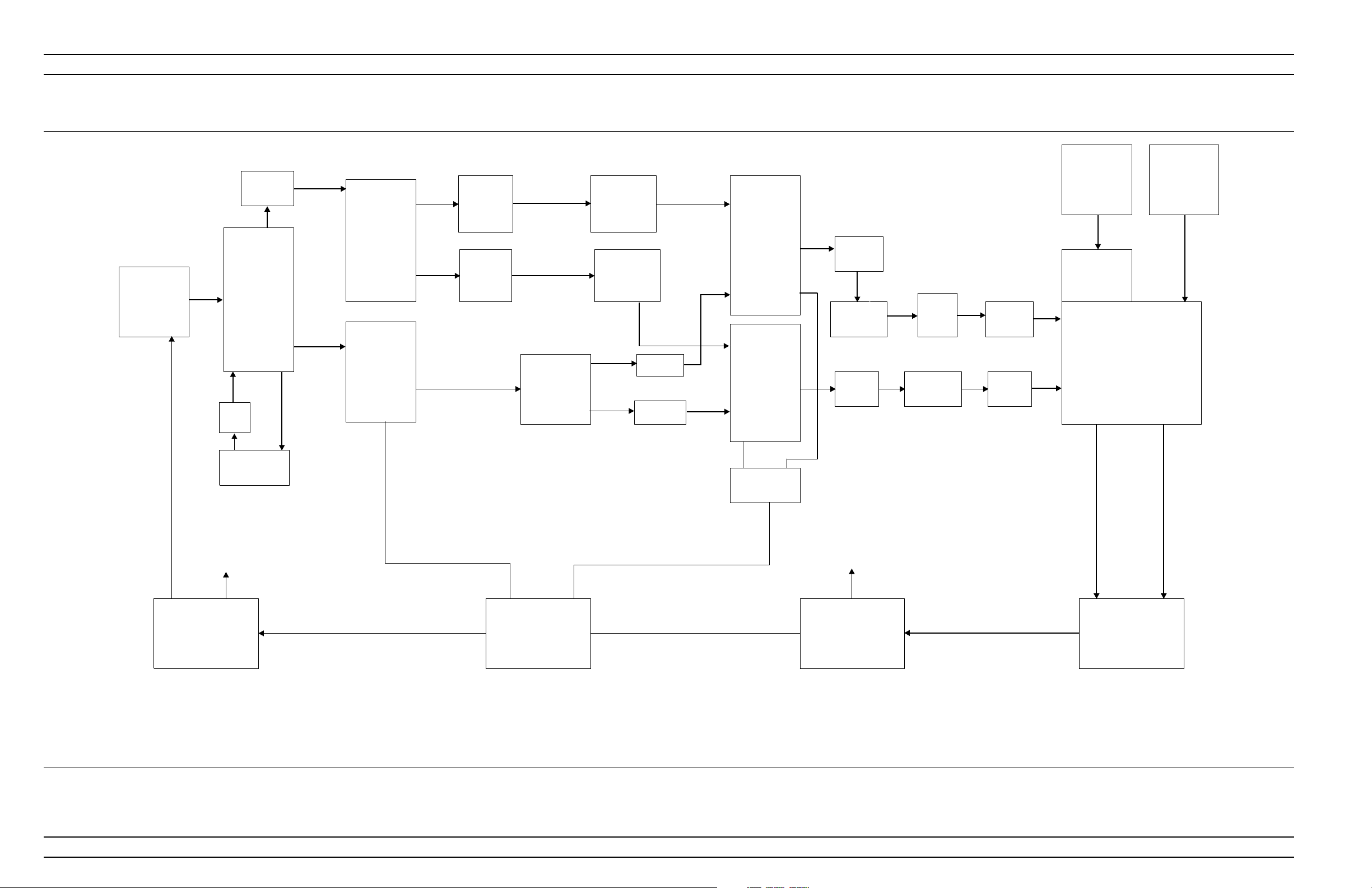
SIGNAL PATHS TROUBLESHOOTING
YIG Oscillator
2-20GHz
Switched Filter
40MHz-
2GHz
15 dB
Pad
Converter
YIG tuning currents
16.8 GHz
Lowpass
Filter
Down
First LO
(A1 PCB)
9.5-
16.25GHz
J4
40MHz-
19GHz
J5
6.3-
8.3GHz
SPDT Switch
X2
(SDM)
Ref A
J3
J2
Ref B
40MHz-38GHz
X4
(SQM)
Forward
X4
(SQM)
Reverse
Ref A 38-65 GHz
Ref B 38-65 GHz
Transfer Switch
(Ref A/ Ref B
Control)
37 GHz
HiPass Filter
37 GHz
HiPass Filter
Ref B
38-65
GHz
J5
Ref A 40MHz - 38GHz
Ref B 40MHz - 38GHz
Ref A 38-65 GHz
3dBpad
3dBpad
J1
MUX Coupler
(forward)
J4
J1
MUX Coupler
(reverse)
J4J4
DCV
ALC Control PCB
49808-3
40MHz-65GHz (Ref A)
J5
DCV
Shaped Pad
J5
40MHz -
65GHz (Ref B)
3dBPad
3dBpad
Rear
Panel
Access
Loop **
Shaped Pad
3dBPad
3dBpad
(357-536MHz)
Power Amp
Sampler/Buffer Amp
J5 J3
Ref A
2.5 MHz CW
Second LO
(A2 PCB)
(25-272MHz)
J1
Ref B
Bias Voltages to YIG,
Switched Filter
Down Converter, SAM
A21A1 PCB
SDM Control
Digital and Analog Control
A21A2 PCB
DC
voltage
J3
J1
DC voltage (6 MHz / Volt)
Control of SPDT
switch, transfer switch,
buffer amp, power
amp, ALC control
A8 PCB
Source Lock/ RF
Component Control
J8
J2J1
2.5 MHz CW
J4
A4 PCB
Reference IF Processor
J7
NOTE: Sampler/Buffer amplifiers are individually matched to
Power Amplifiers. If either fails, both should be replaced with
another matched set, part number ND53249.
** Indicates notpresent on model 37297B or 37277B
Figure 5-4. 37397A Source Lock Signal Path Diagram
5-26 373XXA MM
Page 81

Contents
6-1 INTRODUCTION ·························6-3
6-2 LO1 CALIBRATION························6-3
6-3 LO 2 CALIBRATION ·······················6-4
6-4 FREQUENCY CALIBRATION ··················6-5
Chapter 6 Adjustments
Calibration Procedure ·······················6-3
Post Calibration Actions······················6-3
Calibration Procedure ·······················6-4
Post Calibration Actions······················6-5
Calibration Procedure ·······················6-6
Post Calibration Actions······················6-7
6-5 RF POWER/ALC CALIBRATION·················6-8
Calibration Procedure ·······················6-9
Post Calibration Actions ·····················6-10
6-6 SOURCE LOCK THRESHOLD ·················6-11
Calibration Procedure ······················6-12
Post Calibration Actions ·····················6-12
6-7 A8 ADJUSTMENT (37397A) ··················6-13
Calibration Procedure ······················6-13
Post Calibration Actions ·····················6-13
6-8 A21A2 ADJUSTMENT (37397A) ················6-14
Calibration Procedure ······················6-14
Post Calibration Actions ·····················6-15
Page 82

Page 83

Chapter 6
Adjustments
6-1 INTRODUCTION This chapter contains procedures that are used to restore the calibration
of the 373XXA signal source and the related source lock system assem
blies. Use these procedures after various signal source related assemblies
have been replaced due to troubleshooting or repair activities.
-
Please insure you have read and fully understand the servicing con
cepts for the 373XXApresented in Chapter 1 prior to continuing with
this chapter.
6-2 LO1 CALIBRATION This procedure uses the 373XXA internal diagnostics and calibration
menus to adjust the A1 1st LO PCB assembly. Perform this calibation
procedure if:
The A1 PCB is replaced.
q
q BBRAM chip on A9 Processor PCB is replaced and the Source
Lock Threshold Calibration data was not previously saved on
disk (that is, data is not available for recall from a floppy disk).
Calibration
Procedure
Perform the following steps:
Equipment Required
None
NOTE
Allow the 373XXAto warm-up at least 30 minutes prior to
performing calibration.
Procedure
-
Step 1. Press the Option Menu key (Enhancement key group) to dis
play the OPTIONS menu.
Post Calibration
Actions
Step 2.
Step 3. Follow the directions displayed on the 373XXA CRT screen,
After the calibration process is completed, perform the following ac
tions, as appropriate:
Select DIAGNOSTICS from menu.Then select in se
quence: H/W CALIBRATIONS then LO1 CALIBRA
TION.
until calibration is completed.
-
-
-
373XXA MM 6-3
-
Page 84

LO 2 CALIBRATION ADJUSTMENTS
If calibration passes:
Save the calibration data to (hard) disk, as follows:
Step 1. Press the Option Menu key (Enhancement key group) to dis
play the OPTIONS menu.
Step 2.
If calibration fails:
Step 1. Repeat the calibration. If it still fails, then proceed to
Select DIAGNOSTICS from menu.Then select in se
quence: H/W CALIBRATIONS |DISK OPERATIONS
|SAVE TO HARD DISK|HW_CAL.LO1.
NOTE
Also save the calibration data to floppy disk
for archival purposes as a backup in case of
a hard disk failure. Label the disk with cali
bration type, date, and system model and se
rial numbers. Set the copy protect tab on the
disk. Properly safeguard the disk so that it
will be available for later use, as needed.
Chapter 5, Troubleshooting.
-
-
-
6-3 LO 2 CALIBRATION This procedure uses the 373XXA internal diagnostics and calibration
menus to adjust the A2 2nd LO PCB assembly. Perform this calibation
procedure if:
-
q
The A2 PCB is replaced.
q
BBRAM chip on A9 Processor PCB is replaced and the LO2 Cali
bration data was not previously saved on disk (that is, data is not
available for recall from a floppy disk).
Calibration
Procedure
Perform the following steps:
Equipment Required
None
NOTE
Allow the 373XXAto warm-up at least 30 minutes prior to
performing calibration.
Procedure
Step 1. Press the Option Menu key (Enhancement key group) to dis
play the OPTIONS menu.
6-4 373XXA MM
-
-
Page 85

ADJUSTMENTS FREQUENCY CALIBRATION
Post Calibration
Actions
Step 2.
Step 3. Follow the directions displayed on the 373XXA CRT screen,
After the calibration process is completed, perform the following ac
tions, as appropriate:
If calibration passes:
Save the calibration data to (hard) disk, as follows:
Step 1. Press the Option Menu key (Enhancement key group) to dis
Step 2.
Select DIAGNOSTICS from menu.Then select in se
quence: H/W CALIBRATIONS then LO2 CALIBRA
TION.
until calibration is completed.
play the OPTIONS menu.
Select DIAGNOSTICS from menu.Then select in se
quence: H/W CALIBRATIONS |DISK OPERATIONS
|SAVE TO HARD DISK|HW_CAL.LO2.
NOTE
Also save the calibration data to floppy disk
for archival purposes as a backup in case of
a hard disk failure. Label the disk with calibration type date, and system model and serial numbers. Set the copy protect tab on the
disk. Properly safeguard the disk so that it
will be available for later use, as needed.
-
-
-
-
-
If calibration fails:
Step 1. Repeat the calibration. If it still fails, then proceed to
Chapter 5, Troubleshooting.
6-4 FREQUENCY
CALIBRATION
This procedure uses the internal 373XXA diagnostics and calibration
menus, in conjunction with a suitable frequency counter ,to adjust the sig
nal source frequencies throughout the range of the 373XXA model being
calibrated. Perform this calibration procedure if:
q
The Source FM/Lock Linearity test in Chapter 3, Operational
Test, fails.
q
Other testing or troubleshooting reveals a possible problem with
the signal source frequency accuracy or phase lock loop.
q
Any of the following assemblies are replaced:
n
A21A1 Source YIG/Bias
n
A21A2 Source Controller
n
Down Converter
373XXA MM 6-5
-
Page 86

FREQUENCY CALIBRATION ADJUSTMENTS
YIG Oscillator
n
Switched Filter
n
BBRAM chip on the A9 Processor PCB is replaced and the
q
Source Calibration Data was not previously saved on disk (thus
data could not be recalled from disk).
Calibration
Procedure
Perform the following steps:
Equipment Required
Refer to Table 1-1, located on page 1-9, for further information about
the following equipment:
EIP Model 578B Frequency Counter, or equivalent.
RF/Microwave Cable
GPIB cable, WILTRON 2100-2, or equivalent
NOTE
Allow the 373XXAand Frequency Counter to warm-up at
least 30 minutes prior to performing calibration.
Procedure
Step 1. Press the Option Menu key (Enhancement key group) to dis-
play the OPTIONS menu.
Step 2.
Select DIAGNOSTICS from menu; then select in se
quence: H/W CALIBRATION,and then SOURCE
FREQUENCY CALIBRATION (below).
OPTIONS
TRIGGERS
REAR PANEL
OUTPUT
DIAGNOSTICS
MULTIPLE SOURCE
CONTROL
PRESS <ENTER> TO
SELECT
DIAGNOSTICS
START SELF TEST
READ SERVICE LOG
INSTALLED OPTIONS
PERIPHERAL TESTS
TROUBLESHOOTING
(FOR SERVICE
ONLY)
H/W CALIBRATIONS
(FOR SERVICE
ONLY)
PRESS <ENTER> TO
SELECT
HARDWARE
CALIBRATIONS
(FOR SERVICE
ONLY)
LO1
CALIBRATION
LO2
CALIBRATION
SOURCE FREQUENCY
CALIBRATION
SOURCE ALC
CALIBRATION
DISK OPERATIONS
PREVIOUS MENU
PRESS <ENTER> TO
SELECT
HARDWARE
CALIBRATIONS
(FOR SERVICE
ONLY)
START ALC
FREQ CALIBRATION
PREVIOUS MENU
PRESS <ENTER> TO
SELECT
6-6 373XXA MM
Page 87
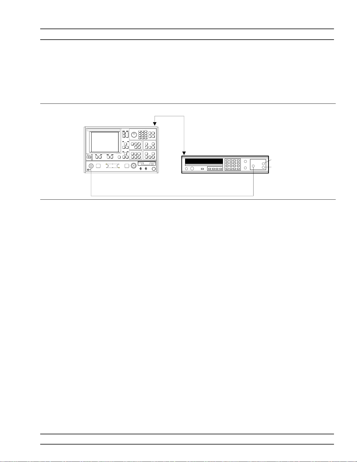
ADJUSTMENTS FREQUENCY CALIBRATION
Step 3. Follow the directions displayed on the screen to set-up and
connect the frequency counter to the 373XXA. Refer also to
373XXA VNA
Dedicated GPIB
789
456
12
3
.
-
0
Figure 6-1 Select START SOURCE FREQ CALIBRA
TION from menu (above).
-
Microwave Cable
Figure 6-1. Test Setup for Frequency Calibration
Step 4. Follow the directions displayed on the 373XXA CRT screen,
Post Calibration
Actions
After the calibration process is completed, perform the following actions, as appropriate:
If calibration passes:
Save the calibration data to (hard) disk, as follows:
Step 1. Press the Option Menu key (Enhancement key group) to dis
Step 2.
EIP 578B Frequency Counter
EIP
Band 1
Band 2
Band 3
until calibration is completed.
play the OPTIONS menu.
Select DIAGNOSTICS from menu.Then select in se
-
quence: H/W CALIBRATIONS |DISK OPERATIONS
|SAVE TO HARD DISK |HW_CAL.FRE.
-
NOTE
Also save the calibration data to floppy disk
for archival purposes as a backup in case of
a hard disk failure. Label the disk with cali
bration type (FRE), date, and system model
and serial numbers. Set the copy protect tab
on the disk. Properly safeguard the disk so
that it will be available for later use, as
needed.
Perform the Source FM/Lock Linearity test in Chapter 3, Operational
Tests. If the test fails, proceed to Chapter 5, Troubleshooting.
373XXA MM 6-7
Page 88

RF POWER/ALC CALIBRATION ADJUSTMENTS
If calibration fails:
6-5 RF POWER/ALC
CALIBRATION
Verify the GPIB cable is connected to the Dedicated GPIB (bot
q
-
tom) connector on the 373XXA rear panel.
Verify that the frequency counter is functioning correctly, the ca
q
ble is in good condition, and all connections are secure.
Note which calibration step failed from the screen messages.
q
Repeat the calibration. If it still fails, then go to Chapter 5, Trou
q
bleshooting.
This procedure uses the 373XXA internal diagnostics and calibration
menus, in conjunction with a suitable power meter, to adjust the out
put power level of the signal source throughout the range of the
373XXA model being calibrated. Perform this calibration procedure if:
The Source Power/ALC test in Chapter 3, Operating Test, fails.
q
Other testing or troubleshooting reveals a possible problem with
q
RF Power accuracy or the ALC loop.
Any of the following assemblies are replaced:
q
n A21A1 Source YIG/Bias
n A21A2 Source Controller
n Down Converter
-
-
-
n YIG Oscillator
n Switched Filter
n
Transfer Switch
n
SDM (37369A)
n
Coupler (37325A and above)
n
Bridge (37317A and below)
n
Port 1 Source Step Attenuator
n
Buffer Amplifier
q
BBRAM chip on the A9 Processor PCB is replaced and the
Source Calibration Data was not previously saved on disk (thus
data could not be recalled from disk).
6-8 373XXA MM
Page 89

ADJUSTMENTS RF POWER/ALC CALIBRATION
Calibration
Procedure
Perform the following steps:
Equipment Required
Refer to Table 1-1, located on page 1-9, for further information about
the following equipment:
HP 437B Power Meter with HP 8487A Power Sensor
or:
ANRITSU ML24XXA with Version 2.02 or later, with ANRITSU
Power Sensors MA2474Aand SC6230 for 50 and 65 GHz units.
or:
Gigatronics 8541/8542 with 80304APower Sensor
GPIB cable, WILTRON 2100-2, or equivalent
NOTE
Allow the 373XXAand power meter to warm-up at least 30
minutes prior to performing calibration.
65 GHz Power Sensor Setup Procedure
The Anritsu SC6230 Power Sensor has an internal frequency calibration factors table. The ML24XX meter settings must be changed so
that the table will be used for frequencies above 50 GHz. To configure
the meter for the new calibration factors table, proceed as follows:
Step 1.
Step 2.
Step 3.
Step 4.
Step 5. Press the System key to exit.
Procedure
Step 1. Press the Option Menu key (Enhancement key group) to
Step 2.
Press the Sensor key then Cal Factor softkey.
Press the More softkey.
Press the Use Table sofkey. Cursor will start blinking.
Press 1 then the Enter softkey.
display the OPTIONS menu.
Select DIAGNOSTICS from menu; then select in se
-
373XXA MM 6-9
Page 90

RF POWER/ALC CALIBRATION ADJUSTMENTS
Dedicated GPIB
ANRITSU 373XXA
VNA
789
6
45
12
3
0.-
SC6230 Sensor
Figure 6-2. Equipment Set-Up for RF Power/ALC Calibration
quence: H/W CALIBRATIONS, and then SOURCE ALC
CALIBRATION (below).
ANRITSU ML24XXA
Power Meter
OPTIONS
TRIGGERS
REAR PANEL
OUTPUT
DIAGNOSTICS
MULTIPLE SOURCE
CONTROL
PRESS <ENTER> TO
SELECT
DIAGNOSTICS
START SELF TEST
READ SERVICE LOG
INSTALLED OPTIONS
PERIPHERAL TESTS
TROUBLESHOOTING
(FOR SERVICE
ONLY)
H/W CALIBRATIONS
(FOR SERVICE
ONLY)
PRESS <ENTER> TO
SELECT
HARDWARE
CALIBRATIONS
(FOR SERVICE
ONLY)
LO1
CALIBRATION
LO2
CALIBRATION
SOURCE FREQUENCY
CALIBRATION
SOURCE ALC
CALIBRATION
DISK OPERATIONS
PREVIOUS MENU
PRESS <ENTER> TO
SELECT
Set-Up
HARDWARE
CALIBRATIONS
(FOR SERVICE
ONLY)
START SOURCE
FREQ CALIBRATION
PREVIOUS MENU
PRESS <ENTER> TO
SELECT
Step 3. Follow the directions displayed on the screen to set-up and
connect the power meter to the 373XXA. Refer also to Fig
ure 6-2. Select START ALC CALIBRATION from menu.
Step 4. Follow the directions displayed on the 373XXA CRT screen,
until calibration is completed.
Step 5. If the software allows a Port 2 ALC Calibration, perform it
now.
-
Post Calibration
Actions
After the calibration process is completed, perform the following ac
tions, as appropriate:
-
6-10 373XXA MM
Page 91

ADJUSTMENTS SOURCE LOCK THRESHOLD
If calibration passes:
Save the calibration data to (hard) disk, as follows:
Step 1. Press the Option Menu key (Enhancement key group) to dis
play the OPTIONS menu.
Step 2.
Select DIAGNOSTICS from menu.Then select in se
-
quence: H/W CALIBRATIONS |DISK OPERATIONS
|SAVE TO HARD DISK|HW_CAL.ALC.
NOTE
Also save the calibration data to floppy disk
for archival purposes as a backup in case of
a hard disk failure. Label the disk with cali
bration type (ALC), date, and system model
and serial numbers. Set the copy protect tab
on the disk. Properly safeguard the disk so
that it will be available for later use, as
needed.
Perform the RF Power Generation and Control test in Chapter 3, Operational Tests. If the test fails, proceed to Chapter 5, Troubleshooting.
If calibration fails:
q
Verify the GPIB cable is connected to the Dedicated GPIB (bottom) connector on the 373XXA rear panel.
-
6-6 SOURCE LOCK
THRESHOLD
Calibration
Procedure
q
Verify that the power meter and sensor are functioning correctly,
the cables are in good condition, and all connections are secure.
q
Verify the correct power sensor data exists in the power meter.
q
Note the failed step in the calibration procedure from the screen
messages.
q
Repeat calibration. If it still fails then proceed to Chapter 5,
Troubleshooting.
This procedure uses the 373XXA internal diagnostics and calibration
menus to adjust the source lock threshold of the phase-lock loop. Per
form this calibation procedure if:
q
The A4 PCB is replaced.
q
BBRAM chip on A9 Processor PCB is replaced and the Source
Lock Threshold Calibration data was not previously saved on
disk (that is, data is not available for recall from a floppy disk).
Perform the following steps:
-
373XXA MM 6-11
Page 92

SOURCE LOCK THRESHOLD ADJUSTMENTS
Equipment Required
None
NOTE
Allow the 373XXAto warm-up at least 30 minutes prior to
performing calibration, and perform the ALC calibration
(paragraph 6-3) before doing this calibration.
Procedure
Step 1. If recalibrating a 37397A , install broadband terminations
to both ports or install a throughline between ports.
Post Calibration
Actions
Step 2. Press the Option Menu key (Enhancement key group) to dis
play the OPTIONS menu.
Step 3.
Step 4. Follow the directions displayed on the 373XXA CRT screen,
After the calibration process is completed, perform the following actions, as appropriate:
If calibration passes:
Save the calibration data to (hard) disk, as follows:
Step 1. Press the Option Menu key (Enhancement key group) to dis
Step 2.
Select DIAGNOSTICS from menu.Then select in se
quence: H/W CALIBRATIONS then SOURCE THRESH
OLD CALIBRATION.
until calibration is completed.
play the OPTIONS menu.
Select DIAGNOSTICS from menu.Then select in se
quence: H/W CALIBRATIONS |DISK OPERATIONS
|SAVE TO HARD DISK|HW_CAL.SLT.
NOTE
Also save the calibration data to floppy disk
for archival purposes as a backup in case of
a hard disk failure. Label the disk with cali
bration type, date, and system model and se
rial numbers. Set the copy protect tab on the
disk. Properly safeguard the disk so that it
will be available for later use, as needed.
-
-
-
-
-
-
-
If calibration fails:
q
Repeat the calibration. If it still fails, then proceed to Chapter 5,
Troubleshooting.
6-12 373XXA MM
Page 93

ADJUSTMENTS A8 ADJUSTMENT (37397A)
6-7 A8 ADJUSTMENT
(37397A)
Calibration
Procedure
The adjustments are important to the operation of the VNA above 56
GHz. Improperly adjusted A8 Potentiometers may cause lock failures.
Perform these adjustments as follows:
The A8 PCB is replaced.
q
44733 Buffer Amp is replaced.
q
Perform the following steps:
Equipment Required
None
NOTE
Allow the 373XXAto warm-up at least 30 minutes prior to
performing calibration, and perform the ALC calibration
(paragraph 6-3) before doing this calibration.
Procedure
Step 1. Connect a V Throughline (3670V50-2 with FF Adapter) be-
tween Ports 1 and 2.
Step 2. Set the 373XXA to sweep from 50 to 65 GHz.
Post Calibration
Actions
Step 3. Set RF power to 0 dB (default value).
Step 4. Using Diagnostics menu, view Non-Ratio parameters.
Step 5. View Channel 1 (Ref A) only, and activate Autoscale.
Step 6. Adjust the “RA” potentiometer on top of A8 for the flattest
trace display. A small discontinuity at 56 GHz is normal.
Step 7. Perform Step 6 for each of the four Non-Ratio channels.
After the calibration process is completed, perform the following ac
tions, as appropriate:
If calibration passes:
Save the calibration data to (hard) disk, as follows:
Step 1. Press the Option Menu key (Enhancement key group) to dis
play the OPTIONS menu.
Step 2.
Select DIAGNOSTICS from menu.Then select in se
quence: H/W CALIBRATIONS |DISK OPERATIONS
|SAVE TO HARD DISK|HW_CAL.SLT.
-
-
-
373XXA MM 6-13
Page 94

A21A2 ADJUSTMENT (37397A) ADJUSTMENTS
NOTE
Also save the calibration data to floppy disk
for archival purposes as a backup in case of
a hard disk failure. Label the disk with cali
bration type, date, and system model and se
rial numbers. Set the copy protect tab on the
disk. Properly safeguard the disk so that it
will be available for later use, as needed.
If calibration fails:
Repeat the calibration. If it still fails, then proceed to Chapter 5,
q
Troubleshooting.
-
-
6-8 A21A2 ADJUSTMENT
(37397A)
Calibration
Procedure
This adjustment ensures the correct RF power level will be available
to drive the source quadrupler modules (SQMs). Perform these adjust
ments as follows:
D454244 is replaced.
q
A21A2 PCB is replaced.
q
C21620 YIG Oscillator is replaced.
q
NOTE
Failure to perform this adjustment may result in intermittent operation.
Perform the following steps:
Refer to Table 1-1, located on page 1-9, for further information about
the following equipment:
HP 437B Power Meter with HP 8487A Power Sensor
or:
ANRITSU ML24XXA with Version 2.02 or later, with ANRITSU
Power Sensors MA2474Aand SC6230 for 50 and 65 GHz units.
-
or:
Gigatronics 8541/8542 with 80304APower Sensor
GPIB cable, WILTRON 2100-2, or equivalent
NOTE
Allow the 373XXAand power meter to warm-up at least 30
minutes prior to performing calibration.
6-14 373XXA MM
Page 95

ADJUSTMENTS A21A2 ADJUSTMENT (37397A)
Procedure
Step 1. With power off and the new part installed, disconnect the
RF cable from J4 of the Switched Filter.
Step 2. Install Power Sensor (usea6or10dBpadforprotection)
to Switched Filter J4.
Step 3. Turn on the 373XXA and set it to 38 GHz, CW.
Step 4. Adjust A21A2R238 for maximum power, but not over +26
dBm.
Step 5. Remove the pad and sensor and reconnect the RF cable to
J4.
Post Calibration
Actions
Step 6. Perform the procedures in paragraph 6-4 and 6-5 (fre
quency and ALC calibrations).
After the calibration process is completed, perform the following ac-
tions, as appropriate:
If calibration passes:
Save the calibration data to (hard) disk, as follows:
Step 1. Press the Option Menu key (Enhancement key group) to dis-
play the OPTIONS menu.
Step 2.
Select DIAGNOSTICS from menu.Then select in se-
quence: H/W CALIBRATIONS |DISK OPERATIONS
|SAVE TO HARD DISK|HW_CAL.SLT.
NOTE
Also save the calibration data to floppy disk
for archival purposes as a backup in case of
a hard disk failure. Label the disk with cali
bration type, date, and system model and se
rial numbers. Set the copy protect tab on the
disk. Properly safeguard the disk so that it
will be available for later use, as needed.
-
-
-
If calibration fails:
Repeat the calibration. If it still fails, then proceed to Chapter 5, Trou
bleshooting.
373XXA MM 6-15
-
Page 96

Chapter 7 System Description
Table of Contents
7-1 INTRODUCTION ·························7-3
7-2 SYSTEM OVERVIEW ·······················7-3
7-3 ANALOG SUBSYSTEM ASSEMBLIES ·············7-7
Signal Source Module ·······················7-7
Test Set Module ··························7-8
A7PCB, 10 MHz Timebase ···················7-9
Receiver Module ·························7-10
A8, Source Lock/ Signal Separation and Control PCB ·····7-11
IF Section ·····························7-11
A7PCB,LO3··························7-12
A5 A/D Converter PCB······················7-12
7-4 DIGITALSUBSYSTEM ASSEMBLIES·············7-13
A9 Main Processor PCB Assembly················7-13
A13 I/O Interface #1 PCB Assembly···············7-15
A14 I/O Interface #2 PCB Assembly···············7-15
A15 Graphics Processor PCB Assembly ·············7-16
A16 Hard Disk PCB Assembly··················7-16
Floppy Disk Drive Assembly···················7-16
A24 VME Bus Terminator PCB ·················7-16
7-5 MAIN CHASSIS ASSEMBLIES·················7-16
A17 System Motherboard Assembly···············7-16
Front Panel Assembly ······················7-16
Rear Panel Assembly·······················7-17
A18 Rear Panel Interface PCB··················7-17
Power Supply Module ······················7-18
Internal VGA Monitor ······················7-19
Page 97

Page 98

Chapter 7
System Description
7-1 INTRODUCTION This chapter provides a brief overview of the functional assemblies
and major parts that comprise a typical Series 373XXA VNAsystem.
It also briefly describes the operation of each major assembly.
7-2 SYSTEM OVERVIEW Series 373XXAVector Network Analyzers are ratio measurement sys
tems used to measure complex vector signal characteristics (real/imagi
nary, magnitude/phase, etc) of devices and systems in the 22.5 MHz to
65 GHz frequency range.
The 373XXA performs these measurements by sourcing a stimulus sig
nal to the Device Under Test (DUT) that is connected to the front
panel Port 1 and/or Port2 connectors. (See Figure 7-1 on page 7-5). It
simultaneously measures the DUT response, which consists of reflected and/or transmitted (attenuated, or amplified) signals at the
connectors of the DUT. The reflected and/or transmitted signal(s) and
a sample of the stimulus signal, are down converted and then transformed into their real and imaginary vector components. The resultant vector components are measured and converted into digital information. This digital information is sent to the Main Processor PCB
where the desired S-parameter data is normalized and then presented
to the user via the front panel color display. The display information is
also sent to the rear panel VGA Out connector for use with an external
VGA monitor.
The normalized measurement information is also sent to the rear
panel Printer Out connector for use with an external printer and/or
plotter.
A front panel keypad, a rotary knob, and an IBM compatible keyboard
interface provide user interaction with 373XXA Main Processor PCB.
-
-
-
The system is equipped with internal hard disk and floppy disk drives
and battery backed internal memories for storage and retrieval of data
and front panel setup information.
The 373XXA implements an IEEE 488.2 interface. This GPIB inter
face allows an externally connected instrument controller to control
the 373XXA system in the “Remote-Only” mode. All 373XXAmeasure
ment and input/output operations may be controlled remotely in this
mode.
-
373XXA MM 7-3
-
Page 99

SYSTEM OVERVIEW SYSTEM DESCRIPTION
An internal service log stores a record of system failures, data about
the failures, and other key system service information. The service log
is implemented using internal battery-backed SRAM memory.
7-4 373XXA MM
Page 100

SYSTEM DESCRIPTION SYSTEM OVERVIEW
bias tee
PORT 1
bias tee
PORT 2
FP Amp Loop
DOWN
CONV
SIGNAL SOURCE
Step Attenuator
0-70dB
Step Attenuator
µP
YIG OSC
2-20 GHz
YIG
SWITCHED
0-40dB
DOUBLER
FILTER
SDM
2X
LOCK
DET
ALC
µP
b Loop
1
F
R
F
R
LVL
DET
LVL
DET
a Loop
1
TEST SET MODULE**
*
b
1
*
a
1
*
a
2
*
b
2
QUAD
SAMPLER/BUFFER
S
S
S
S
HARM
GEN
L.O.
#1
L.O.
#2
L.O.
#3
IF / SYNC/ DET
EXTERNAL
KEYBOARD
FLTR / S/H / A/D
S
D
S
D
S
D
S/H
S/H
S/H
S/H
ANALOG
MUX
S/H
S/H
TO ANALOG PCB'S
(CTL & DATA)
A/D
CTL
QUIET BUS
HARD
DISK
DRIVE
FLOPPY
DISK
DRIVE
FRONT
PANEL
PCB
A/D BUS
MAIN PROCESSOR PCB
µP
68030
RAM
INTERFACE
CTL
BBRAM
VME BUS
GRAPHICS
PROCESSOR
PCB
INTERNAL
VGA
MONITOR
EXT VGA MONITOR
REAR
PANEL
PCB
R.P.
LOGIC
CKTS
GPIB
INTERFACE
A/D BUS
INTERFACE
&
CONTROL
EXTERNAL
KEYBOARD
INTERFACE
FRONT
PANEL
INTERFACE
I/O PCB'S
FLOPPY
DISK DRIVE
CONTROL
VME
INTERFACE
I/O CONTROL
LOGIC
REAR PANEL
INTERFACE
&
CONTROL
* pad values:
37347B and below 20dB 6db
37369B 6dB
** For Models 37377A and 37397A, see Figures 5-3 and 5-4
a channels b channels
3db
REF OSC
10 MHz
QUIET BUS
INTERFACE
&
CONTROL
*Model 37369A only
Figure 7-1. Overall Block Digram of 373XXA VNA System
373XXA MM 7-5
 Loading...