Evaluation Board User Guide
UG-162
One Technology Way • P. O . Box 9106 • Norwood, MA 02062-9106, U.S.A. • Tel : 781.329.4700 • Fax : 781.461.3113 • www.analog.com
CDMA Evaluation Board For PLL Frequency Synthesizer
FEATURES
Self-contained evaluation board that includes a synthesizer,
VCO, and loop filter for generating CDMA frequencies
(824 MHz to 849 MHz)
Designed for 3 kHz loop bandwidth
Accompanying software allows complete control of
synthesizer functions from a PC
Battery operated: choice of 3 V or 5 V supply
Typical phase noise performance of −81 dBc/Hz at 300 Hz offset
Typical spurious performance of better than −81 dBc at
30 kHz offset from carrier
FUNCTIONAL BLOCK DIAGRAM
GENERAL DESCRIPTION
The EVAL-ADF4112EBZ1 evaluation board is designed to evaluate
the performance of the ADF4112 frequency synthesizer for phase
locked loops (PLLs). Figure 1 is the functional block diagram of
the board and shows the ADF4112 frequency synthesizer, a PC
connector, an SMA connector for the reference input, the power
supplies, and an RF output. There is also a loop filter (3 kHz bandwidth) and a voltage controlled oscillator (VCO) incorporated
on the board. A cable is included in the evaluation board package
to connect the evaluation board to a PC printer port.
The evaluation board package contains Windows® based software
to allow easy programming of the ADF4112 frequency synthesizer.
TCXO
9V BATTERY
POWER SWITCH
ON OFF
FILTER
ADF411x
EVAL-ADF41 12EBZ1
PC CONNECTOR
Figure 1.
V
P
MUXOUT
CE
9147-001
V
DD
V
VCO
TES T
SMA
SOCKET
VCO
TEST
RF
OUT
REF
IN
PLEASE SEE THE LAST PAGE FOR AN IMPORTANT
WARNING AND LEGAL TERMS AND CONDITIONS.
Rev. 0 | Page 1 of 8

UG-162 Evaluation Board User Guide
TABLE OF CONTENTS
Features.............................................................................................. 1
General Description ......................................................................... 1
Functional Block Diagram .............................................................. 1
Revision History ............................................................................... 2
Evaluation Board Hardware............................................................ 3
REVISION HISTORY
7/11—Revision 0: Initial Version
Evaluation Board Software...............................................................4
Installing the Software..................................................................4
Using the Software ........................................................................4
Evaluation Board Schematics...........................................................5
Rev. 0 | Page 2 of 8

Evaluation Board User Guide UG-162
C
A
EVALUATION BOARD HARDWARE
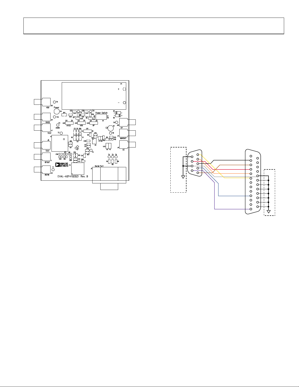
The evaluation board package includes a cable for connecting
the EVAL-ADF4112EBZ1 to the printer port of a PC. The
silkscreen and cable diagram for the evaluation board are
shown in Figure 2 and Figure 3. The board schematics are
shown in Figure 5 and Figure 6.
09147-002
NOTES:
1. THE VALUES FOR LOOP COMPONENTS ARE AS FOLLOWS:
1 = 4.7nF, C2 = 47nF, C3 = 620pF, R1 = 5.1kΩ, R2 = 22kΩ.
Figure 2. Evaluation Board Silkscreen
The evaluation board is powered from a single 9 V battery. The
power supply circuitry allows the user to individually choose either
3 V or 5 V for the V
of the ADF4112, the VP of the ADF4112,
DD
and the supply of the VCO. The default settings are 3 V for the
V
of the ADF4112 and 5 V for the VP of the ADF4112 and for
DD
the supply of the VCO.
It is important to note that the V
exceed the V
of the ADF4112 because damage to the device
P
of the ADF4112 should never
DD
may result.
The EVAL-ADF4112EBZ1 includes all the components required
for LO generation. A 13 MHz temperature compensated crystal
oscillator (TCXO) from Vectron International, Inc., provides the
necessary reference input. The PLL comprises the ADF4112
frequency synthesizer, the passive loop filter (20 kHz bandwidth),
and the VCO (190-836T from Vari-L Company, Inc.). The output
is available at RFOUT through a standard SMA connector. A
different reference input and different power supplies can be
used, if desired. In this case, insert SMA connectors as shown in
the silkscreen (Figure 2) and cable diagram (Figure 3).
DF4112EBZ1
1
6
2
7
3
8
4
9
5
Figure 3. PC Cable Diagram
BLACK—CLK
BROWN—DATA
RED—LE
ORANGE—CE
WHITE—GND
YELLOW
BLUE
PURPLE
1
14
2
15
3
16
4
17
5
18
6
19
7
20
8
21
9
22
10
23
11
24
12
25
13
PC
Rev. 0 | Page 3 of 8
 Loading...