

Page 1
Software User Guide
V
UG-005
One Technology Way • P. O . Box 9106 • Norwood, MA 02062-9106, U.S.A. • Tel : 781.329.4700 • Fax : 781.461.3113 • www.analog.com
ADP8860 Software User Guide
INTRODUCTION
This user guide describes the functionality of the Analog
Devices, Inc., ADP8860 and provides software development
guidelines. The ADP8860 communicates with an external
processor using an I
2
C interface and an interrupt line (nINT).
The processor sends initialization and activation commands
to the ADP8860, which acts as a slave device.
The interrupt line, from the ADP8860 to the processor, is used
to indicate a failure condition, such as a thermal shutdown or
an overvoltage and LED/output short circuit, or to indicate a
V
OUT
light level threshold has been crossed. All interrupt sources are
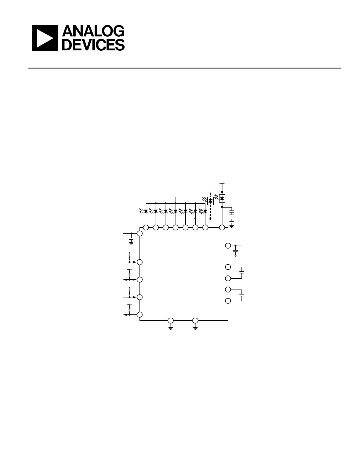
maskable. Refer to Figure 1 for a typical application diagram.
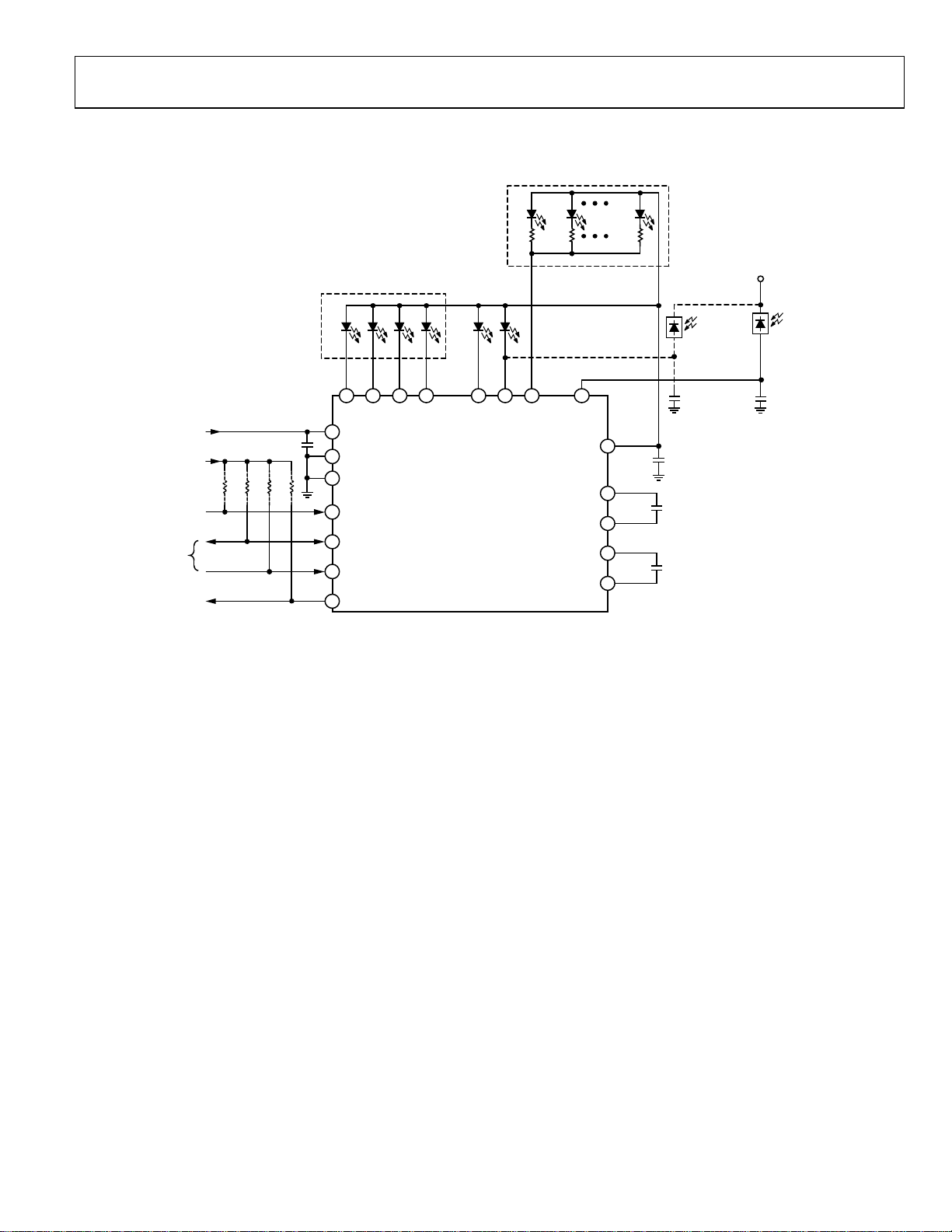
Figure 2 shows a schematic with keypad light control.
The interrupt line is active low; each interrupt source has an
individual masking bit. The processor can reset the ADP8860
anytime by pulling the nRST line low; this operation reinitializes the ADP8860 at the default state and places the device
in standby mode.
OPTIONAL
PHOTOSENSOR
ALS
PHOTOSENSOR
0.1µF
0.1µF
V
A2
A1
C1
B1
B2
C1+
C1–
C2+
C2–
1µF
OUT
C1
1µF
C2
1µF
08158-001
V
nRST
SDA
SCL
nINT
IN
1µF
VDDIO
VDDIO
VDDIO
VDDIO
D3D1E3D2E4D3D4D4C4D5B4
A3
E1
ADP8860
C2
E2
D2
A4
GND1
D6/
CMP_IN2
D1
GND2
D7C3CMP_IN
B3
Figure 1. Typical Application Schematic with Optional Second Photo Diode
Rev. 0 | Page 1 of 44
Page 2

UG-005 Software User Guide
TABLE OF CONTENTS
ADP8860 Software User Guide ...................................................... 1
Introduction ...................................................................................... 1
Revision History ............................................................................... 2
I2C Interface Mode ........................................................................... 4
Interrupts ........................................................................................... 5
Data Flow Diagrams ......................................................................... 6
Setting the LED Current .................................................................. 8
Fade Override Mode .................................................................. 14
Setting Backlight and Sink Timings ............................................. 15
Controlling Backlight Settings .................................................. 15
REVISION HISTORY
7/09—Revision 0: Initial Version
Controlling Sink Settings .......................................................... 15
Light Sensing Comparator ............................................................ 17
Conventions .................................................................................... 19
Functional Flowcharts ................................................................... 20
Registers Map .................................................................................. 30
Pseudocode Implementation ........................................................ 31
Listing for ADP8860_Regs.h .................................................... 31
Listing for ADP8860 Constants.h ............................................ 36
Listing for ADP8860 Reset.h .................................................... 38
Listing for ADP8860 MainProgram.c...................................... 39
Rev. 0 | Page 2 of 44
Page 3
Software User Guide UG-005
KEYPAD LIGHT
UP TO 10 LEDs (6mA EACH)
60mA MAX TOTAL CURRENT
VDDIO
I
CONTRO L
SIGNALS
V
IN
R1 R2 R3 R4
nRST
2
C
nINT
1µF
DISPLAY BACKLI GHT
DL1
DL2
DL3
D3
E3
D1
VIN
A3
GND1
A4
D1
GND2
nRST
E1
SDA
C2
SCL
E2
nINT
D2
E4
D2
D3
Figure 2. Schematic with Keypad Light Control
DL4
D4
D4
ACCESSORY
LIGHTS OR
SUB-DISPLAY BL
DL5
DL6
C4
B4
D5
D6/
CMP_IN2
ADP8860
DL7R5DL8
R6
B3
D7C3CMP_IN
VOUT
C1+
C1–
C2+
C2–
DL17
R15
2.8V
PH2
OPTIONAL
PHOTOSENSOR
0.1µF
A2
A1
C1
B1
B2
1µF
C1
1µF
C2
1µF
PH1
MAIN
PHOTOSENSOR
0.1µF
08158-002
Rev. 0 | Page 3 of 44
Page 4
UG-005 Software User Guide
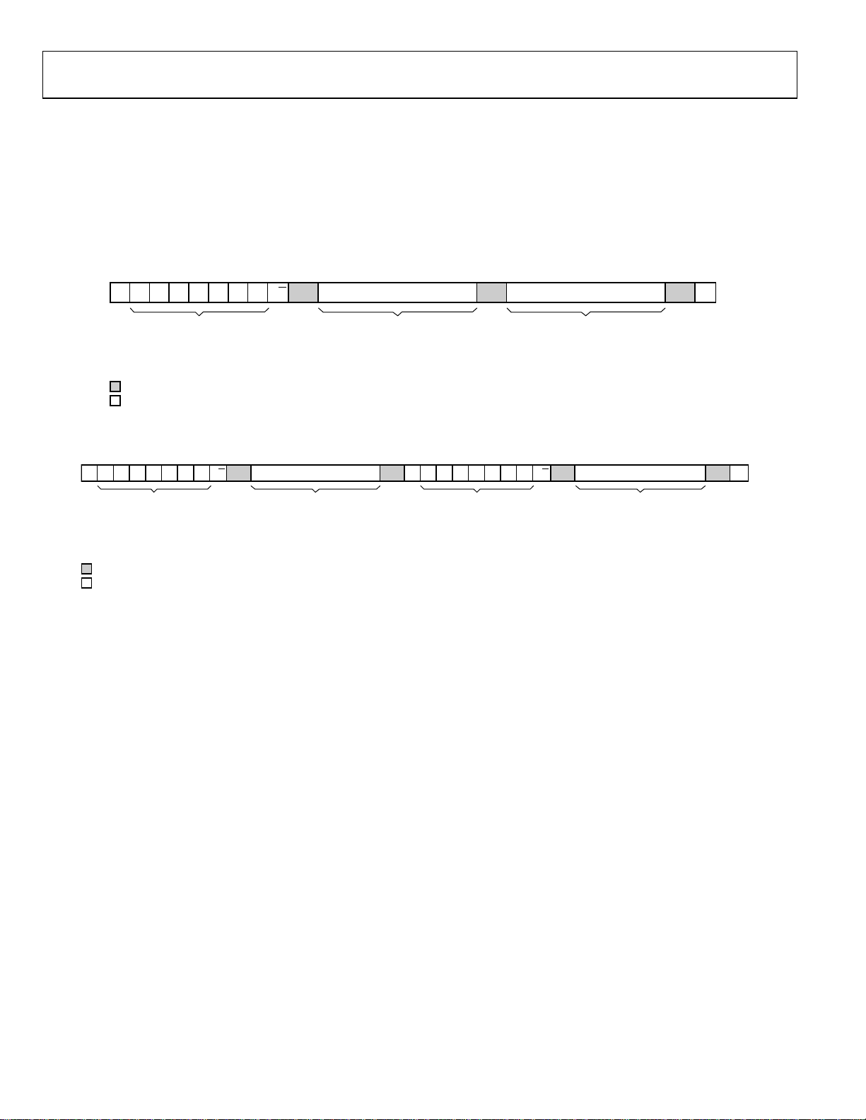
I2C INTERFACE MODE
The ADP8860 includes an I2C-compatible serial interface for
controlling the LED current, as well as for readback of system
status registers. The I
2
C device address is 0x54 (0101 0100,
binary) for a write sequence and 0x55 (0101 0101, binary) for
a read sequence. Figure 3 shows the I
2
C write sequence while
Figure 4 shows a read operation.
B7 B0 B7 B0 B7 B0
ST ACK REGISTER ADDRESS ACK REGISTER VALUE
0101010
R/W
The ADP8860 sends data from the register denoted by the
register address. The lowest bit number (0) represents the least
significant bit, and the highest bit number (7) represents the
most significant bit. The register address content selects which
of the ADP8860 registers data is written to or read from.
ACK
ST
START
SLAVE TO MASTER
MASTER TO SLAVE
DEVICE ID
0x54 FOR WRI TE
OPERATIO N
SELECT ADP8860 REGISTER TO
WRITE I N THE 0x00 TO 0x24 AND
WRITE = 0
FROM ADP8860
0x2E RANGE
Figure 3. I
2
C Write Operation
8-BIT VALUE TO WRITE IN THE
ADDRESSED REGIST ER
FROM ADP8860
FROM ADP8860
STOP
08158-003
B7 B0 B7 B0 B7 B0
ST
DEVICE ID
0x54 FOR WRI TE
START
OPERATION
SLAVE TO MASTER
MASTER TO SLAVE
R/W
ACK REGISTER ADDRESS ACK ACK REGISTER VALUE ACK0101010
SELECT ADP8860 REGISTER TO
WRITE I N THE 0x00 TO 0x24 AND
WRITE = 0
FROM ADP8860
0x2E RANGE
Figure 4. I
B7 B0
RS0101010
DEVICE ID
0x55 FOR READ
OPERATION
FROM ADP8860
REPEATED START
2
C Read Operation
R/W
8-BIT VALUE TO WRITE IN THE
READ = 1
ADDRESSED REGIST ER
FROM MASTER
ST
STOP
08158-004
Rev. 0 | Page 4 of 44
Page 5
Software User Guide UG-005
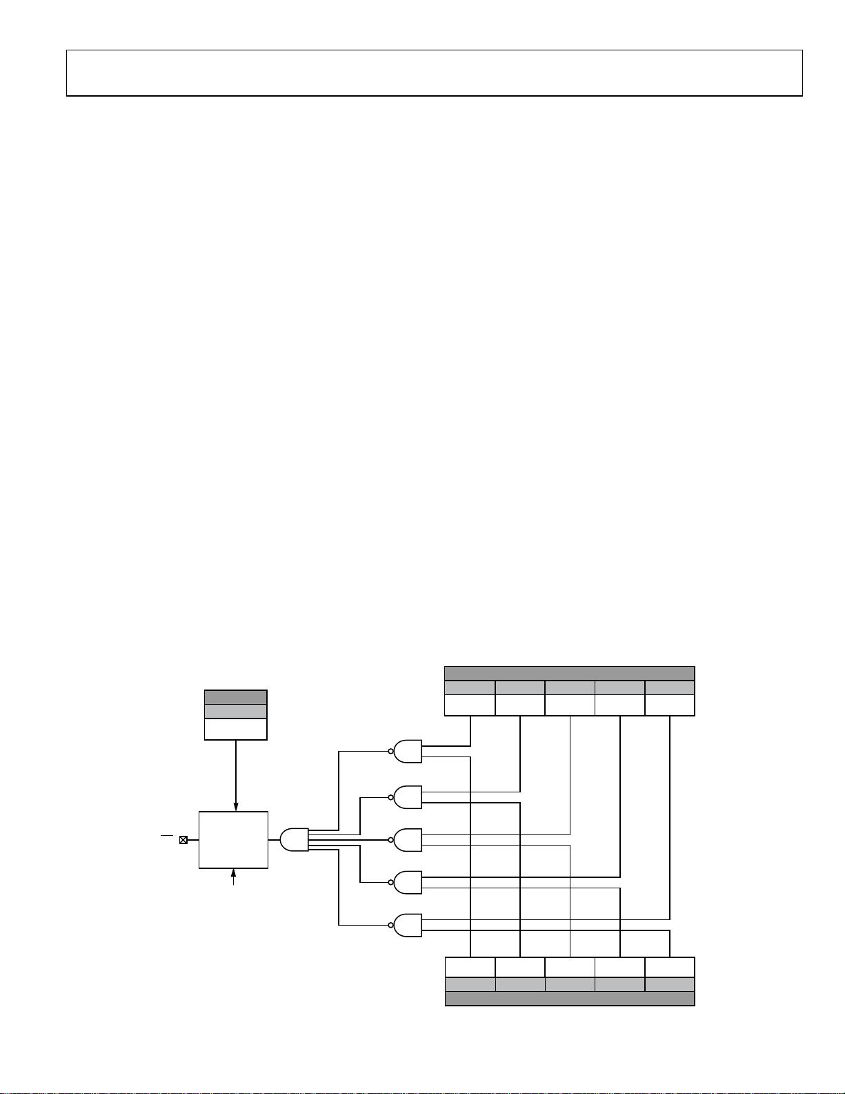
INTERRUPTS
There are up to five interrupt sources available on the ADP8860
as follows:
• CMP_INT is from the main light sensor comparator.
• CMP2_INT is from sensor Comparator 2.
• OVP_INT is from the overvoltage protection comparator.
• TSD_INT is from the thermal shutdown circuit.
• SHORT_INT is from the short-circuit detection
comparator.
Each interrupt has individual masking/enable bits mapped in
Register INTR_EN. If the respective bit in the masking register
is 0, an interrupt is not generated to the external processor,
however the interrupt pending bit (on the MDCR2 register) can
be set in case the monitored condition occurs. This can be used
by the processor to periodically poll the interrupt pending
register (Register MDCR2) looking for an event to be true. If
the masking register bit is 1 an interrupt is generated (the nINT
line goes low) to the external processor in case an interrupt
pending bit is set.
CMP_INT is set every time the main light sensor comparator
detects a threshold transition (rising or falling condition). This
comparator has two programmable thresholds (L2 and L3)
defining the transition level from dark to office (L3) and from
office to outdoor (L2).
The CMP2_INT interrupt works the same way as CMP_INT
except that the sensing input comes from the second light
sensor. The programmable threshold is the same as the main
light sensor comparator.
The OVP_INT interrupt is generated when the charge pump
output voltage rises above a safety limit. In the event of an over-
voltage condition, the charge-pump is disabled until the output
voltage decreases to a recovery working level. An overvoltage
event can be generated when the load is removed from the
circuit and the input voltage, multiplied by the charge pump
gain (can be 1.5× or 2×), is above the OVP limit. In this condition, the interrupt to the external processor is generated
periodically. Therefore, the software should handle a case of
this sort by turning off the ADP8860 or disabling the OVP
interrupt mask.
The TSD_INT interrupt is generated when the die temperature in
the ADP8860 rises above a safety limit, typically 150°. When this
condition occurs, the charge pump and the LED drivers are turned
off waiting for the die to cool down. When the die temperature
decreases below ~130° the circuit is activated again automatically.
No interrupt is generated when the device turns on again, however
if the software clears the pending interrupt and the temperature
remains above 130° another interrupt is generated.
The SHORT_INT interrupt is generated if the output of the
charge-pump VOUT is shorted to ground or an LED connected
to the sink output is shorted. In a short-circuit event, the charge
pump and drivers are turned off immediately and the shortcircuit pending flag is set. The processor may then retry new
activations or issue a diagnostic message. Interrupts are cleared
by writing a 1 in the pending register bit. If Bit INT_CFG in
Register MDCR is set to 1, this forces the nINT line deassertion
(Logic High) for 50 μs after the processor clears the interrupt
pending, and the interrupt condition persists. If INT_CFG is 0,
the nINT line remains asserted (Logic Low) after the processor
clears the interrupt pending and the interrupt condition
persists.
MDCR (0x01)
BIT 6
INT_CFG
50µs
INT
INTERRUPT
DE-ASSERTI ON
INT_CLEAR
(ASSERTED WHEN WRITING
THE INTERRUPT PENDING
FLAGS I N MDCR2)
BIT 4 BIT 3 BIT 2 BIT 1 BIT 0
SHORT_IEN CMP_IENCMP2_IENOVP_IENTSD_IEN
SHORT_INT TSD_INT OVP_INT CMP2_INT CMP_INT
BIT 4 BIT 3 BIT 2 BIT 1 BIT 0
Figure 5. Interrupt Logic
Rev. 0 | Page 5 of 44
INTR_EN (0x03) – INTERRUPT MASKS
MCDR2 (0x02) – INT ERRUPT PENDING
08158-005
Page 6
UG-005 Software User Guide
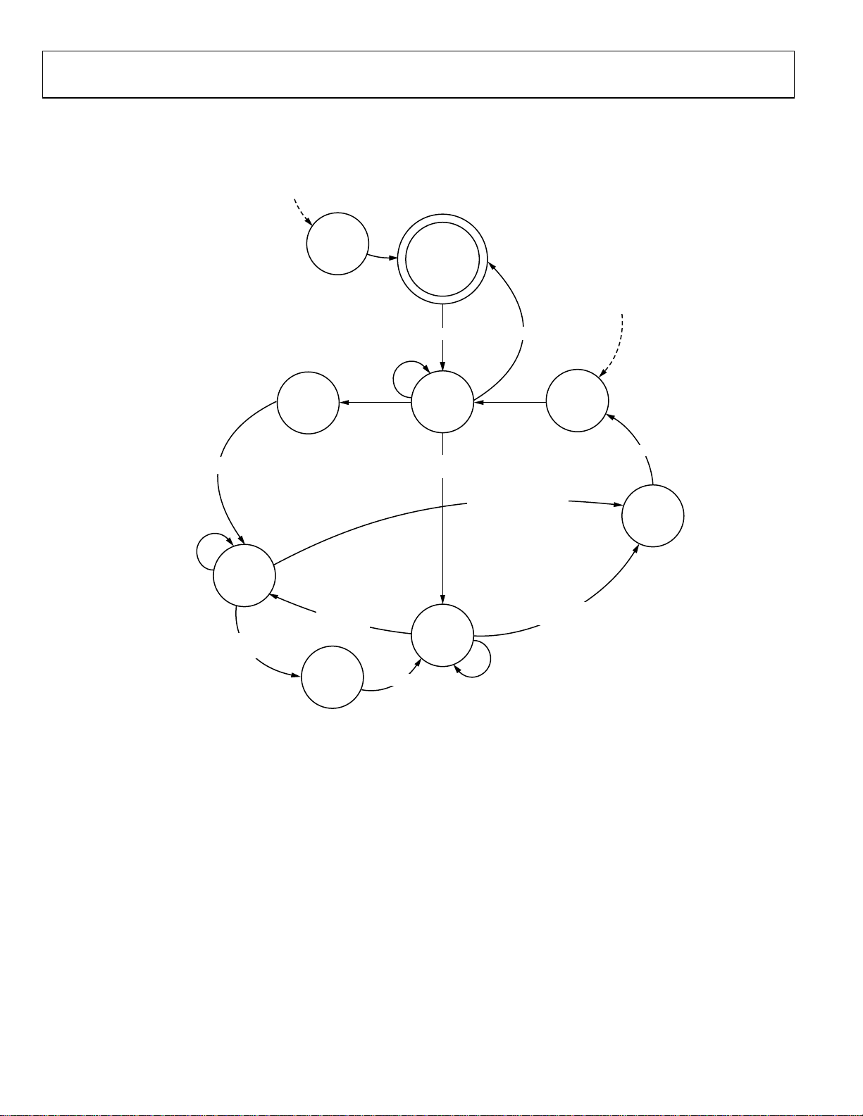
DATA FLOW DIAGRAMS
Figure 6 and Figure 7 show the backlight data flow and the individual data flow, respectively.
NSTBY = 0
OR VIN < UVLO
TURN OFF
BACKLIGHT
AND ISINKS
STANDBY
BLEN = 0
OR TSD_INT = 1
OR SHORT_INT = 1
NSTBY = 1
NO COMMAND
BLEN AND
FOVR = 1
FADE IN
TO DIM
BLEN = 1
BL_FO TIMEOUT
WAITING
COMMAND
DIM_EN AND
BLEN = 1
BACKLIGHT
DIM STATE
(OFFT)
BACKLIGHT
FADE IN
TO MAX
BL_FI TIMEOUT
DIMT = DISABL ED
BACKLIGHT
ACTIVATIO N
TIME (DIMT)
DIM_EN = 1
AND DIMT TIM EOUT
BACKLIGHT
NOTES
1. DASHED LINE INDICATES AN INTERRUPT O R AN EVENT THAT CAN HAPPEN ANYTI ME DURING THE DEVICE O PERATION.
2. COMMANDS FRO M I
COMMANDS TO MAKE THE FLOW REPRES ENTATION CLEARER.
2
C ARE ALWAYS MO NITORED AND EXECUTED. T HE FLOW SHOWS A COMMON BUBBLE FOR
NSTBY = 0
DIM_EN = 0
AND DIMT = DISABL ED
OFFT TIMEOUT
AND DIM_EN = 0
DIM_EN = 1 OR
OFFT = DISABLED
BACKLIGHT
OFF
BL_FO TIMEOUT
BACKLIGHT
FADE OUT
Figure 6. Backlight Data Flow
TO OFF
08158-006
Rev. 0 | Page 6 of 44
Page 7
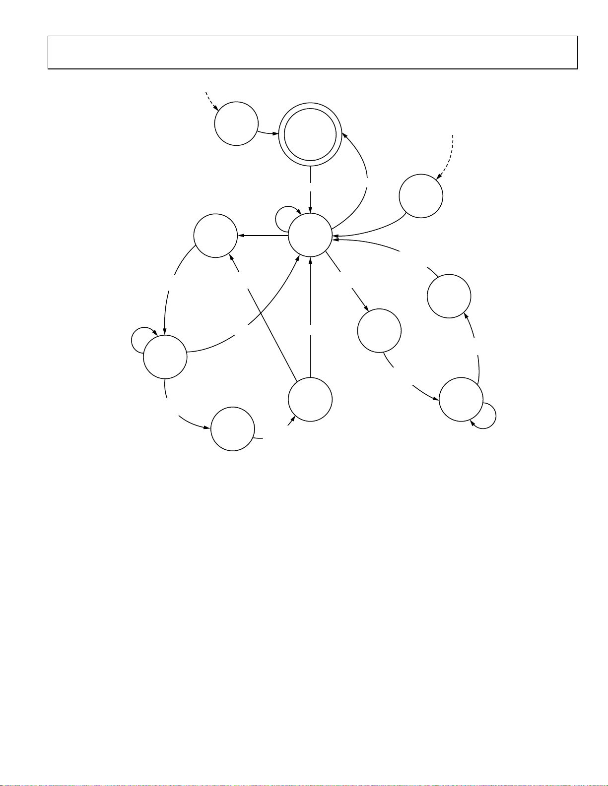
Software User Guide UG-005
OR TIMEOUT
SCx OFF = 0
(ALWAYS ON)
ACTIVATIO N
INDIVIDUAL
xSINK
TIMEOUT
SCFI = 0
SCON
NSTBY = 0
OR VIN < UVLO
BACKLIGHT
AND ISINKS
xSINK
FADE-IN
FADE-OUT
TURN OFF
STANDBY
NSTBY = 1
NO COMMAND
WAITING
SCx_EN = 1
SCx OFF
TIMEOUT
SCx_EN = 0 SCx_EN = 0
xSINK
COMMAND
TURN OFF
INDIVIDUAL
SCFO = 0
OR TIMEOUT
SINK
NSTBY = 0
SIS_EN = 1
AND ISCC = 0
ENABLED
SINKS
FADE-IN
OR TIMEOUT
xSINK
SCFO = 0
OR TIMEOUT
SCFI = 0
SCx_EN = 0
OR TSD_INT = 1
OR SHORT_INT = 1
OFF
ENABLED
SINKS
FADE-OUT
ACTIVATE
ENABLED
SIS_EN = 0
OR ISCC ≠ 0
SINKS
SIS_EN = 1
AND ISCC = 0
NOTES
1. DASHED LINE INDICATES AN INTERRUPT O R AN EVENT THAT CAN HAPPEN ANYTI ME DURING THE DEVICE OPERATION.
Figure 7. Individual Sinks Data Flow
Rev. 0 | Page 7 of 44
08158-007
Page 8
UG-005 Software User Guide
SETTING THE LED CURRENT
The ADP8860 contains seven current sink outputs that can be
software configured to operate as part of the LED backlight or
as individual sinks, such as funlights or keypad lights. All
outputs can drive up to 30 mA with the exception of the seventh
sink (D1B/LED7) that can drive up to 60 mA, which is ideal for
keypad light applications where up to 10 LEDs can be driven in
parallel with shunt resistors (see Figure 2).
The application software must program which output to use as
part of the backlight and which to use for the individual sinks.
Register BLSEN is used for this purpose. If the selection bit
associated with the LED sink (Bit 0 controls LED1, Bit 1
controls LED2, and so on) is set to 0, it is part of the LED
backlight; otherwise, if set to 1, it is an independent sink. In
this case, Register ISCC controls the individual sink turn-on
and turn-off activations. For example, if BLSEN is programmed
with 0x70, LED1 to LED4 are used for the backlight while LED5
to LED7 are individual sinks. Bit 7 in BLSEN is not used.
In backlight operation, there are three distinct selectable brightness levels: dark, office, and daylight. Each brightness level has
two programmable settings:
• The MAX brightness defined in Register BLMX1 (day-
light), Register BLMX2 (office), and Register BLMX3
(dark) can range from 0 mA to 30 mA.
• The DIM brightness level defined in Register BLDM1 for
daylight, Register BLDM2 for office, and Register BLDM3
for dark can range from 0 mA to 30 mA.
The backlight LED current depends on the backlight transfer
law, linear or square, programmed in the CFGR register Bit 2
and Bit 1. Tabl e 2 shows all the current values available
according to the control law selected.
The transfer function for the linear law is
__
ISCALEFULL
⎞
⎟
⎠
RegValue
⎛
_
RegValueIBACKLIGHT (1)
= (2)
×=
⎜
⎝
IBACKLIGHT
127_ ×
ISCALEFULL
__
127
where:
BACKLIGHT_I is the desired LED current in mA.
RegValue is the digital 7-bit value programmed in the backlight
current registers.
FULL_SCALE_I is the maximum backlight current value, which
is 30 mA.
The transfer function for the square law is
2
⎞
__Re
ISCALEFULLgValue
(3)
⎟
⎟
⎠
RegValue
⎛
⎜
_
=
IBACKLIGHT
⎜
⎝
=
×
127
IBACKLIGHT
_127 ×
(4)
ISCALEFULL
__
Table 1. Backlight Transfer Laws—CFGR Register Bits[2:1]
Bits[2:1] Fading Law Fading Time Change
00 Linear Law DAC Linear time steps
01 Square Law DAC Linear time steps
10
11
Square Law DAC
(Cubic 1)
Square Law DAC
(Cubic 2)
Nonlinear time steps
(Type 1)
Nonlinear time steps
(Type 2)
The complete set of square law current values are given in
Tabl e 2.
Rev. 0 | Page 8 of 44
Page 9

Software User Guide UG-005
Table 2. Linear and Square Law Current Values
DAC Code Linear Law (mA) Square Law (mA)
0x00 0 0.000
0x01 0.236 0.002
0x02 0.472 0.007
0x03 0.709 0.017
0x04 0.945 0.030
0x05 1.181 0.047
0x06 1.417 0.067
0x07 1.654 0.091
0x08 1.890 0.119
0x09 2.126 0.151
0x0A 2.362 0.186
0x0B 2.598 0.225
0x0C 2.835 0.268
0x0D 3.071 0.314
0x0E 3.307 0.365
0x0F 3.543 0.419
0x10 3.780 0.476
0x11 4.016 0.538
0x12 4.252 0.603
0x13 4.488 0.671
0x14 4.724 0.744
0x15 4.961 0.820
0x16 5.197 0.900
0x17 5.433 0.984
0x18 5.669 1.071
0x19 5.906 1.163
0x1A 6.142 1.257
0x1B 6.378 1.356
0x1C 6.614 1.458
0x1D 6.850 1.564
0x1E 7.087 1.674
0x1F 7.323 1.787
0x20 7.559 1.905
0x21 7.795 2.026
0x22 8.031 2.150
0x23 8.268 2.279
0x24 8.504 2.411
0x25 8.740 2.546
0x26 8.976 2.686
0x27 9.213 2.829
0x28 9.449 2.976
0x29 9.685 3.127
0x2A 9.921 3.281
0x2B 10.157 3.439
0x2C 10.394 3.601
0x2D 10.630 3.767
0x2E 10.866 3.936
0x2F 11.102 4.109
DAC Code Linear Law (mA) Square Law (mA)
0x30 11.339 4.285
0x31 11.575 4.466
0x32 11.811 4.650
0x33 12.047 4.838
0x34 12.283 5.029
0x35 12.520 5.225
0x36 12.756 5.424
0x37 12.992 5.627
0x38 13.228 5.833
0x39 13.465 6.043
0x3A 13.701 6.257
0x3B 13.937 6.475
0x3C 14.173 6.696
0x3D 14.409 6.921
0x3E 14.646 7.150
0x3F 14.882 7.382
0x40 15.118 7.619
0x41 15.354 7.859
0x42 15.591 8.102
0x43 15.827 8.350
0x44 16.063 8.601
0x45 16.299 8.855
0x46 16.535 9.114
0x47 16.772 9.376
0x48 17.008 9.642
0x49 17.244 9.912
0x4A 17.480 10.185
0x4B 17.717 10.463
0x4C 17.953 10.743
0x4D 18.189 11.028
0x4E 18.425 11.316
0x4F 18.661 11.608
0x50 18.898 11.904
0x51 19.134 12.203
0x52 19.370 12.507
0x53 19.606 12.814
0x54 19.842 13.124
0x55 20.079 13.439
0x56 20.315 13.757
0x57 20.551 14.078
0x58 20.787 14.404
0x59 21.024 14.733
0x5A 21.260 15.066
0x5B 21.496 15.403
0x5C 21.732 15.743
0x5D 21.968 16.087
0x5E 22.205 16.435
0x5F 22.441 16.787
Rev. 0 | Page 9 of 44
Page 10

UG-005 Software User Guide
DAC Code Linear Law (mA) Square Law (mA)
0x60 22.677 17.142
0x61 22.913 17.501
0x62 23.150 17.863
0x63 23.386 18.230
0x64 23.622 18.600
0x65 23.858 18.974
0x66 24.094 19.351
0x67 24.331 19.733
0x68 24.567 20.118
0x69 24.803 20.507
0x6A 25.039 20.899
0x6B 25.276 21.295
0x6C 25.512 21.695
0x6D 25.748 22.099
0x6E 25.984 22.506
0x6F 26.220 22.917
DAC Code Linear Law (mA) Square Law (mA)
0x70 26.457 23.332
0x71 26.693 23.750
0x72 26.929 24.173
0x73 27.165 24.599
0x74 27.402 25.028
0x75 27.638 25.462
0x76 27.874 25.899
0x77 28.110 26.340
0x78 28.346 26.784
0x79 28.583 27.232
0x7A 28.819 27.684
0x7B 29.055 28.140
0x7C 29.291 28.599
0x7D 29.528 29.063
0x7E 29.764 29.529
0x7F 30.000 30.000
Rev. 0 | Page 10 of 44
Page 11

Software User Guide UG-005
If the automatic light sensing control is enabled (CMP_AUTOEN,
Bit 1, is set to 1 in Register MDCR) the result from the light
sensing comparator controls the backlight brightness in one of
the three levels (dark, office, and daylight).
In this mode, it is not possible to force, by software, a defined
level. Thus, settings on Bits[4:3] (BLV) in the CFGR register are
not considered in automatic light sensing mode. In case the
automatic light sensing mode is disabled (0 is written to
CMP_AUTOEN in the MDCR register), software can force the
backlight brightness in one of the three possible modes (dark,
office, or daylight) by writing Bits[4:3] (BLV) in Register CFGR
(see Tabl e 3).
Table 3. Brightness Level—Bits[4:3] (BLV) in CFGR Register
Bits[4:3] Backlight Brightness Level
00 Level 1 (daylight)
01 Level 2 (office)
10 Level 3 (dark)
11 Disabled
Each individual sink has a dedicated current register defining
its brightness level. As with the backlight, the current level
depends on the transfer law selected in the ISCFR register
Bits[1:0] (SC_LAW).
The ISC1 register defines the current level for LED1, the ISC2
register defines the level for LED2, and so on until ISC7, which
controls the current for LED7. The maximum current level
programmable is 30 mA. However, LED7 can be set up to
60 mA if Bit 7 in the ISC7 register is set to 1. The possible
current levels for 30 mA are listed in Tab le 2 .
Rev. 0 | Page 11 of 44
Page 12

UG-005 Software User Guide
Table 4. Complete Set of Square Law Current Values for LED7
—60 mA Range
DAC Code Linear Law (mA) Square Law (mA)
0x00 0.000 0
0x01 0.472 0.004
0x02 0.945 0.014
0x03 1.42 0.034
0x04 1.89 0.06
0x05 2.36 0.094
0x06 2.83 0.134
0x07 3.31 0.182
0x08 3.78 0.238
0x09 4.25 0.302
0x0A 4.72 0.372
0x0B 5.20 0.45
0x0C 5.67 0.536
0x0D 6.14 0.628
0x0E 6.61 0.73
0x0F 7.09 0.838
0x10 7.56 0.952
0x11 8.03 1.076
0x12 8.50 1.206
0x13 8.98 1.342
0x14 9.45 1.488
0x15 9.92 1.64
0x16 10.39 1.8
0x17 10.87 1.968
0x18 11.34 2.142
0x19 11.81 2.326
0x1A 12.28 2.514
0x1B 12.76 2.712
0x1C 13.23 2.916
0x1D 13.70 3.128
0x1E 14.17 3.348
0x1F 14.65 3.574
0x20 15.12 3.81
0x21 15.59 4.052
0x22 16.06 4.3
0x23 16.54 4.558
0x24 17.01 4.822
0x25 17.48 5.092
0x26 17.95 5.372
0x27 18.43 5.658
0x28 18.90 5.952
0x29 19.37 6.254
0x2A 19.84 6.562
0x2B 20.31 6.878
0x2C 20.79 7.202
0x2D 21.26 7.534
DAC Code Linear Law (mA) Square Law (mA)
0x2E 21.73 7.872
0x2F 22.20 8.218
0x30 22.68 8.57
0x31 23.15 8.932
0x32 23.62 9.3
0x33 24.09 9.676
0x34 24.57 10.058
0x35 25.04 10.45
0x36 25.51 10.848
0x37 25.98 11.254
0x38 26.46 11.666
0x39 26.93 12.086
0x3A 27.40 12.514
0x3B 27.87 12.95
0x3C 28.35 13.392
0x3D 28.82 13.842
0x3E 29.29 14.3
0x3F 29.76 14.764
0x40 30.24 15.238
0x41 30.71 15.718
0x42 31.18 16.204
0x43 31.65 16.7
0x44 32.13 17.202
0x45 32.60 17.71
0x46 33.07 18.228
0x47 33.54 18.752
0x48 34.02 19.284
0x49 34.49 19.824
0x4A 34.96 20.37
0x4B 35.43 20.926
0x4C 35.91 21.486
0x4D 36.38 22.056
0x4E 36.85 22.632
0x4F 37.32 23.216
0x50 37.80 23.808
0x51 38.27 24.406
0x52 38.74 25.014
0x53 39.21 25.628
0x54 39.69 26.248
0x55 40.16 26.878
0x56 40.63 27.514
0x57 41.10 28.156
0x58 41.57 28.808
0x59 42.05 29.466
0x5A 42.52 30.132
0x5B 42.99 30.806
Rev. 0 | Page 12 of 44
Page 13

Software User Guide UG-005
DAC Code Linear Law (mA) Square Law (mA)
0x5C 43.46 31.486
0x5D 43.94 32.174
0x5E 44.41 32.87
0x5F 44.88 33.574
0x60 45.35 34.284
0x61 45.83 35.002
0x62 46.30 35.726
0x63 46.77 36.46
0x64 47.24 37.2
0x65 47.72 37.948
0x66 48.19 38.702
0x67 48.66 39.466
0x68 49.13 40.236
0x69 49.61 41.014
0x6A 50.08 41.798
0x6B 50.55 42.59
0x6C 51.02 43.39
0x6D 51.50 44.198
DAC Code Linear Law (mA) Square Law (mA)
0x6E 51.97 45.012
0x6F 52.44 45.834
0x70 52.91 46.664
0x71 53.39 47.5
0x72 53.86 48.346
0x73 54.33 49.198
0x74 54.80 50.056
0x75 55.28 50.924
0x76 55.75 51.798
0x77 56.22 52.68
0x78 56.69 53.568
0x79 57.17 54.464
0x7A 57.64 55.368
0x7B 58.11 56.28
0x7C 58.58 57.198
0x7D 59.06 58.126
0x7E 59.53 59.058
0x7F 60 60
Rev. 0 | Page 13 of 44
Page 14
UG-005 Software User Guide
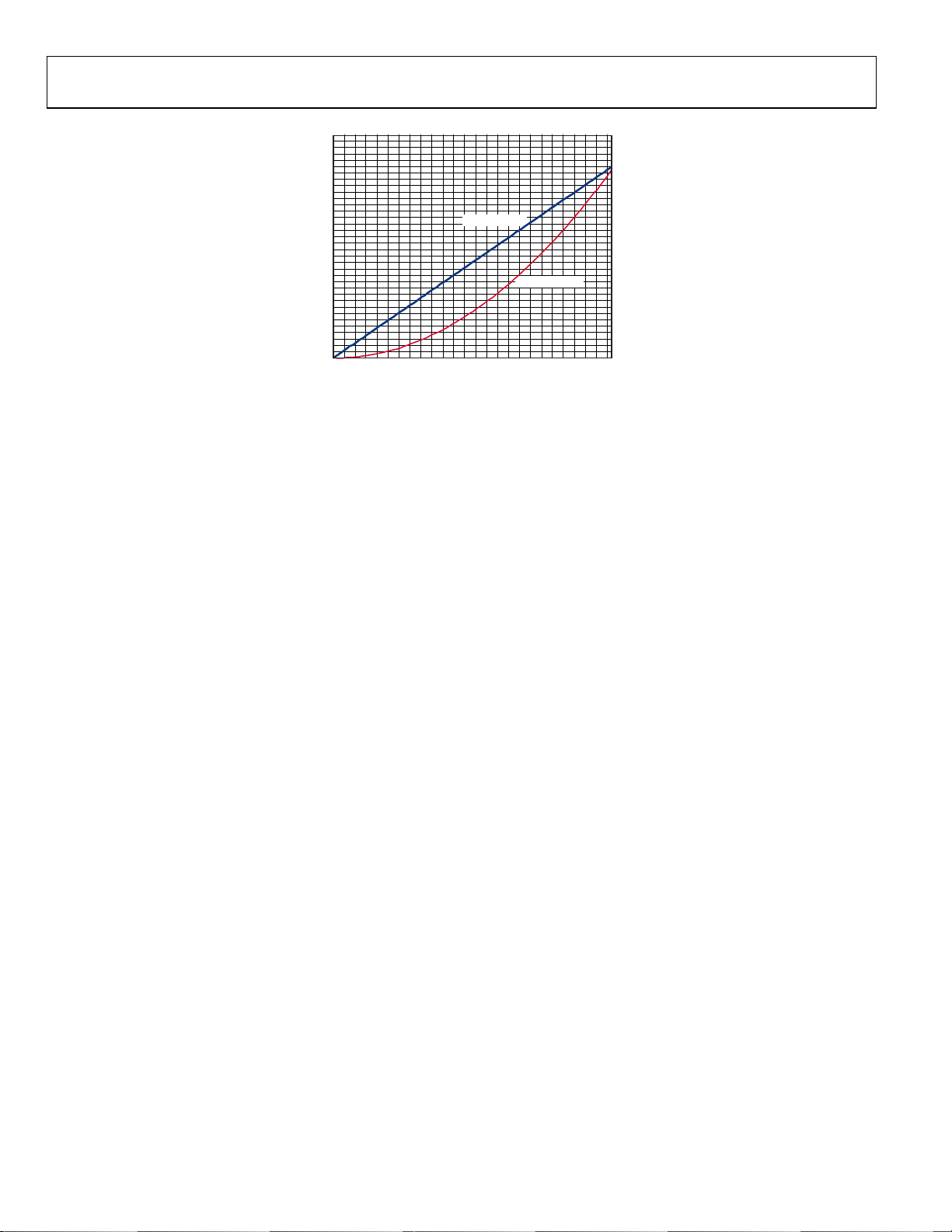
Square Cubic Law 1 and Square Cubic Law 2 use the same
square transfer law values with faster increment/decrement
times when fading in and out.
FADE OVERRIDE MODE
The fade override mode is enabled when Bit 0 (FOVR) in the
CFGR register is set to 1. In this mode, the backlight skips the
fade-in time when Bit BLEN in the MDCR register is set to 1
and it goes directly to the programmed maximum backlight
35
30
25
20
15
LED CURRENT (mA)
10
5
0
0 20 40 60 80 100 120
Figure 8. LED Current Transfer Law Curves
LINEAR LAW
SQUARE LAW
DIGITAL VALUE (DAC)
brightness intensity. There remains a 100 ms ramp-up time to
avoid rapid change in current. The fade-in time is not skipped
at the very first activation, after an off condition.
This mode is useful is situations where the backlight is fading
out and the user depresses a keypad button. The system
software can intercept this condition, set the FOVR bit, then
write the BLEN bit to 1 again. Fade-out time is not affected by
the FOVR bit.
08158-008
Rev. 0 | Page 14 of 44
Page 15

Software User Guide UG-005
SETTING BACKLIGHT AND SINK TIMINGS
The LED backlight supports several programmable timing
controls as described in this section.
Note that the following equation is only for linear step control
laws:
CONTROLLING BACKLIGHT SETTINGS
Bits[3:0] of the BLFR register set the backlight fade-in time (see
Tabl e 5). The time specified in Ta ble 5 is from the maximum
allowable current level (30 mA) to zero. Equation 5 gives an
estimated value for the actual fade-in time based on known
conditions. If the value programmed is zero, the fade-in time is
disabled, however a 100 ms fade-in time is used.
Bits[7:4] of the BLFR register set the backlight fade-out time,
(see Tabl e 5). Equation 6 gives an estimated value for the actual
fade-in time based on known conditions. If the value programmed is zero, the fade-out time is disabled, however a 100 ms
fade-in time is used.
Bits[6:0] of the BLDIM register set the time for the backlight
to stay in the MAX brightness state. After this time, the backlight starts to fade out to the DIM or zero level (If the DIM
timeout is disabled). The digital value programmed in this
register corresponds to the time in seconds. For example,
BLDIM = 0x32 corresponds to 50 seconds.
Bits[6:0] of the BLOFF register set the time for the backlight
to stay in the DIM state. After this time, the backlight starts to
fade out to zero current level. The digital value programmed in
this register corresponds to the time in seconds. For example,
BLOFF = 0x10 corresponds to 16 seconds.
Table 5. Backlight Fade-In (Bits[3:0]) and Fade-Out
(Bits[7:4]) Times
BLFR Register Value Fade-In and Fade-Out Time (Sec)
0000 Disabled
0001 0.3
0010 0.6
0011 0.9
0100 1.2
0101 1.5
0110 1.8
0111 2.1
1000 2.4
1001 2.7
1010 3.0
1011 3.5
1100 4.0
1101 4.5
1110 5.0
1111 5.5
ActualCurrMaxCurrInFade
T
= (5)
_
ESTFADE
−×
30
)(_
where:
MaxCurr is the maximum backlight current value programmed
in the BLMXx registers.
ActualCurr is the initial backlight current (0 mA at the first
activation).
T
is the calculated fade-in time in seconds.
FADE _ES T
Note that the following equation is only for linear step
control laws:
MinCurrActualCurrOutFade
T
= (6)
_
ESTFADE
30
−×
)(_
where:
ActualCurr is the backlight current value and can be MaxCurr if
fading out from the MAX brightness state or DimCurr if fading
out from DIM state.
MinCurr is the backlight current value and can be DimCurr if
fading out from the MAX brightness to DIM state or zero if
fading out from DIM state to zero current.
T
is the calculated fade-out time in seconds.
FADE _ES T
CONTROLLING SINK SETTINGS
The enabled individual sinks have dedicated registers to control
the activation timings and fade-in, fade-out times. The activation on time for Sink 1 to Sink 7 is selected by Register ISCT1,
Bits[7:6] and is common for all the individual sinks (see
Tabl e 6).
The off time is selected individually for each individual sink
(Sink 1 to Sink 7) by Register ISCT1, Bits[5:0] and Register
ISCT2, Bits[7:0] (see Table 7). Two bits are used per individual
sink. If the off time, 2-bit register is set to zero, the individual
sink is activated indefinitely.
The off time is controlled on each individual sink as follows:
ISCT1 Bits[5:4] for Sink 7, ISCT1 Bits[3:2] for Sink 6, ISCT1
Bits[1:0] for Sink 5, ISCT2 Bits[7:6] for Sink 4, ISCT2 Bits[5:4]
for Sink 3, ISCT2 Bits[3:2] for Sink 2 and ISCT2 Bits[1:0] for
Sink 1.
Table 6. Individual Sinks On-Time Selection
ISCT1 Bits[7:6] Programmed On Time (Sec)
00 0.2
01 0.6
10 0.8
11 1.2
Rev. 0 | Page 15 of 44
Page 16

UG-005 Software User Guide
Table 7. Individual Sinks Off-Time Selection
Two-Bit Register Programmed Off Time (Sec)
00 Always on
01 0.6
10 1.2
11 1.8
Bits[3:0] of the ISCF register set the individual sinks fade-in
time (see Tab le 8). The time specified in Tabl e 8 is from zero
to the maximum allowable current level (30 mA or 60 mA for
Sink 7). Equation 5 gives an estimated value for the fade-in time
based on the actual programmed LED current. If the value
programmed is zero, the fade-in time is disabled; however, a
100 ms fade-in time is used.
Bits[7:4] of the ISCF register set the individual sinks fade-out
time (see Tab le 8). The time specified in Tabl e 8 is from the
maximum allowable current (30 mA or 60 mA for Sink 7) to
zero current. Equation 6 gives an estimated value for the fadeout time based on actual programmed LED current. If the value
programmed is zero, the fade-out time is disabled; however, a
100 ms fade-in time is used.
Table 8. Individual Sinks Fade-In and Fade-Out Times
Register Value Fade-In and Fade-Out Time in Seconds
0000 Disabled
0001 0.3
0010 0.6
0011 0.9
0100 1.2
0101 1.5
0110 1.8
0111 2.1
1000 2.4
1001 2.7
1010 3.0
1011 3.5
1100 4.0
1101 4.5
1110 5.0
1111 5.5
Rev. 0 | Page 16 of 44
Page 17

Software User Guide UG-005
LIGHT SENSING COMPARATOR
The ADP8860 supports two light sensing inputs. The first light
sensing input is always dedicated as input from a phototransistor assessing the ambient light condition. The second light
sensing input is shared with Sink 6. Thus, the software must
carefully select the desired operation (light sensing or Sink 6).
Bit 5 (CMP2_SEL) in the CFGR register is used to configure pin
D6 (LED6) operation. If CMP2_SEL is 0, Pin D6 is an output
sink for LED6. If CMP2_SEL is set to 1, Pin D6 is an input from
the second light sensor (phototransistor). An internal analogto-digital converter processes the light information coming
from the light sensors providing a digital value corresponding
to the ambient light detected. The digital value is compared to
two thresholds (L2 and L3) to determine if the ambient light
condition is in one of the following three ranges:
Dark: Ambient light level is below L3 and L2 thresholds.
•
•
Office: Ambient light level is above L3, but below L2
thresholds.
•
Daylight: Ambient light level is above L3 and L2
thresholds.
Software can program the ADP8860 to operate in automatic
mode if Bit 1 (CMP_AUTOEN) in the MDCR register is set
to 1 or in manual mode, if CMP_AUTOEN is 0. When the
device operates in automatic light ambient mode, the backlight
brightness level is set by the current ambient light condition
(dark, office, and daylight).
Bit 0 and Bit 1 in CCFG and CCFG2 allow selection of the level
(L2 and/or L3) used for the automatic brightness control. If
both bits are 0, no automatic control is issued (see Table 9 ).
Software must program the desired levels for the L2 and L3
thresholds in the L2_TRP and L3_TRP registers, respectively.
Using the default phototransistor, the correlation factor between
programmed value and light level is provided in Table 10.
Table 9. Comparators Auto Level Control
Code Comparator Operation
00 No automatic brightness control
01 L2 comparator auto level control
10 L3 comparator auto level control
11 L2 and L3 auto level control
Table 10. Correlation Between Code and Phototransistor Lux
Measurement
Threshold Registers 1-Bit Correlation
L2 L2_TRP, L2_HYS 10 lux or 4 μA
L3 L3_TRP, L3_HYS 1.25 lux or 0.5 μA
Each threshold has an associated register setting the hysteresis
level to avoid changes due to noise or being too close to the
threshold. Each light sensor has an individual comparator and
control register.
Tabl e 11 shows the filter settings for the comparators. The
comparator filter makes sure that rapid changes in the ambient
light level do not change the backlight brightness.
Table 11. Comparators Filter Settings—Bits[7:5] in CCFG
and CCFG2
Code Filter Setting (ms)
000 80
001 160
010 320
011 640
100 1280
101 2560
110 5120
111 10240
Every time the L2 or L3 threshold is crossed (rising or falling
conditions), a pending flag is set in the interrupt pending
register (MDCR2). Bit 0 (CMP_INT) is the flag for the first
light sensor while Bit 1 (CMP2_INT) is the flag for the second
light sensor. An interrupt is generated if the respective Interrupt
Enable bit is 1 in the INTR_EN register (or the CMP_IEN
register for light Sensor 1 and the CMP2_IEN register for light
Sensor 2).
The comparator interrupt can be useful in case the manual
backlight brightness level mode of operation is used so that
the software can read the comparator(s) outputs and force the
backlight brightness level through Bit BLV in the CFGR register.
See Tab l e 12 for the complete comparator output decoding.
The PH1LEVL, PH1LEVH, PH2LEVL, and PH2LEVH registers
contain the raw 13-bit conversion result for the first and second
light sensors. These registers can be used for diagnostic or
monitoring purposes. In typical applications, these registers can
be ignored.
Rev. 0 | Page 17 of 44
Page 18

UG-005 Software User Guide
Table 12. Light Sensor Comparator Levels
L2_OUT(2) L3_OUT(2) Ambient Light Level Condition
0 0 Ambient light > L2 Daylight
1 0 L3< ambient light < L2 Office
1 1 Ambient light < L3 Dark
L2 THRESHOLD
AMBIENT LIGHT LEVEL
L3 THRESHOLD
Figure 9. Light Sensing Comparators
L2 OUT(2)
L3 OUT(2)
08158-009
The ambient light comparators have hysteresis thresholds
(L2_HYS and L3_HYS) added to the respective tripping
registers (L2_TRP and L3_TRP) to avoid the backlight mode
changes because of noise.
AMBIENT LIGHT INTENSITY
(LUX)
Figure 10 shows how the backlight mode of operation is
changed when the ambient light intensity varies.
Note that when the automatic light control mode and the
backlight are activated the first time, the state machine converts
the information coming from the phototransistor immediately
(takes roughly 82 ms to perform the conversion). The comparator result is then used to set the backlight intensity without
waiting for the comparator filter result. This avoids abrupt
brightness changes due to the filter delay calculating a
new value.
When the comparator is programmed to control the backlight
intensity (setting Bit CMP_AUTOEN in the MDCR register),
Bits[4:3] (BLV) in the CFGR register are modified with the
backlight operating state. Tab le 13 shows the decoding for
CFGR Bits[4:3] and CMP_AUTOEN Bit 1. When using this
table, note that R/W indicates a read/write register and R
indicates a read only register.
L2TRP + L2HYS
L2TRP
L3TRP + L3HYS
L3TRP
L2 HYSTERESIS
(L2HYS)
L3 HYSTERESIS
(L3HYS)
OFFICE DARK OFFICE DAYLIGHT OFFICE
Figure 10. Comparator Thresholds
TIME (sec)
0
08158-01
Table 13. Backlight Forced Levels
CFGR[4] CFGR[3] MDCR[1] Description
0 (R/W) 0 (R/W) 0 Set daylight brightness level
0 (R/W) 1 (R/W) 0 Set office brightness level
1 (R/W) 0 (R/W) 0 Set dark brightness level
1 (R/W) 1 (R/W) 0 Disabled
0 (R) 0 (R) 1 Comparator forces daylight level
0 (R) 1 (R) 1 Comparator forces office level
1 (R) 0 (R) 1 Comparator forces level
1 (R) 1 (R) 1 Comparator not enabled (Lx_EN = 0)
Rev. 0 | Page 18 of 44
Page 19

Software User Guide UG-005
CONVENTIONS
Bit registers are defined as:
register_name.bit_name
For example
MDCR.7 = 1
sets Bit 7 in Register MDCR to 1.
In some cases, more than one bit is used to define a subregister
function. For example, two bits define the LAW in the CFGR
register. To present the data structure in a simpler format, the
C language structure has been adopted. For example, the
structure presented in this user guide defines the subregister
field and dimension.
/*****************************************************
#define _CFGR 0x04 /* This is the Configuration Register */
struct reg_0x04 {
unsigned FOVR : 1; /* This is Bit 0 */c
unsigned LAW : 2; /* This is Bit 1 and Bit 2 */
unsigned BLV : 2; /* This is Bit 4 and Bit 3 */
unsigned CMP2_SEL : 1; /* This is Bit 5 */
unsigned SEL_AB : 1; /* This is Bit 6 */
};
Now the register can be defined and used as follows:
struct reg_0x04 cfgr; /* Associate cfgr variable with the specific structure */
cfgr.LAW = 2 /* Write LAW bits only */
Note the following regarding this code:
•
A colon is used to define a range of bits in one specific
register. For example, BLFR[7:4] specifies the upper four
bits in the BLFR register.
•
In general, variables appear in lowercase while constants
appear in uppercase.
•
Hexadecimal numbers are specified with the 0x prefix. For
example, 0x40 corresponds to 64 in decimal notation.
•
Decimal numbers are the default notation and can also be
specified with a postfix of dec, as in 120dec.
•
Binary numbers are specified with a postfix of b as in
00110101b. This corresponds to the hexadecimal number
0x35.
Rev. 0 | Page 19 of 44
Page 20

UG-005 Software User Guide
FUNCTIONAL FLOWCHARTS
SET_BACKLIG HT_TIMING
SET_LEDS_MODES
WRITE BACKLI GHT AND
INDIVIDUAL SINK SELECTION
IN BLSEN REGI STER
SELECT WHET HER LED6 IN AN
INDIVIDUAL SINK OR INPUT FOR
THE 2ND PHOTOT RANSISTOR IN
CFGR REGIST ER (CMP2_SEL)
WRITE ZERO IN
BLDIM REGIST ER
EXAMPLE:
BLSEN = 01110000b
LED1 TO LED4 ARE PART OF
THE BACKLIGHT
LED5 TO LED7 ARE INDIVIDUAL
SINKS
EXAMPLE:
cdgr.CMP2_SEL = 0
LED6 IS AN INDI VIDUAL SINK
WRITE BACKLIGHT OFF
TIME-OUT PERIOD IN
BLOFF REGISTER
0 = DISABLED (AL WAYS
IN DIM STATE)
YES
FADE_LOCK?
WRITE BACKLI GHT DIM
TIME-OUT PERIOD IN
BLDIM REGISTER
WRITE BACKLI GHT FADE-IN
TIME IN BLFR[3:0] REGIST ER
(ZERO = FADE-IN DI SABLED)
WRITE BACKLIG HT FADE-OUT
TIME IN BLFR[7:4] REGISTER
(ZERO = F ADE-OUT DISABLED)
END
NO
EXAMPLE:
BLOFF = 5DEC
BACKLIGHT W ILL STAY AT THE DI M
LEVEL FOR 5 SECONDS THEN WILL
FADE-OUT TO ZERO.
FADE_L OCK IS A CUSTO MER REQUIREM ENT
WHERE THE BACKLIGHT FADE OUT FROM
THE MAX CURRENT LEVEL TO ZERO WITHOUT
RESTING AT THE DIM LEVEL. DIM _EN IN THE
MDCR REGISTER OVERRIDES A
FADE_L OCK CONDITI ON.
EXAMPLE:
BLDIM = 30DEC
BACKLIGHT W ILL BE ACTIVATED F OR
30 SEC THEN WILL FADE-OUT TO
DIM LEVEL.
EXAMPLE:
blfr.BL_FI = 0110b
BACKLIGHT F ADE-IN IN 1.8 SEC. THIS
TIME IS FULL-SCALE TO ZERO. IF THE
PROGRAMMED CURRENT IS DIFFERENT
OR GOING FROM MAX TO DIM OR DIM TO
ZERO, THE ACTUAL FADE-IN TIME
IS SHORTER.
EXAMPLE:
blfr.BL_FO = 1100b
BACKLIGHT F ADE OUT IN 4 SEC.
THIS TIME IS FULL-SCALE TO ZERO. IF THE
PROGRAMMED CURRENT I S DIFFERENT
OR GOING FROM MAX TO DIM OR DIM
TO ZERO, THE ACTUAL FADE-OUT TIME
IS SHORTER.
END
NOTES
1. IF BOT H BLDIM AND BLOFF ARE SET TO ZERO, THE ACT IVATION IN THE MAX AND DIM STATES
IS CONTROL LED BY THE PROCESSOR BY SET TING THE BLEN AND DIM_EN BIT S IN THE MDCR REGISTER.
Figure 11. Set Backlight Timing Flowchart
Rev. 0 | Page 20 of 44
08158-011
Page 21

Software User Guide UG-005
SET_LEDS_CURRENT S
EXAMPLE:
SET BACKLIG HT CURRENT
LAW IN CFGR REGISTER
(LAW)
SET INDIVI DUAL SINKS
CURRENT LAW IN I SCFR
REGISTER (SC_LAW)
SET BACKLIG HT MAX
CURRENT LEVEL
(DAYLIGHT MODE)
IN BLMX1 REGI STER
SET BACKLIGHT DIM
CURRENT LEVEL
(DAYLIGHT MODE) IN
BLDM1 REGISTER
cfgr.LAW = 0
LINEAR LAW DAC
EXAMPLE:
iscfr.SC_LAW = 3
SQUARE LAW CUBI C 2 DAC
USE TABLE 2 TO GET THE CURRENT VALUE
BASED ON THE DIGITAL VALUE
PROGRAMMED I N BLMX1 AND THE
CONTRO L LAW SELE CTED.
USE TABLE 2 TO GET THE CURRENT VALUE
BASED ON THE DIGITAL VALUE
PROGRAMMED I N BLDM1 AND THE
CONTRO L LAW SELE CTED.
SET BACKLIG HT MAX
CURRENT LEVEL
(OFFICE MODE) IN
BLMX2 REGISTER
SET BACKLIGHT DIM
CURRENT LEVEL
(OFFICE MODE) IN
BLDM2 REGISTER
SET BACKLIG HT MAX
CURRENT LEVEL (DARK MODE)
IN BLMX3 REGI STER
SET BACKLIGHT DIM
CURRENT LEVEL (DARK MODE)
IN BLDM3 REGI STER
SET INDIVIDUAL SINKx
MAX CURRENT LEVEL IN
ISCx REGIS TER
USE TABLE 2 TO GET THE CURRENT VALUE
BASED ON THE DIGITAL VALUE PROGRAMMED
IN BLMX2 AND THE CO NTROL LAW SEL ECTED.
USE TABLE 2 TO GET THE CURRENT VALUE BASED
ON THE DIGITAL VALUE PROGRAMMED IN BLDM2
AND THE CONTROL LAW SELECTED.
USE TABLE 2 TO GET THE CURRENT VALUE
BASED ON THE DIGITAL VALUE PROGRAMMED
IN BLMX3 AND THE CO NTROL LAW SEL ECTED.
USE TABLE 2 TO GET THE CURRENT VALUE
BASED ON THE DIGITAL VALUE PROGRAMMED
IN BLDM3 AND THE CO NTROL LAW SELE CTED.
ONLY THE USED INDIVIDUAL SINK CURRENT
REGISTERS MUST BE INITIALIZED. ASSUMING
LED4 TO LED7 ARE SELECTED AS INDIVIDUAL
SINKS THEN REGISTERS ISC4 TO ISC7 NEED TO
BE INITIAL IZED. EACH REGIST ER CAN BE
PROGRAMMED AT DIFFERENT CURRENT LEV ELS.
FOR BIT 7 I N ISC7, SELECT 0mA T O 60mA RANGE
(IF SET ) OR 0mA TO 30mA (IF CLE ARED).
END
Figure 12. Set LEDs Currents Flowchart
Rev. 0 | Page 21 of 44
08158-012
Page 22

UG-005 Software User Guide
SET_ISINKS_TIMING
WRITE INDIVIDUAL SINKS
ON-TIME IN ISCT1[7:6]
REGISTER
WRITE INDIVIDUAL SINK1
OFF-TIME IN ISCT2[1:0]
REGISTER
(ZERO = ALWAYS ON)
WRITE INDIVIDUAL SINK2
OFF-T IME IN ISCT2[3: 2]
REGIS TER
(ZERO = ALWAYS ON)
WRITE INDIVIDUAL SINK3
OFF-T IME IN ISCT3[5:4]
REGISTER
(ZERO = ALWAYS ON)
NOTE: THIS FLOW ASSUMES THAT ALL THE LEDS
ARE USED AS INDIVIDUAL SINKS. DISREGARD
INDIVIDUAL S INK(S) WRITE OPERAT ION FOR THOSE
LEDS USED AS BACKLI GHT.
EXAMPLE:
isct1.SCO N = 11b
INDIVIDUAL SINKS ON-TIME IS 1.2 SEC.
EXAMPLE:
isct2.SC1O FF = 01b
INDIVIDUAL SINK 1 OFF-TIME IS 0.6 SEC.
EXAMPLE:
isct2.SC2O FF = 01b
INDIVIDUAL SINK 2 OFF-TIME IS 0.6 SEC.
EXAMPLE:
isct2.SC3O FF = 01b
INDIVIDUAL SINK 3 OFF-TIME IS 0.6 SEC.
WRITE INDIVIDUAL SINK4
OFF-T IME IN ISCT2[7: 6]
REGIS TER
(ZERO = ALWAYS ON)
WRITE INDIVIDUAL SINK5
OFF-TIME IN ISCT1[1:0]
REGISTER
(ZERO = ALWAYS ON)
WRITE INDIVIDUAL SINK6
OFF-TIME IN ISCT1[3:2]
REGISTER
(ZERO = ALWAYS ON)
WRITE I NDIVIDUAL SINK7
OFF-TIME IN ISCT1[5:4]
REGISTER
(ZERO = ALWAYS ON)
WRITE I NDIVIDUAL SINKS
FADE-IN TI ME IN ISCF[3:0]
REGISTER
(ZERO = FADE -IN DISABLED)
WRITE INDIVIDUAL SINKS
FADE-OUT TIME IN ISCF[7:4]
REGISTER
(ZERO = F ADE-OUT DISABLED)
EXAMPLE:
isct2.SC4O FF = 01b
INDIVIDUAL SINK 4 OFF-TIME IS 0.6 SEC.
EXAMPLE:
isct2.SC5O FF = 00b
INDIVIDUAL SINK 5 IS ALWAYS ON.
EXAMPLE:
isct2.SC6O FF = 11b
INDIVIDUAL SINK 6 OFF-TIME IS 1.8 SEC.
EXAMPLE:
isct2.SC7O FF = 11b
INDIVIDUAL SINK 7 OFF-TIME IS 1.8 SEC.
EXAMPLE:
iscf.SCFI = 0011b
INDIVIDUAL SINKS FADE-IN IN 0.9 SEC.
THIS TIME IS FULL-SCALE TO ZERO. IF THE
PROGRAMMED CURRENT IS DIFFERENT, T HE
ACTUAL FADE-I N TIME IS SHORTER.
EXAMPLE:
iscf.SCFO = 0111b
INDIVIDUAL SINKS FADE-OUT IN 2.1 SEC.
THIS TIME IS FULL-SCALE TO ZERO. IF THE
PROGRAMMED CURRENT IS DIFFERENT THE
ACTUAL FADE-O UT TIME IS SHORT ER.
END
Figure 13. Set ISINKS Timing Flowchart
Rev. 0 | Page 22 of 44
08158-013
Page 23

Software User Guide UG-005
ACTIVATE_BACKL IGHT
AUTOMATIC BACKL IGHT
BRIGHTNESS LEVEL?
YES
DISABLE FO RCED BACKLIGHT
BRIGHTNESS L EVEL.
cfgr.BLV = 3
NO
SELECT FO RCED BACKLIGHT
BRIGHTNESS LEVEL.
BITS BLV[1:0] IN CFGR
BRING DEVICE OUT OF
STANDBY.
mdcr.NSTBY = 1
ENABLE BACKLIGHT
mdcr.BLEN = 1
BACKLIGHT F ADE-IN
OVERRIDE?
YES
ENABLE BL OVERRIDE
cfgr.FO VR = 1
EXAMPLE:
cfgr.BLV = 0 (DAYLIGHT)
0 = DAYLIGHT, 1 = OFFICE, 2 = DARK
NO
DISABLE BL OVERRIDE
cfgr.FO VR = 0
NORMAL BL OPERATION
cfgr.DIM_EN = 0
NO
FORCE BACKLIG HT
AT DIM BRIGHTNESS
LEVEL?
YES
FORCE BL DIM
cfgr.DIM_EN = 1
NO
COMMAND
EXECUTED?
YES
END
Figure 14. Activate Backlight Flowchart
Rev. 0 | Page 23 of 44
08158-014
Page 24

UG-005 Software User Guide
TURN_OFF_BACKL IGHT
YES
BACKLIGHT FO RCED
TO DIM LEVEL ?
NO
mdcr.BLEN = 0
ENTER IN
STANDBY?
YES
mdcr.NST BY = 0
END
NO
Figure 15. Turn Off Backlight Flowchart
08158-015
Rev. 0 | Page 24 of 44
Page 25

Software User Guide UG-005
ACTIVATE_I NDIVIDUAL_SINKS
YES
TURN ON
ISINK 1?
NO
iscc.SC1_EN = 0iscc.SC1_EN = 1
YES
TURN ON
ISINK 2?
NO
iscc.SC2_EN = 1 iscc.S C2_EN = 0
YES
TURN ON
ISINK 3?
NO
iscc.SC3_EN = 1 iscc.S C3_EN = 0
YES
TURN ON
ISINK 4?
NO
iscc.SC4_EN = 1 iscc.S C4_EN = 0
YES
TURN ON
ISINK 5?
NO
iscc.SC5_EN = 1 iscc.S C5_EN = 0
YES
TURN ON
ISINK 6?
NO
iscc.SC6_EN = 1 iscc.S C6_EN = 0
YES
TURN ON
ISINK 7?
NO
iscc.SC7_EN = 1 iscc.S C7_EN = 0
YES
iscc = 0?
NO
IF D6 IS SELECTED AS
SECOND PHOTOTRANSISTOR,
THIS STEP SHOULD BE SKIPPED.
YES
SYNCHRONIZED
INDIVIDUAL S INKS
ACTIVATIO N?
YES
mdcr.SIS_EN = 1
NO
END
Figure 16. Activate Individual Sinks Flowchart
Rev. 0 | Page 25 of 44
08158-016
Page 26

UG-005 Software User Guide
TURN_OFF _INDIVIDUAL_SINKS
NO
TURN OFF
ISINK 1?
YES
iscc.SC1_EN = 0
NO
TURN OFF
ISINK 2?
YES
iscc.SC2_EN = 0
NO
TURN OFF
ISINK 3?
YES
iscc.SC3_EN = 0
NO
TURN OFF
ISINK 4?
YES
iscc.SC4_EN = 0
NO
TURN OFF
iscc.SC5_EN = 0
NO
TURN OFF
iscc.SC6_EN = 0
NO
TURN OFF
iscc.SC7_EN = 0
ISINK 5?
YES
ISINK 6?
YES
ISINK 7?
YES
YES
iscc = 0?
NO
IF D6 IS SELECTED AS
SECOND PHOTO TRANSISTOR,
THIS STEP SHOULD BE SKIPPED.
YES
SYNCHRONIZED
INDIVIDUAL S INKS
ACTIVATIO N?
YES
mdcr.SIS_EN = 0
NO
END
Figure 17. Turn Off Individual Sinks Flowchart
Rev. 0 | Page 26 of 44
08158-017
Page 27

Software User Guide UG-005
SETUP_INTERRUPTS
mdcr.INT_CFG = 0
intr_en .CMP_IEN = 0
intr_en. CMP2_IEN = 0
NO
NO
NO
NO
INTERRUPT
MASKED 50µs WHEN
CLEARED
OPTION?
YES
mdcr.INT_CFG = 1
ENABLE LIGHT
SENSING
COMPARATOR 1
INTERRUPT?
YES
intr_en. CMP_IEN = 1
ENABLE LIGHT
SENSING
COMPARATOR 2
INTERRUPT?
YES
intr_en. CMP2_IEN = 1
ENABLE
OVER-VOLTAGE
DETECTIO N
INTERRUPT?
intr_en.OVP_IEN = 0
NO
intr_en. TSD_IEN = 0
NO
intr_en. SHORT_IEN = 0
Figure 18. Setup Interrupts Flowchart
YES
intr_en.OVP_IEN = 1
ENABLE THERMAL
SHUTDOWN DETECTION
INTERRUPT?
YES
intr_en.TSD_IEN = 1
ENABLE
SHORT- CIRCUIT
DETECTIO N
INTERRUPT?
YES
intr_en. SHORT_IEN = 1
END
08158-018
Rev. 0 | Page 27 of 44
Page 28

UG-005 Software User Guide
SERVICE_INT ERRUPTS
NOTE: THI S OPERATION GUARANTE ES THAT
ONLY THE I NTERRUPT(S) ENABLED WI LL BE
TESTED IN T HE SERVICE INTERRUPT ROUTINE
CMP_LCONTROL: VERIFIES THE
COMPARATOR 1 T RIPPING THRESHOL D
AND ADJUSTS THE BACKLI GHT BRIGHTNESS
LEVEL. THIS IMPLEMENTATION IS NOT
NEEDED IF THE AUTO CONTROL MODE
IS ENABLED. PROCESSOR CAN ALSO TEST
THE COMPARATOR 1 OUTPUTS (L2_O UT
AND L3_OUT) IN O RDER TO DETERMINE
THE CURRENT AMBIENT LIGHT LEVEL .
FORCE_RD BIT IN ccfg REGISTER
MUST BE SET TO 1 TO READ THE
COMPARATOR OUTPUTS.
CMP2_LCONTRO L: VERIFIES T HE
COMPARATOR 2 T RIPPING THRESHOL D
AND ADJUSTS THE BACKLI GHT BRIGHTNESS
LEVEL. THIS IMPLEMENTATION IS NOT
NEEDED IF THE AUTO CONTROL MODE IS
ENABLED. PROCE SSOR CAN ALSO TEST
THE COMPARATOR 2 OUTPUTS (L2_O UT2
AND L3_OUT2) IN ORDER TO DETERMINE
THE CURRENT AMBIENT LIGHT LEVEL .
FORCE_RD2 BIT IN ccfg2 REGISTER
MUST BE SET TO 1 TO READ THE
COMPARATOR OUTPUTS.
OVP_CHECK: VERIF IES THAT THE OVP
CONDITION IS REPEATED. IF NEEDED, THE
DEVICE ACTIVAT ION WILL BE ST OPPED
AND PLACED IN STANDBY MODE.
YES
WRITE BACK
mdcr2.CMP _INT = 1
(CLEAR PENDING INTERRUPT)
CMP_LCONTROL
YES
WRITE BACK
mdcr2.CMP2_I NT = 1
(CLEAR PENDING INTERRUPT)
CMP2_LCONTRO L
YES
WRITE BACK
mdcr2.OV P_INT = 1
(CLEAR PENDING INTERRUPT)
INTR_TO CHECK =
INTR_EN AND MDCR2
INTERRUPT FROM
COMPARAT OR 1
mdcr2.CMP_I NT = 1?
NO
INTERRUPT FROM
COMPARATOR 2
mdcr2.CMP2_I NT = 1?
NO
INTERRUPT F ROM
OVER-VOLTAGE DETECTION
mdcr2.OVP_INT = 1?
NO
TSD_CHECK: WHEN T HERMAL
SHUTDOWN OCCURS T HE DEVICE
WILL AUTOMATICALLY SHUTDOW N.
THE OPERATI ON AND BE PLACED IN
STANDBY MODE. THE EXTERNAL
PROCESSOR MAY MONITOR THE
TSD_INT T O BE CLEAR (DEVICE
COOLED DOW N) IN ORDER TO
RESTART THE ACTIVATION.
SHORT_CHECK: WHEN A
SHORT-CIRCUIT OCCURS THE
DEVICE WILL AUTOMATICALLY
SHUT OFF. THE EXTERNAL
PROCESSOR MAY RETRY THE
ACTIVATION A FEW TIMES BEFORE
TURNING OFF THE DEVICE AND
POSTING AN ERROR MESSAGE.
OVP_CHECK
WRITE BACK
mdcr2.TS D_INT = 1
(CLEAR PENDING INTERRUPT)
TSD_CHECK
WRITE BACK
mdcr2.OVP_INT = 1
(CLEAR PENDING INTERRUPT)
SHORT_CHECK
Figure 19. Service Interrupts Flowchart
INTERRUPT
FROM THERMAL
SHUTDOWN DETECTION
mdcr2.TSD_I NT = 1?
NO
INTERRUPT
FROM SHORT-CIRCUIT
DETECTIO N
mdcr2.OVP_INT = 1?
NO
END
08158-019
Rev. 0 | Page 28 of 44
Page 29

Software User Guide UG-005
SET_LIGHT_SENSING
BACKLIGHT L EVEL CAN BE
CONTROLL ED MANUALLY BY SERVICING
COMPARATOR INTERRUPTS OR POLLI NG
THE COMPARATO R STATUS BITS IN
MDCR2 REGISTER. SEE
LIGHT_SENSING_MANUAL_CONTROL .
WRITE O FFICE TO DARK
(L3) THRESHOL D IN L3TRP
REGIS TER
WRITE DARK T O OFFICE
(L3) HYSTERESIS IN L3HYS
REGIS TER
WRITE DAYLIGHT TO
OFFICE (L2) THRESHOLD IN
L2TRP REGISTER
WRITE OFFICE TO
DAYLIGHT (L2) HYSTERESIS
IN L2HYS REGISTER
NO
NO
BACKLIGHT
AUTOLEVEL
CONTROL?
YES
SET TO 1
BITS L2_EN AND/OR L3_EN
IN CCFG REGI STER AND
BIT CMP_AUTOE N in MDCR
REGISTER
TWO
PHOTOTRANSISTORS
USED?
YES
EXAMPLE:
l3trp = 8DEC
CORRESPONDS T O 4µA OR 10 LUX
EXAMPLE:
l3hys = 10DEC
CORRESPONDS T O 5µA OR 12.5 LUX
EXAMPLE:
l2trp = 70DEC
CORRESPONDS TO 280µA OR 700 LUX
EXAMPLE:
l2hys = 80DEC
CORRESPONDS TO 320µA OR 800 LUX
ENABLING THE AUTO-LEVEL CONTROL
THE BACKLIGHT LEVEL DEPENDS ON
THE LIGHT SENSING DETECTION. UP
TWO THRESHOLD (THREE ZONES) CAN
BE DEFINED.
EXAMPLE:
ccfg.L2_E N = 1
ccfg.L3_E N = 1
mdcr.CMP_AUT OEN = 1
BOTH LEVEL S (DARK TO OFFICE AND
OFFICE TO DAYLIGHT) ARE USED TO
CONTROL AUT OMATICALLY THE BACKL IGHT.
SELECT D6 AS L ED6 SINK
IN CFGR REGISTER (CMP2_SEL)
cfgr.CPM 2_SEL = 0
cfgr.SEL_AB = 0
PHOTOTRANS ISTOR 1
cfgr.SEL_AB = 1
PHOTOTRANS ISTOR 2
SELECT D6 AS I NPUT
FOR THE SECO ND
PHOTOTRANSISTOR IN
CFGR REGISTER (CMP2_SEL)
cfgr.CPM2_ SEL = 1
YES
BACKLIGHT AUT OLEVEL
ENABLED FOR SECOND
PHOTOTRANSI STOR?
YES
SET TO 1
BITS L2_EN2 AND/OR
L3_EN2 IN CCFG 2 REGISTER
AND BIT CMP_AUTOE N IN
MDCR REGISTER
EXTERNAL PROCESSOR
SELECTS THE
PHOTOTRANSISTOR
CONTROLL ING THE BACKLIGHT.
SEL_AB BIT I N CFGR REGISTER
ALLOWS THE SELECTION
END
NO
EXAMPLE:
ccfg.L2_E N2 = 1
ccfg.L3_E N2 = 1
mdcr.CMP _AUTOEN = 1
BOTH LEVEL S (DARK TO OFFICE AND
OFFICE TO DAYLIGHT) ARE USE D TO
CONTROL AUT OMATICALLY THE BACKL IGHT.
Figure 20. Set Light Sensing Flowchart
BACKLIGHT L EVEL CAN BE
CONTROLL ED MANUALLY BY
SERVICING CO MPARATOR
INTERRUPTS OR POLLING THE
COMPARATOR ST ATUS BITS IN
MDCR2 REGISTER. SEE
LIGHT_SENSING_MANUAL_CONTROL .
08158-020
Rev. 0 | Page 29 of 44
Page 30

UG-005 Software User Guide
REGISTERS MAP
Table 14.
Addr Reg. Name Bit 7 Bit 6 Bit 5 Bit 4 Bit 3 Bit 2 Bit 1 Bit 0
0x00 MFDVID Manufacture ID Device ID
0x01 MDCR Reserved INT_CFG NSTBY DIM_EN Reserved SIS_EN CMP_AUTOEN BLEN
0x02 MDCR2 Reserved SHORT_INT TSD_INT OVP_INT CMP2_INT CMP_INT
0x03 INTR_EN Reserved SHORT_IEN TSD_IEN OVP_IEN CMP2_IEN CMP_IEN
0x04 CFGR Reserved SEL_AB CMP2_SEL BLV Law FOVR
0x05 BLSEN Reserved D7EN D6EN D5EN D4EN D3EN D2EN D1EN
0x06 BLOFF Reserved OFFT
0x07 BLDIM Reserved DIMT
0x08 BLFR BL_FO BL_FI
0x09 BLMX1 Reserved BL1_MC
0x0A BLDM1 Reserved BL1_DC
0x0B BLMX2 Reserved BL2_MC
0x0C BLDM2 Reserved BL2_DC
0x0D BLMX3 Reserved BL3_MC
0x0E BLDM3 Reserved BL3_DC
0x0F ISCFR Reserved SC_LAW
0x10 ISCC Reserved SC7_EN SC6_EN SC5_EN SC4_EN SC3_EN SC2_EN SC1_EN
0x11 ISCT1 SCON SC7OFF SC6OFF SC5OFF
0x12 ISCT2 SC4OFF SC3OFF SC2OFF SC1OFF
0x13 ISCF SCFO SCFI
0x14 ISC7 SCR SCD7
0x15 ISC6 Reserved SCD6
0x16 ISC5 Reserved SCD5
0x17 ISC4 Reserved SCD4
0x18 ISC3 Reserved SCD3
0x19 ISC2 Reserved SCD2
0x1A ISC1 Reserved SCD1
0x1B CCFG FILT FORCE_RD L3_OUT L2_OUT L3_EN L2_EN
0x1C CCFG2 FILT2 FORCE_RD2 L3_OUT2 L2_OUT2 L3_EN2 L2_EN2
0x1D L2_TRP L2_TRP
0x1E L2_HYS L2_HYS
0x1F L3_TRP L3_TRP
0x20 L3_HYS L3_HYS
0x21 PH1LEVL PH1LEV_LOW
0x22 PH1LEVH Reserved PH1LEV_HIGH
0x23 PH2LEVL PH2LEV_LOW
0x24 PH2LEVH Reserved PH2LEV_HIGH
Refer to the ADP8860 data sheet for a detailed description of each register.
Rev. 0 | Page 30 of 44
Page 31

Software User Guide UG-005
PSEUDOCODE IMPLEMENTATION
The pseudo language implementation presented in this user guide uses a C-like programming syntax to describe the registers and
functions needed to operate the backlight, individual sinks, and automatic light sensing. The goal is to provide a clear understanding for
the device functionality and this may not be the most optimized approach for the device driver development. For example, the registers
are being implemented as a C structure to better visualize and label the bit mapping of each register; however, in a real application
constants can be used since there is no need to have variables allocated for the ADP8860.
LISTING FOR ADP8860_REGS.H
/*********************************************************************************/
#define _MFDVID 0x00 /* Manufacturing and device ID address */
struct reg_0x00 {
unsigned DEVICE_ID : 4;
unsigned MANUFACTURER_ID : 4;
};
/*********************************************************************************/
#define _MDCR 0x01 /* Device control and status */
struct reg_0x01 {
unsigned BLEN : 1;
unsigned CMP_AUTOEN : 1;
unsigned SIS_EN : 1;
unsigned RESERVED : 1;
unsigned DIM_EN : 1;
unsigned NSTBY : 1;
};
/*********************************************************************************/
#define _MDCR2 0x02 /* Interrupt pending flags */
struct reg_0x02 {
unsigned CMP_INT : 1;
unsigned CMP2_INT : 1;
unsigned OVP_INT : 1;
unsigned TSD_INT : 1;
unsigned SHORT_INT : 1;
};
/*********************************************************************************/
#define _INTR_EN 0x03 /* Interrupt enable bits */
struct reg_0x03 {
unsigned CMP_IEN : 1;
unsigned CMP2_IEN : 1;
unsigned OVP_IEN : 1;
unsigned TSD_IEN : 1;
unsigned SHORT_IEN : 1;
};
Rev. 0 | Page 31 of 44
Page 32

UG-005 Software User Guide
/*********************************************************************************/
#define _CFGR 0x04 /* Configuration register */
struct reg_0x04 {
unsigned FOVR : 1;
unsigned LAW : 2;
unsigned BLV : 2;
unsigned CMP2_SEL : 1;
unsigned SEL_AB : 1;
};
/*********************************************************************************/
#define _BLSEN 0x05 /* Backlight or individual sink selection */
struct reg_0x05 {
unsigned D1EN : 1;
unsigned D2EN : 1;
unsigned D3EN : 1;
unsigned D4EN : 1;
unsigned D5EN : 1;
unsigned D6EN : 1;
unsigned D7EN : 1;
};
/*********************************************************************************/
#define _BLOFF 0x06 /* Backlight OFF timeout */
unsigned char offt = 0; /* 0 = timeout disabled, value range 1 to 127, 1-bit = 1 sec. */
/*********************************************************************************/
#define _BLDIM 0x07 /* Backlight DIM timeout */
unsigned char dimt; /* 0 = timeout disabled, value range 1 to 127, 1-bit = 1 sec */
/*********************************************************************************/
#define _BLFR 0x08 /* Backlight fade-in and fade-out times */
struct reg_0x08 {
unsigned BL_FI : 4;
unsigned BL_FO : 4;
};
/*********************************************************************************/
#define _BLMX1 0x09 /* Backlight MAX brightness for daylight condition */
unsigned char blmx1 = 0; /* Value range 0 to 127, 1-bit value depends on law used (linear or
square) */
/*********************************************************************************/
#define _BLMD1 0x0A /* Backlight DIM brightness for daylight condition */
unsigned char blmd1 = 0; /* Value range 0 to 127, 1-bit value depends on law used (linear or
square) */
/*********************************************************************************/
#define _BLMX2 0x0B /* Backlight MAX brightness for office condition */
unsigned char blmx2 = 0; /* Value range 0 to 127, 1-bit value depends on law used (linear or
square) */
/*********************************************************************************/
#define _BLMD2 0x0C /* Backlight DIM brightness for office condition */
unsigned char blmd2 = 0; /* Value range 0 to 127, 1-bit value depends on law used (linear or
square) */
Rev. 0 | Page 32 of 44
Page 33

Software User Guide UG-005
/*********************************************************************************/
#define _BLMX3 0x0D /* Backlight MAX brightness for dark condition */
unsigned char blmx3 = 0; /* Value range 0 to 127, 1-bit value depends on law used (linear or
square) */
/*********************************************************************************/
#define _BLMD3 0x0E /* Backlight DIM brightness for dark condition */
unsigned char blmd3 = 0; /* Value range 0 to 127, 1-bit value depends on law used (linear or
square) */
/*********************************************************************************/
#define _ISCFR 0x0F /* Independent sinks current fade law */
unsigned char sc_law = 0; /* Value 0 to 3 (0 = linear law, 1 = square law, 2 = square law Cubic
1, 3 = square law Cubic 2) */
/*********************************************************************************/
#define _ISCC 0x10 /* Independent sinks control register */
struct reg_0x10 {
unsigned SC1_EN : 1;
unsigned SC2_EN : 1;
unsigned SC3_EN : 1;
unsigned SC4_EN : 1;
unsigned SC5_EN : 1;
unsigned SC6_EN : 1;
unsigned SC7_EN : 1;
};
/*********************************************************************************/
#define _ISCT1 0x11 /* Independent sinks on time and LED7 to LED5 off-time control */
struct reg_0x11 {
unsigned SC5OFF :2;
unsigned SC6OFF : 2;
unsigned SC7OFF : 2;
unsigned SCON : 2;
};
/*********************************************************************************/
#define _ISCT2 0x12 /* Independent sinks LED4 to LED1 off-time control */
struct reg_0x12 {
unsigned SC1OFF : 2;
unsigned SC2OFF : 2;
unsigned SC3OFF : 2;
unsigned SC4OFF : 2;
};
/*********************************************************************************/
#define _ISCF 0x13 /* Independent sinks fade control */
struct reg_0x13 {
unsigned SCFI : 4;
unsigned SCFO : 4;
};
Rev. 0 | Page 33 of 44
Page 34

UG-005 Software User Guide
/*********************************************************************************/
#define _ISC7 0x14 /* Independent sink current for LED7 */
struct reg_0x14 {
unsigned SCD7 : 7; /* Value range 0 to 127, 1-bit value depends on use */
unsigned SCR : 1;
};
/*********************************************************************************/
#define _ISC6 0x15 /* Independent sink current for LED6 */
unsigned char isc6 = 0; /* Value range 0 to 127, 1-bit value depends on use */
/*********************************************************************************/
#define _ISC5 0x16 /* Independent sink current for LED5 */
unsigned char isc5 = 0; /* Value range 0 to 127, 1-bit value depends on use */
/*********************************************************************************/
#define _ISC4 0x17 /* Independent sink current for LED4 */
unsigned char isc4 = 0; /* Value range 0 to 127, 1-bit value depends on use */
/*********************************************************************************/
#define _ISC3 0x18 /* Independent sink current for LED3 */
unsigned char isc3 = 0; /* Value range 0 to 127, 1-bit value depends on use */
/*********************************************************************************/
#define _ISC2 0x19 /* Independent sink current for LED2 */
unsigned char isc2 = 0; /* Value range 0 to 127, 1-bit value depends on use */
/*********************************************************************************/
#define _ISC1 0x1A /* Independent sink current for LED1 */
unsigned char isc1 = 0; /* Value range 0 to 127, 1-bit value depends on use */
/*********************************************************************************/
#define _CCFG 0x1B /* Light sensing Comparator 1 configuration register */
struct reg_0x1B {
unsigned L2_EN : 1;
unsigned L3_EN : 1;
unsigned L2_OUT : 1;
unsigned L3_OUT :1;
unsigned FORCE_RD : 1;
unsigned FILT : 3;
};
/*********************************************************************************/
#define _CCFG2 0x1C /* Light sensing Comparator 2 configuration register */
struct reg_0x1C {
unsigned L2_EN2 : 1;
unsigned L3_EN2 : 1;
unsigned L2_OUT2 : 1;
unsigned L3_OUT2 :1;
unsigned FORCE_RD2 : 1;
unsigned FILT2 : 1;
};
Rev. 0 | Page 34 of 44
Page 35

Software User Guide UG-005
/*********************************************************************************/
#define _L2TRP 0x1D /* L2 brightness comparator reference for both phototransistors */
unsigned char l2trp = 0;
/*********************************************************************************/
#define _L2HYS 0x1E /* L2 comparator hysteresis for both phototransistors */
unsigned char l2hys = 0;
/*********************************************************************************/
#define _L3TRP 0x1F /* L3 brightness comparator reference for both phototransistors */
unsigned char l3trp = 0;
/*********************************************************************************/
#define _L3HYS 0x20 /* L3 comparator hysteresis for both phototransistors */
unsigned char l3hys = 0;
/*********************************************************************************/
#define _PH1LEVL 0x21 /* First phototransistor ambient light level-lower byte */
unsigned char ph1levl = 0;
/*********************************************************************************/
#define _PH1LEVH 0x22 /* First phototransistor ambient light level-upper byte */
unsigned char ph1levh = 0;
/*********************************************************************************/
#define _PH2LEVL 0x23 /* Second phototransistor ambient light level-lower byte */
unsigned char ph2levl = 0;
/*********************************************************************************/
#define _PH2LEVH 0x24 /* Second phototransistor ambient light level-upper byte */
unsigned char ph2levh = 0;
/*********************************************************************************/
Rev. 0 | Page 35 of 44
Page 36

UG-005 Software User Guide
LISTING FOR ADP8860 CONSTANTS.H
const unsigned char ENABLE_BACKLIGHT = 1;
const unsigned char DISABLE_BACKLIGHT = 0;
const unsigned char LIGHT_SENSOR_AUTO = 1;
const unsigned char LIGHT_SENSOR_MANUAL = 0;
const unsigned char ENABLE_SINKS_SYNCHRONOUSLY = 1;
const unsigned char DISABLE_SINKS_SYNCHRONOUSLY = 0;
const unsigned char FORCE_DIM_LEVEL = 1;
const unsigned char CONTRL_DIM_LEVEL = 0;
const unsigned char NORMAL_MODE = 1;
const unsigned char STANDBY_MODE = 0;
/********************************/
const unsigned char ENABLE_INTERRUPT = 1;
const unsigned char DISABLE_INTERRUPT = 0;
/********************************/
const unsigned char OVERRIDE_BACKLIGHT_FADEIN = 1;
const unsigned char ENABLE_BACKLIGHT_FADEIN = 0;
const unsigned char BL_LINEAR_LAW = 0;
const unsigned char BL_SQUARE_LAW = 1;
const unsigned char BL_CUBIC1_LAW = 2;
const unsigned char BL_CUBIC2_LAW = 3;
const unsigned char FORCE_BACKLIGHT_DAYLIGHT = 0;
const unsigned char FORCE_BACKLIGHT_OFFICE = 1;
const unsigned char FORCE_BACKLIGHT_DARK = 2;
const unsigned char DISABLE_FORCE_BACKLIGHT = 3;
const unsigned char D6_IS_2nd_PHOTOSENSOR = 1;
const unsigned char D6_IS_CURRENT_SINK = 0;
const unsigned char SELECT_2nd_PHOTOSENSOR = 1;
const unsigned char SELECT_1st_PHOTOSENSOR = 0;
/********************************/
const unsigned char LED_INDEPENDENT_SINK = 1;
const unsigned char LED_IS_BACKLIGHT = 0;
/********************************/
const unsigned char FADE_DISABLE = 0;
const unsigned char FADING_0p3SEC = 1;
const unsigned char FADING_0p6SEC = 2;
const unsigned char FADING_0p9SEC = 3;
const unsigned char FADING_1p2SEC = 4;
const unsigned char FADING_1p5SEC = 5;
const unsigned char FADING_1p8SEC = 6;
const unsigned char FADING_2p1SEC = 7;
const unsigned char FADING_2p4SEC = 8;
const unsigned char FADING_2p7SEC = 9;
const unsigned char FADING_3p0SEC = 10;
const unsigned char FADING_3p5SEC = 11;
const unsigned char FADING_4p0SEC = 12;
const unsigned char FADING_4p5SEC = 13;
Rev. 0 | Page 36 of 44
Page 37

Software User Guide UG-005
const unsigned char FADING_5p0SEC = 14;
const unsigned char FADING_5p5SEC = 15;
/********************************/
const unsigned char SINK_LINEAR_LAW = 0;
const unsigned char SINK_SQUARE_LAW = 1;
const unsigned char SINK_CUBIC1_LAW = 2;
const unsigned char SINK_CUBIC2_LAW = 3;
/********************************/
const unsigned char ENABLE_ISINK = 1;
const unsigned char DISABLE_ISINK = 0;
/********************************/
const unsigned char ISINK_0p2SEC_ON = 0;
const unsigned char ISINK_0p6SEC_ON = 1;
const unsigned char ISINK_0p9SEC_ON = 2;
const unsigned char ISINK_1p2SEC_ON = 3;
const unsigned char ISINK_ALWAYS_ON = 0;
const unsigned char ISINK_0p6SEC_OFF = 1;
const unsigned char ISINK_1p2SEC_OFF = 2;
const unsigned char ISINK_1p8SEC_OFF = 3;
/********************************/
const unsigned char SINK7_60mA = 1;
const unsigned char SINK7_30mA = 0;
const float FULL_SCALE_30mA = 30;
const float FULL_SCALE_60mA = 60;
/********************************/
const unsigned char L2_AUTO_LEVEL = 1;
const unsigned char L2_COMP_DISABLED = 0;
const unsigned char L3_AUTO_LEVEL = 1;
const unsigned char L3_COMP_DISABLED = 0;
const unsigned char FORCE_COMP_READ = 1;
const unsigned char LIGHTSENS_FILTER_80mS = 0;
const unsigned char LIGHTSENS_FILTER_160mS = 1;
const unsigned char LIGHTSENS_FILTER_320mS = 2;
const unsigned char LIGHTSENS_FILTER_640mS = 3;
const unsigned char LIGHTSENS_FILTER_1280mS = 4;
const unsigned char LIGHTSENS_FILTER_2560mS = 5;
const unsigned char LIGHTSENS_FILTER_5120mS = 6;
const unsigned char LIGHTSENS_FILTER_10240mS = 7;
/********************************/
const float L2_LUX_X_LSB = 10;
const float L2_uA_X_LSB = 4;
const float L3_LUX_X_LSB = 1.25;
const float L3_uA_X_LSB = 0.5;
/********************************/
Rev. 0 | Page 37 of 44
Page 38

UG-005 Software User Guide
LISTING FOR ADP8860 RESET.H
/*********************************************************************************/
struct reg_0x00 mfdvid;
/*********************************************************************************/
struct reg_0x01 mdcr = {0,0,0,0,0,0};
/*********************************************************************************/
struct reg_0x02 mdcr2 = {0,0,0,0,0};
/*********************************************************************************/
struct reg_0x03 intr_en = {0,0,0,0,0};
/*********************************************************************************/
struct reg_0x04 cfgr = {0,0,0,0,0};
/*********************************************************************************/
struct reg_0x05 blsen = {0,0,0,0,0,0,0};
/*********************************************************************************/
struct reg_0x08 blfr = {0,0};
/*********************************************************************************/
struct reg_0x10 iscc = {0,0,0,0,0,0,0};
/*********************************************************************************/
struct reg_0x11 isct1 = {0,0,0,0};
/*********************************************************************************/
struct reg_0x12 istc2 = {0,0,0,0};
/*********************************************************************************/
struct reg_0x13 iscf = {0,0};
/*********************************************************************************/
struct reg_0x14 isc7 = {0,0};
/*********************************************************************************/
struct reg_0x1B ccfg = {0,0,0,0,0,0};
/*********************************************************************************/
struct reg_0x1C ccfg2 = {0,0,0,0,0,0};
/***********************************
Rev. 0 | Page 38 of 44
Page 39

Software User Guide UG-005
LISTING FOR ADP8860 MAINPROGRAM.C
#include <stdio.h>
#include <tcconio.h>
#include <string.h>
#include <math.h>
#include "ADP8860 regs.h"
#include "ADP8860 constants.h"
#include "ADP8860 reset.h"
const unsigned char SLAVE_ID_WR = 0x54;
const unsigned char SLAVE_ID_RD = 0x55;
/*********************************************************************
* This main program simulates the ADP8860 registers initialization
* using the following conditions:
* LED1 to LED4 are part of the backlight
* LED5 and LED7 are individual sinks.
* Backlight current is controlled automatically by two comparators
* The brightness levels in the three modes are as follows:
* Dark: MAX = 13.5 mA − DIM = 3.5 mA
* Office: MAX = 20.7 mA − DIM = 5 mA
* Daylight: MAX = 27.4 mA − DIM = 8.5 mA
* Backlight fade-in time is 1.5 sec
* Backlight fade-out time is 4 sec
* Time backlight driven at MAX level is 30 sec
* Time backlight driven at DIM level is 15 sec
* Current for LED5 is 20 mA
* Current for LED7 is 55 mA (drives keypad light)
* Individual sinks fade-in time is 0.6 sec
* Individual sinks fade-out time is 4 sec
* LED5, when activated, is turned on for 0.6 sec and off for 1.8 sec
* LED7, when activated, is always on
* Dark-to-office comparator threshold (L3) is 100 LUX
* L3 comparator hysteresis is +15 LUX (115 LUX)
* Office to daylight comparator threshold (L2) is 700 LUX
* L2 comparator hysteresis is +100 LUX (800 LUX)
* The values given before do not represent the real operating conditions
* and are only provided as an indicative example to set up the device operation
***********************************************************************/
Rev. 0 | Page 39 of 44
Page 40

UG-005 Software User Guide
int main(void)
{
clrscr();
/* Control Registers and Interrupt Initialization */
mdcr.CMP_AUTOEN = LIGHT_SENSOR_AUTO; /* Enable backlight auto control from comparator */
cfgr.LAW = BL_SQUARE_LAW; /* Default transfer law for setting backlight LED current */
cfgr.CMP2_SEL = D6_IS_2nd_PHOTOSENSOR; /* Select D6 (LED6) as input for 2nd phototransistor */
cfgr.BLV = DISABLE_FORCE_BACKLIGHT; /* Backlight levels are not software forced */
cfgr.FOVR = ENABLE_BACKLIGHT_FADEIN; /* Allows backlight fade-in time */
intr_en.CMP_IEN = DISABLE_INTERRUPT; /* Disable interrupts from Comparator 1 */
intr_en.CMP2_IEN = DISABLE_INTERRUPT; /* Disable interrupts from Comparator 2 */
intr_en.OVP_IEN = ENABLE_INTERRUPT; /* Enable interrupt caused by overvoltage conditions */
intr_en.TSD_IEN = ENABLE_INTERRUPT; /* Enable interrupt caused by thermal shutdown */
intr_en.SHORT_IEN = ENABLE_INTERRUPT; /* Enable interrupt caused by short circuits */
/* Backlight Parameters Initialization */
blsen.D5EN = LED_INDEPENDENT_SINK; /* LED 5 selected as individual sink */
blsen.D7EN = LED_INDEPENDENT_SINK; /* LED 7 selected as individual sink */
dimt = 30; /* Backlight timeout in MAX phase is 30 sec */
offt = 15; /* Backlight timeout in DIM phase is 15 sec */
blfr.BL_FI = FADING_1p5SEC; /* Backlight fade-in time is 1.5 sec */
blfr.BL_FO = FADING_4p0SEC; /* Backlight fade-out time is 4 sec */
const float BLMAX_DAYLIGHT_CURRENT_mA = 27.4; /* Default MAX daylight backlight desired current in mA */
const float BLMAX_OFFICE_CURRENT_mA = 20.7; /* Default MAX office backlight desired current in mA */
const float BLMAX_DARK_CURRENT_mA = 13.5; /* Default MAX dark backlight desired current in mA */
const float BLDIM_DAYLIGHT_CURRENT_mA = 8.5; /* Default DIM daylight backlight desired current in mA */
const float BLDIM_OFFICE_CURRENT_mA = 5; /* Default DIM office backlight desired current in mA */
const float BLDIM_DARK_CURRENT_mA = 3.5; /* Default DIM dark backlight desired current in mA */
blmx1 = CalcCurrent(BLMAX_DAYLIGHT_CURRENT_mA,cfgr.LAW,FULL_SCALE_30mA); /* Calculate the brightness
register value corresponding to the desired backlight current */
blmx2 = CalcCurrent(BLMAX_OFFICE_CURRENT_mA,cfgr.LAW,FULL_SCALE_30mA);
blmx3 = CalcCurrent(BLMAX_DARK_CURRENT_mA,cfgr.LAW,FULL_SCALE_30mA);
blmd1 = CalcCurrent(BLDIM_DAYLIGHT_CURRENT_mA,cfgr.LAW,FULL_SCALE_30mA);
blmd2 = CalcCurrent(BLDIM_OFFICE_CURRENT_mA,cfgr.LAW,FULL_SCALE_30mA);
blmd3 = CalcCurrent(BLDIM_DARK_CURRENT_mA,cfgr.LAW,FULL_SCALE_30mA);
/* Individual Sinks Parameters Initialization */
sc_law = SINK_SQUARE_LAW; /* Individual sink transfer law is square */
isct1.SCON = ISINK_0p6SEC_ON; /* Enabled individual sinks on for 0.6 sec */
isct1.SC7OFF = ISINK_ALWAYS_ON; /* LED7 when activated is always on (keypad light) */
isct1.SC5OFF = ISINK_1p8SEC_OFF; /* LED5 when activated stays on 0.6 sec and off 1.8 sec */
iscf.SCFI = FADING_0p6SEC; /* Fade-in time for the individual sinks is 0.6 sec */
iscf.SCFO = FADING_4p0SEC; /* Fade-out time for the individual sinks is 4 sec */
const float SC5MAX_CURRENT_mA = 20; /* Default max current for LED5 in mA */
const float SC7MAX_CURRENT_mA = 55; /* Default max current for LED7 in mA */
isc5 = CalcCurrent(SC5MAX_CURRENT_mA,sc_law,FULL_SCALE_30mA);
isc7.SCD7 = CalcCurrent(SC7MAX_CURRENT_mA,sc_law,FULL_SCALE_60mA);
isc7.SCR = SINK7_60mA;
Rev. 0 | Page 40 of 44
Page 41

Software User Guide UG-005
/* Comparator Parameters Initialization */
ccfg.FILT = LIGHTSENS_FILTER_1280mS; /* Select 1.28 sec filter */
ccfg.FILT2 = LIGHTSENS_FILTER_1280mS; /* Select 1.28 sec filter */
ccfg.L2_EN = L2_AUTO_LEVEL; /* L2 Comparator 1 allowed to auto control backlight */
ccfg.L3_EN = L3_AUTO_LEVEL; /* L3 comparator 1 allowed to auto control backlight */
ccfg2.L2_EN2 = L2_AUTO_LEVEL; /* L2 comparator 2 allowed to auto control backlight */
ccfg2.L3_EN2 = L3_AUTO_LEVEL; /* L3 comparator 2 allowed to auto control backlight */
l2trp = rint(700/L2_LUX_X_LSB); /* Set L2 trip point threshold */
l2hys = rint(100/L2_LUX_X_LSB); /* Set L2 hysteresis threshold, this value is added to
l2trp level */
l3trp = rint(100/L3_LUX_X_LSB); /* Set L2 trip point threshold */
l3hys = rint(15/L3_LUX_X_LSB); /* Set L3 hysteresis point threshold, this value is
added to l3trp level */
seam_read = ENABLE_SEAMLESS; /* Enable special Motorola seamless mode */
/* Simulate Commands Sent Out Through the I
printf("- (I2C Write) DevID+W = 0x%X [RegAddr = 0x%X], [Value = 0x%X]\n", SLAVE_ID_WR,_MDCR,mdcr);
printf("- (I2C Write) DevID+W = 0x%X,[RegAddr = 0x%X], [Value = 0x%X]\n",SLAVE_ID_WR,_CFGR,cfgr);
printf("- (I2C Write) DevID+W = 0x%X,[RegAddr = 0x%X], [Value =
0x%X]\n",SLAVE_ID_WR,_INTR_EN,intr_en);
printf("- (I2C Write) DevID+W = 0x%X,[RegAddr = 0x%X], [Value = 0x%X]\n",SLAVE_ID_WR,_BLSEN,blsen);
printf("- (I2C Write) DevID+W = 0x%X,[RegAddr = 0x%X], [Value = 0x%X]\n",SLAVE_ID_WR,_BLOFF,offt);
printf("- (I2C Write) DevID+W = 0x%X,[RegAddr = 0x%X], [Value = 0x%X]\n",SLAVE_ID_WR,_BLDIM,dimt);
printf("- (I2C Write) DevID+W = 0x%X,[RegAddr = 0x%X], [Value = 0x%X]\n",SLAVE_ID_WR,_BLFR,blfr,0);
printf("- (I2C Write) DevID+W = 0x%X,[RegAddr = 0x%X], [Value = 0x%X]\n",SLAVE_ID_WR,_BLMX1,blmx1);
printf("- (I2C Write) DevID+W = 0x%X,[RegAddr = 0x%X], [Value = 0x%X]\n",SLAVE_ID_WR,_BLMD1,blmd1);
printf("- (I2C Write) DevID+W = 0x%X,[RegAddr = 0x%X], [Value = 0x%X]\n",SLAVE_ID_WR,_BLMX2,blmx2);
printf("- (I2C Write) DevID+W = 0x%X,[RegAddr = 0x%X], [Value = 0x%X]\n",SLAVE_ID_WR,_BLMD2,blmd2);
printf("- (I2C Write) DevID+W = 0x%X,[RegAddr = 0x%X], [Value = 0x%X]\n",SLAVE_ID_WR,_BLMX3,blmx3);
printf("- (I2C Write) DevID+W = 0x%X,[RegAddr = 0x%X], [Value = 0x%X]\n",SLAVE_ID_WR,_BLMD3,blmd3);
printf("- (I2C Write) DevID+W = 0x%X,[RegAddr = 0x%X], [Value = 0x%X]\n",SLAVE_ID_WR,_ISCFR,sc_law);
printf("- (I2C Write) DevID+W = 0x%X,[RegAddr = 0x%X], [Value = 0x%X]\n",SLAVE_ID_WR,_ISCT1,isct1);
printf("- (I2C Write) DevID+W = 0x%X,[RegAddr = 0x%X], [Value = 0x%X]\n",SLAVE_ID_WR,_ISCF,iscf);
printf("- (I2C Write) DevID+W = 0x%X,[RegAddr = 0x%X], [Value = 0x%X]\n",SLAVE_ID_WR,_ISC5,isc5);
printf("- (I2C Write) DevID+W = 0x%X,[RegAddr = 0x%X], [Value = 0x%X]\n",SLAVE_ID_WR,_ISC7,isc7);
printf("- (I2C Write) DevID+W = 0x%X,[RegAddr = 0x%X], [Value = 0x%X]\n",SLAVE_ID_WR,_CCFG,ccfg);
printf("- (I2C Write) DevID+W = 0x%X,[RegAddr = 0x%X], [Value = 0x%X]\n",SLAVE_ID_WR,_CCFG2,ccfg2);
printf("- (I2C Write) DevID+W = 0x%X,[RegAddr = 0x%X], [Value = 0x%X]\n",SLAVE_ID_WR,_L2TRP,l2trp);
printf("- (I2C Write) DevID+W = 0x%X,[RegAddr = 0x%X], [Value = 0x%X]\n",SLAVE_ID_WR,_L2HYS,l2hys);
printf("- (I2C Write) DevID+W = 0x%X,[RegAddr = 0x%X], [Value = 0x%X]\n",SLAVE_ID_WR,_L3TRP,l3trp);
printf("- (I2C Write) DevID+W = 0x%X,[RegAddr = 0x%X], [Value = 0x%X]\n",SLAVE_ID_WR,_L3HYS,l3hys);
return 0;
}
2
C Interface */
Rev. 0 | Page 41 of 44
Page 42

UG-005 Software User Guide
/***********************************************************************************************
Support Functions
/***********************************************************************************************/
/* Returns the LED current value based on the value written in the register, the transfer law, and the fullscale current value */
float GetCurrent(int CurrVal, int Law, int FullScale )
{
if (Law == 1)
return (CurrVal*0.236);
else return pow((CurrVal*sqrt(FullScale)/127),2);
}
/*********************************************************************************************************/
/* Returns the value to write in the LED current register based on the desired current value, transfer law,
and full-scale current value */
unsigned char CalcCurrent(float DesiredCurrent, int Law, float FullScale)
{
if (Law == 0)
return rint((DesiredCurrent * 127)/FullScale);
else return rint(127*sqrt(DesiredCurrent)/sqrt(FullScale));
}
Rev. 0 | Page 42 of 44
Page 43

Software User Guide UG-005
NOTES
Rev. 0 | Page 43 of 44
Page 44

UG-005 Software User Guide
NOTES
©2009 Analog Devices, Inc. All rights reserved. Trademarks and
©2009 Analog Devices, Inc. All rights reserved. Trademarks and
registered trademarks are the property of their respective owners.
registered trademarks are the property of their respective owners.
UG08158-0-7/09(0)
UG08158-0-7/09(0)
Rev. 0 | Page 44 of 44
 Loading...