

Quad SPST JFET
a
FEATURES
Two Normally Open and Two Normally Closed SPST
Switches with Disable
Switches Can Be Easily Configured as a Dual SPDT or
a DPDT
Highly Resistant to Static Discharge Destruction
Higher Resistance to Radiation than Analog Switches
Designed with MOS Devices
Guaranteed R
Guaranteed Switching Speeds
= 500 ns max
T
ON
T
= 400 ns max
OFF
Guaranteed Break-Before-Make Switching
Low “ON” Resistance: 80 V max
Low R
Variation from Analog Input Voltage: 5%
ON
Low Total Harmonic Distortion: 0.01%
Low Leakage Currents at High Temperature
= +1258C: 100 nA max
T
A
= +858C: 30 nA max
T
A
Digital Inputs TTL/CMOS Compatible and Independent
of V+
Improved Specifications and Pin Compatible to
LF-11333/13333
Dual or Single Power Supply Operation
Available in Die Form
Matching: 10% max
ON
Analog Switch
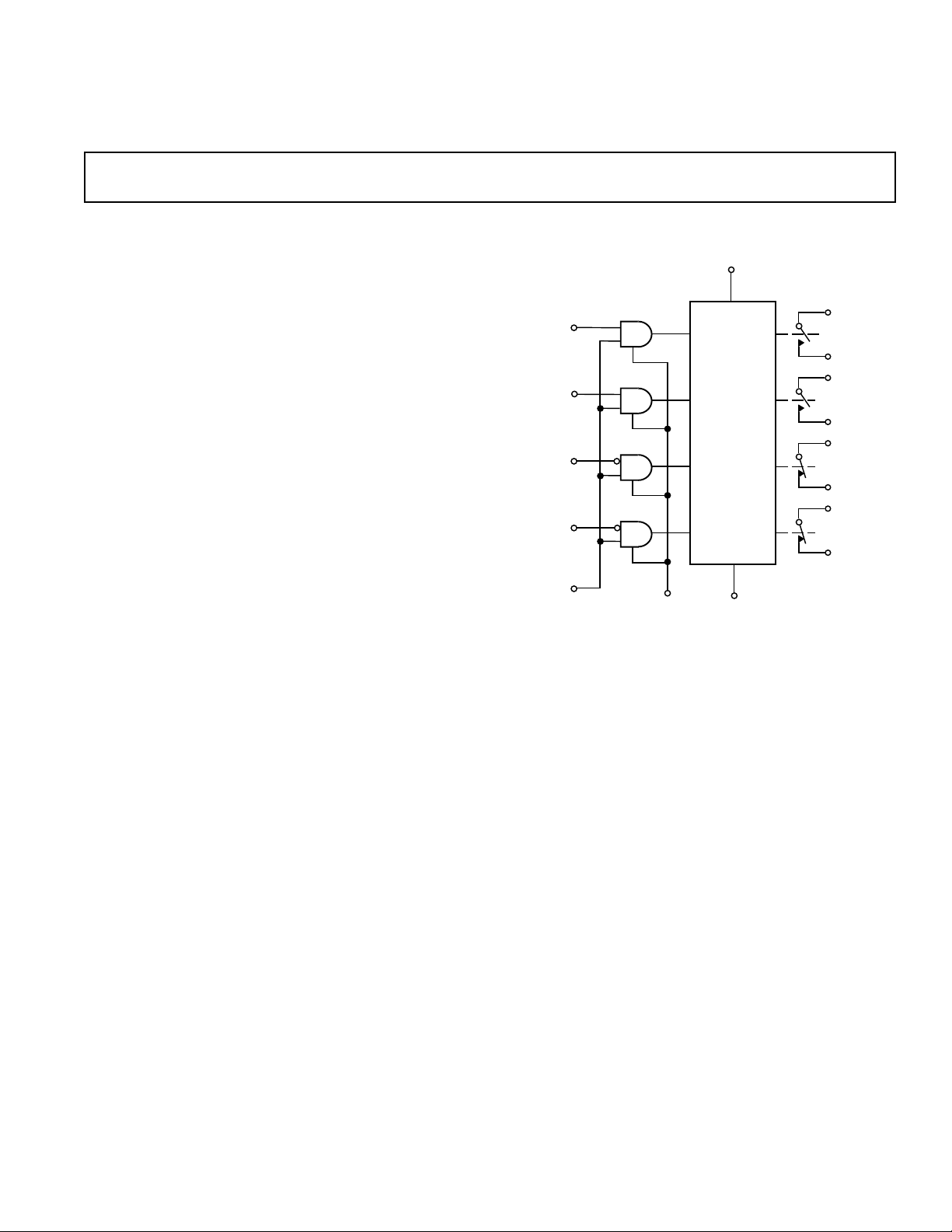
FUNCTIONAL BLOCK DIAGRAM
V+
12
1
IN 1
IN 2
IN 3
IN 4
DIS
8
9
16
13
4
GND
LEVEL
SHIFT
5
V–
SW06
3
S1
2
D1
6
S2
7
D2
11
S3
10
D3
14
S4
15
D4
GENERAL DESCRIPTION
The SW06 is a four channel single-pole, single-throw analog
switch that employs both bipolar and ion-implanted FET
devices. The SW06 FET switches use bipolar digital logic inputs
which are more resistant to static electricity than CMOS devices.
Ruggedness and reliability are inherent in the SW06 design and
construction technology.
Increased reliability is complemented by excellent electrical
specifications. Potential error sources are reduced by minimizing
“ON” resistance and controlling leakage currents at high temperatures. The switching FET exhibits minimal R
variation
ON
over a 20 V analog signal range and with power supply voltage
changes. Operation from a single positive power supply voltage
is possible. With V+ = 36 V, V– = 0 V, the analog signal range
will extend from ground to +32 V.
PNP logic inputs are TTL and CMOS compatible to allow the
SW06 to upgrade existing designs. The logic “0” and logic “1”
input currents are at microampere levels reducing loading on
CMOS and TTL logic.
REV. A
Information furnished by Analog Devices is believed to be accurate and
reliable. However, no responsibility is assumed by Analog Devices for its
use, nor for any infringements of patents or other rights of third parties
which may result from its use. No license is granted by implication or
otherwise under any patent or patent rights of Analog Devices.
One Technology Way, P.O. Box 9106, Norwood, MA 02062-9106, U.S.A.
Tel: 617/329-4700 Fax: 617/326-8703

SW06–SPECIFICA TIONS
ELECTRICAL CHARACTERISTICS
(@ V+ = +15 V, V– = –15 V and TA = +258C, unless otherwise noted)
SW06B SW06F SW06G
Parameter Symbol Conditions Min Typ Max Min Typ Max Min Typ Max Units
“ON” RESISTANCE R
ON
VS = 0 V, IS = 1 mA 60 80 60 100 100 150 Ω
VS = ±10 V, IS = 1 mA 65 80 65 100 100 150
RON MATCH BETWEEN SWITCHES RON Match VS = 0 V, IS = 100 µA
ANALOG VOLTAGE RANGE V
ANALOG CURRENT RANGE I
∆RON VS. APPLIED VOLTAGE ∆R
A
IS = 1 mA
IS = 1 mA
A
ON
VS = ±10 V 10 15 7 12 5 10 mA
–10 V ≤ VS ≤ 10 V, IS = 1.0 mA 5 15 10 20 10 20 %
2
2
SOURCE CURRENT IN
“OFF” CONDITION I
S(OFF)
VS = 10 V, VD = –10 V
DRAIN CURRENT IN
“OFF” CONDITION I
SOURCE CURRENT IN I
“ON” CONDITION I
LOGICAL “1” INPUT VOLTAGE V
LOGICAL “0” INPUT VOLTAGE V
LOGICAL “1” INPUT CURRENT I
LOGICAL “0” INPUT I
TURN-ON TIME t
D(OFF)
S(ON)+
D(ON)
INH
INL
INH
INL
ON
VS = 10 V, VD = –10 V
VS = VD = ±10 V
Full Temperature Range
Full Temperature Range
VIN = 2.0 V to 15.0 V
VIN = 0.8 V 1.5 5.0 1.5 5.0 1.5 10.0 µA
See Switching Time 340 500 340 600 340 700 ns
Test Circuit
4, 6
1
5 10 5 20 20 %
+10 +11 +10 +11 +10 +11 V
–10 –15 –10 –15 –10 –15
3
3
3
2, 4
2, 4
5
0.3 2.0 0.3 2.0 0.3 10 nA
0.3 2.0 0.3 2.0 0.3 10 nA
0.3 2.0 0.3 2.0 0.3 10 nA
2.0 2.0 2.0 V
0.8 0.8 0.8 V
55 10µA
TURN-OFF TIME t
OFF
BREAK-BEFORE-MAKE TIME tON–t
SOURCE CAPACITANCE C
DRAIN CAPACITANCE C
CHANNEL “ON” CAPACITANCE C
“OFF” ISOLATION I
CROSSTALK C
S(OFF)
D(OFF)
D(ON)+
C
S(ON)
SO(OFF)
T
POSITIVE SUPPLY CURRENT I+ All Channels “OFF”, 5.0 6.0 5.0 9.0 6.0 9.0 mA
NEGATIVE SUPPLY CURRENT I– All Channels “OFF”, 3.0 5.0 4.0 7.0 4.0 7.0 mA
GROUND CURRENT I
G
See Switching Time 200 400 200 400 200 500 ns
Test Circuit
Note 7 50 140 50 140 50 140 ns
OFF
VS = 0 V
VS = 0 V
VS = VD = 0 V
VS = 5 V rms, RL = 680 Ω,58 58 58dB
C
= 7 pF, f = 500 kHz
L
VS = 5 V rms, RL = 680 Ω,70 70 70dB
C
= 7 pF, f = 500 kHz
L
DIS = “0”
DIS = “0”
All Channels “ON” or 3.0 4.0 3.0 4.0 3.0 5.0 mA
“OFF”
4, 6
3
3
3
3
3
3
3
3
7.0 7.0 7.0 pF
5.5 5.5 5.5 pF
15 15 15 pF
–2–
REV. A

SW06
(@ V+ = +15 V, V– = –15 V, –558C ≤ TA ≤ +1258C for SW06BQ, –408C ≤ TA ≤ +858C for
ELECTRICAL CHARACTERISTICS
Parameter Symbol Conditions Min Typ Max Min Typ Max Min Typ Max Units
SW06FQ and –408C ≤ TA ≤ +858C for SW06GP/GS, unless otherwise noted)
SW06B SW06F SW06G
TEMPERATURE RANGE T
“ON” RESISTANCE R
A
ON
Operating –55 +125 –25 +85 0 70 °C
VS = 0 V, IS = 1.0 mA 75 110 75 125 75 175 Ω
VS = ±10 V, IS = 1.0 mA 80 110 80 125 80 175
∆RON MATCH BETWEEN SWITCHES RON Match VS = 0 V, IS = 100 µA
ANALOG VOLTAGE RANGE V
ANALOG CURRENT RANGE I
∆RON WITH APPLIED VOLTAGE ∆R
A
IS = 1.0 mA
IS = 1.0 mA
A
ON
VS = ±10 V 7 12 5 11 11 mA
–10 V ≤ VS ≤ 10 V, IS = 1.0 mA 10 12 15 %
2
2
SOURCE CURRENT IN VS = 10 V, VD = –10 V
“OFF” CONDITION I
S(OFF)
TA = Max Operating Temp
DRAIN CURRENT IN VS = 10 V, VD = –10 V
“OFF” CONDITION I
LEAKAGE CURRENT IN I
“ON” CONDITION I
LOGICAL “1” INPUT CURRENT I
LOGICAL “0” INPUT CURRENT I
TURN-ON TIME t
TURN-OFF TIME t
D(OFF)
S(ON)+
D(ON)
INH
INL
ON
OFF
TA = Max Operating Temp
VS = VD = ±10 V 100 30 60 nA
TA = Max Operating Temp
VIN = 2.0 V to 15.0 V
VIN = 0.8 V 4 10 4 10 5 15 µA
See Switching Time 440 900 500 900 1000 ns
Test Circuit
See Switching Time 300 500 330 500 500 ns
Test Circuit
4, 8
4, 8
1
6 20 6 25 10 %
+10 +11 +10 +11 +10 +11 V
–10 –15 –10 –15 –10 –15
3, 9
3, 9
3, 9
5
60 30 60 nA
60 30 60 nA
10 10 15 µA
BREAK-BEFORE-MAKE TIME tON–t
OFF
POSITIVE SUPPLY CURRENT I+ All Channels “OFF,” 9.0 13.5 13.5 mA
NEGATIVE SUPPLY CURRENT I– All Channels “OFF,” 7.5 10.5 10.5 mA
GROUND CURRENT I
G
NOTES
1
VS = 0 V, IS = 100 µA. Specified as a percentage of R
2
Guaranteed by RON and leakage tests. For normal operation maximum analog signal voltages should be restricted to less than (V+) –4 V.
3
Switch being tested ON or OFF as indicated, V
4
Also applies to disable pin.
5
Current tested at VIN = 2.0 V. This is worst case condition.
6
Sample tested.
7
Switch is guaranteed by design to provide break-before-make operation.
8
Guaranteed by design.
9
Parameter tested only at TA = +125°C for military grade device.
= 2.0 V or V
INH
Note 7 70 70 50 n s
DIS = “0”
DIS = “0”
All Channels “ON” or 6.0 7.5 7.5 mA
“OFF”
where: R
AVERAGE
3
3
3
R
+ R
ON1
=
AVERAGE
= 0.8 V, per logic truth table.
INL
ON2
+ R
4
ON3
+ R
ON4
.
Specifications subject to change without notice.
REV. A
–3–
SW06
W AFER TEST LIMITS
(@ V+ = +15 V, V– = –15 V, TA = +258C, unless otherwise noted)
SW06N SW06G
Parameter Symbol Conditions Limit Limit Units
“ON” RESISTANCE R
ON
–10 V ≤ VA ≤ 10 V, IS ≤ 1 mA 80 100 Ω max
RON MATCH BETWEEN SWITCHES RON Match VA = 0 V, IS ≤ 100 µA 15 20 % max
∆RON VS. V
A
∆R
ON
–10 V ≤ VA ≤ 10 V, IS ≤ 1 mA 10 20 % max
POSITIVE SUPPLY CURRENT I+ Note 1 6.0 9.0 mA max
NEGATIVE SUPPLY CURRENT I– Note 1 5.0 7.0 mA max
GROUND CURRENT I
ANALOG VOLTAGE RANGE V
LOGIC “1” INPUT VOLTAGE V
LOGIC “0” INPUT VOLTAGE V
LOGIC “0” INPUT CURRENT I
LOGIC “1” INPUT CURRENT I
ANALOG CURRENT RANGE I
NOTE
Electrical tests are performed at wafer probe to the limits shown. Due to variations in assembly methods and normal yield loss, yield after packaging is not guaranteed
for standard product dice. Consult factory to negotiate specifications based on dice lot qualification through sample lot assembly and testing.
G
A
INH
INL
INL
INH
A
Note 1 4.0 4.0 mA max
IS = 1 mA ±10.0 ±10.0 V min
Note 2 2.0 2.0 V min
Note 2 0.8 0.8 V max
0 V ≤ VIN ≤ 0.8 V 5.0 5.0 µA max
2.0 V ≤ VIN ≤ 15 V
3
55µA max
VS = ±10 mV 10 7 mA min
TYPICAL ELECTRICAL CHARACTERISTICS
(@ V+ = +15 V, V– = –15 V, TA = +258C, unless otherwise noted)
SW06N SW06G
Parameter Symbol Conditions Typical Typical Units
“ON” RESISTANCE R
TURN-ON TIME t
TURN-OFF TIME t
ON
ON
OFF
–10 V ≤ VA ≤ 10 V, IS ≤ 1 mA 60 60 Ω
340 340 ns
200 200 ns
DRAIN CURRENT IN
“OFF” CONDITION I
“OFF” ISOLATION I
CROSSTALK C
NOTES
1
Power supply and ground current specified for switch “ON” or “OFF.”
2
Guaranteed by RON and leakage tests.
3
Current tested at VIN = 2.0 V. This is worst case condition.
D(OFF)
SO(OFF)
T
VS = 10 V, VD = –10 V 0.3 0.3 nA
f = 500 kHz, RL = 680 Ω 58 58 dB
f = 500 kHz, RL = 680 Ω 70 70 dB
–4–
REV. A

SW06
ABSOLUTE MAXIMUM RATINGS
1
Operating Temperature Range
SW06BQ, BRC . . . . . . . . . . . . . . . . . . . –55°C to +125°C
SW06FQ . . . . . . . . . . . . . . . . . . . . . . . . . –40°C to +85°C
SW06GP, GS . . . . . . . . . . . . . . . . . . . . . . –40°C to +85°C
Storage Temperature Range . . . . . . . . . . . –65°C to +150°C
Lead Temperature (Soldering, 60 sec) . . . . . . . . . . . . +300°C
Maximum Junction Temperature . . . . . . . . . . . . . . . . +150°C
V+ Supply to V– Supply . . . . . . . . . . . . . . . . . . . . . . . +36 V
V+ Supply to Ground . . . . . . . . . . . . . . . . . . . . . . . . . +36 V
Logic Input Voltage . . . . . . . . . . . (–4 V or V–) to V+ Supply
Analog Input Voltage Range
Continuous . . . . . . . . . . . . . V– Supply to V+ Supply +20 V
Maximum Current Through
Any Pin Including Switch . . . . . . . . . . . . . . . . . . . . . 30 mA
Package Type u
2
JA
u
JC
Units
16-Pin Hermetic DIP (Q) 100 16 °C/W
16-Pin Plastic DIP (P) 82 39 °C/W
20-Contact LCC (RC) 98 38 °C/W
16-Pin SOL (S) 98 30 °C/W
NOTES
1
Absolute maximum ratings apply to both DICE and packaged parts, unless
otherwise noted.
2
θJA is specified for worst case mounting conditions, i.e., θJA is specified for device
in socket for Cerdip, P-DIP, and LCC packages; θJA is specified for device soldered
to printed circuit board for SO package.
ORDERING GUIDE
Temperature Package Package
Model Range Description Option
SW06BQ –55°C to +125°C Cerdip Q-16
SW06BRC –55°C to +125°C LCC E-20A
SW06FQ –40°C to +85°C Cerdip Q-16
SW06GP –40°C to +85°C Plastic DIP N-16
SW06GS –40°C to +85°C SOL R-16
TRUTH TABLE
Switch State
Disable Logic Channels Channels
Input Input 1 & 2 3 & 4
0 X OFF OFF
1 or NC 0 OFF ON
1 or NC 1 ON OFF
PIN CONNECTIONS
16-Pin DIP (Q or P-Suffix)
16-Pin SOL (S-Suffix)
DICE CHARACTERISTICS
Die Size 0.101 × 0.097 inch, 9797 sq. mils
(2.565 × 2.464 mm, 6320 sq. mm)
SW06BRC/883
LCC Package
(RC-Suffix)
REV. A
–5–

SW06–Typical Performance Characteristics
“ON” Resistance vs. Power Supply
Voltage
Switch Current vs. Voltage
“ON” Resistance vs. Analog Voltage
Leakage Current vs. Analog Voltage
RON vs. Temperature
Leakage Current vs. Temperature
Supply Current vs. Temperature
Supply Current vs. Supply Voltage
–6–
Switch Capacitance vs. Analog
Voltage
REV. A
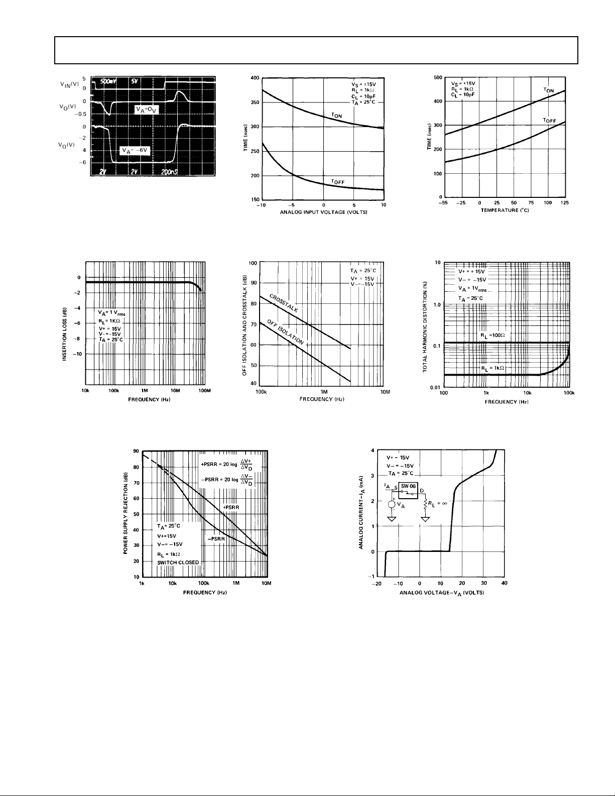
SW06
TON/T
Insertion Loss vs. Frequency
Switching Response
OFF
Switching Time vs. Analog Voltage
Crosstalk and “OFF” Isolation vs.
Frequency
Switching Time vs. Temperature
Total Harmonic Distortion
REV. A
Power Supply Rejection vs.
Frequency
Overvoltage Characteristics
–7–
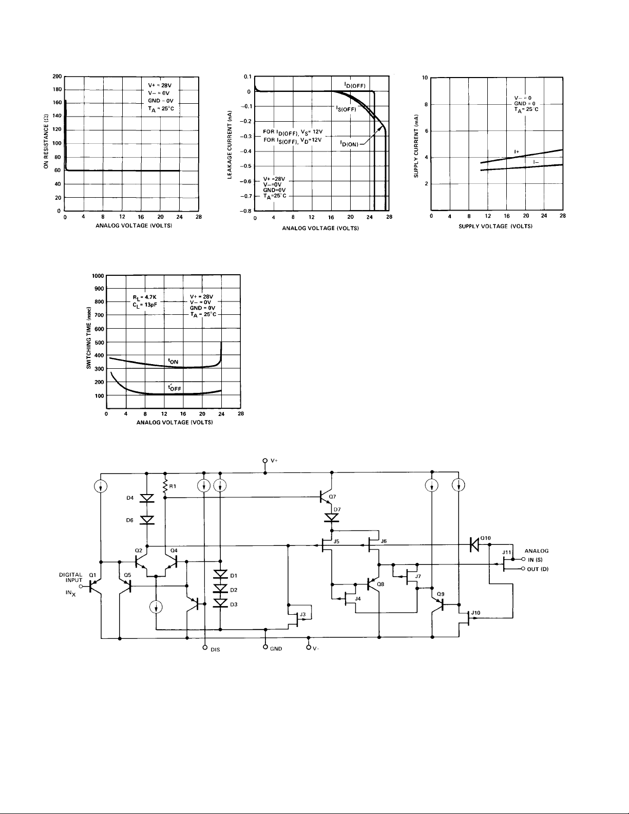
SW06–Typical Performance Characteristics (Operating and Single Supply)
“On” Resistance vs. Analog Voltage
Switching Time vs. Supply Voltage
Leakage Current vs. V
NOTE
These single-supply-operation characteristic curves are valid
when the negative power supply V– is tied to the logic ground
reference pin “GND.” TTL input compatibility is still maintained when “GND” is the same potential as the TTL ground.
t
is measured from 50% of logic input waveform to 0.9 VO.
OFF
The analog voltage range extends from 0 V to V+ –4 V; the
switch will no longer respond to logic control when V
4 volts of V+.
ANALOG
Supply Current vs. Supply Voltage
is within
A
Simplified Schematic Diagram (Typical Switch)
–8–
REV. A

“Off” Isolation Test Circuit
SW06
Crosstalk Test Circuit
Switching Time Test Circuit
REV. A
–9–

SW06
Figure 1. Functional Applications of SW06
APPLICATIONS INFORMATION
The single analog switch product configures, by appropriate pin
connections, into four switch applications. As shown in Figure
1, the SW06 connects as a QUAD SPST, a DUAL SPDT, a
DUAL DPST, or a DPDT analog switch. This versatility increases further when taking advantage of the disable input (DIS)
which turns all switches OFF when taken active low.
Ion-implantation of the JFET analog switch achieves low ON
resistance and tight channel-to-channel matching. Combining
the low ON resistance and low leakage currents results in a
worst case voltage error figure V
R
= 100 nA × 100 Ω = 11 microvolts. This amount of er-
SD(ON)
@ +125°C = I
ERROR
D(ON)
×
ror is negligible considering dissimilar-metal thermally-induced
offsets will be in the 5 to 15 microvolt range.
LOGIC INPUTS
The logic inputs (INX) and disable input (DIS) are referenced
to a TTL logic threshold value of two forward diode drops (1.4 V
at +25°C) above the GND terminal. These inputs use PNP
transistors which draw maximum current at a logic “0” level and
drops to a leakage current of a reverse biased diode as the logic
input voltage raises above 1.4 volts. Any logic input voltage
greater than 2.0 volts becomes logic “1,” less than 0.8 volts becomes logic “0” resulting in full TTL noise immunity not available from similar CMOS input analog switches. The PNP
transistor inputs require such low input current that the SW06
approaches fan-ins of CMOS input devices. These bipolar logic
inputs exceed any CMOS input circuit in resistance to static
voltage and radiation susceptibility. No damage will occur to the
SW06 if logic high voltages are present when the SW06 power
supplies are OFF. When the V+ and V– supplies are OFF, the
logic inputs present a reverse bias diode loading to active logic
inputs. Input logic thresholds are independent of V+ and V–
supplies making single V+ supply operation possible by simply
connecting GND and V– together to the logic ground supply.
ANALOG VOLTAGE AND CURRENT
ANALOG VOLTAGE
These switches have constant ON resistance for analog voltages
from the negative power supply (V–) to within 4 volts of the
positive power supply. This characteristic shown in the plots results in good total harmonic distortion, especially when compared to CMOS analog switches that have a 20 to 30 percent
variation in ON resistance versus analog voltage. Positive analog
input voltage should be restricted to 4 volts less than V+ assuring the switch remains open circuit in the OFF state. No increase in switch ON resistance occurs when operating at supply
voltages less than ±15 volts (see plot). Small signals have a 3 dB
down frequency of 70 MHz (see insertion loss versus frequency
plot).
ANALOG CURRENT
The analog switches in the ON state are JFETs biased in their
triode region and act as switches for analog current up to the I
A
specification (see plot of IDS vs VDS). Some applications require
pulsed currents exceeding the I
spec. For example, an integra-
A
tor reset switch discharging a shunt capacitor will produce a
peak current of I
A(PEAK)
= V
CAP/RDS(ON)
. In this application, it is
best to connect the source to the most positive end of the capacitor, thereby achieving the lowest switch resistance and
–10–
REV. A

SW06
fastest reset times. The switch can easily handle any amount of
capacitor discharge current subject only to the maximum heat
dissipation of the package and the maximum operating junction
temperature from which repetition can be established.
SWITCHING
Switching time tON and t
V
than t
and temperature. In all cases, t
ANALOG
to ensure a break-before-make interval for SPDT and
ON
characteristics are plotted versus
OFF
is designed faster
OFF
DPDT applications. The disable input (DIS) has the same
switching times (t
ON
and t
) as the logic inputs (INX).
OFF
Switching transients occurring at the source and drain contacts
results from ac coupling of the switching FETs gate-to-source
and gate-to-drain coupling capacitance. The switch turn ON
will cause a negative going spike to occur and the turn OFF will
cause a positive spike to occur. These spikes can be reduced by
additional capacitance loading, lower values of R
, or switching
L
an additional switch (with its extra contact floating) to the opposite state connected to the spike sensitive node.
Typical Applications
DISABLE NODE
This TTL compatible node is similar to the logic inputs INX but
has an internal 2 µA current source pull-up. If disable is left un-
connected, it will assume the logic “1” state, then the state of
the switches is controlled only by the logic inputs IN
POWER SUPPLIES
.
X
This product operates with power supply voltages ranging from
±12 to ±18 volts; however, the specifications only guarantee
device parameters with ±15 volt ±5% power supplies. The
power supply sensitive parameters have plots to indicate effects
of supply voltages other than ± 15 volts.
Operation from Single Positive Power Supply
High Off Isolation Selector Switch (Shunt-Series Switch)
REV. A
4-Channel Sample Hold Amplifier
–11–

SW06
Single Pole Double Throw Selector Switch with Break-Before-Make Interval
OUTLINE DIMENSIONS
Dimensions shown in inches and (mm).
0.358 (9.09)
0.342 (8.69)
SQ
0.210 (5.33)
MAX
0.160 (4.06)
0.115 (2.93)
20-Terminal Leadless Chip Carrier
(RC-Suffix)
E-20A
0.200 (5.08)
BSC
REF
0.055 (1.40)
0.045 (1.14)
0.075
(1.91)
REF
19
18
14
13
20
1
BOTTOM
VIEW
0.150 (3.81)
BSC
0.100 (2.54)
0.064 (1.63)
0.358
(9.09)
MAX
SQ
0.088 (2.24)
0.054 (1.37)
0.095 (2.41)
0.075 (1.90)
0.011 (0.28)
0.007 (0.18)
R TYP
0.075 (1.91)
16-Lead Plastic DIP
(P-Suffix)
N-16
0.840 (21.33)
0.745 (18.93)
16
18
PIN 1
0.022 (0.558)
0.014 (0.356)
0.100
(2.54)
BSC
9
0.280 (7.11)
0.240 (6.10)
0.060 (1.52)
0.015 (0.38)
0.130
(3.30)
MIN
0.070 (1.77)
0.045 (1.15)
SEATING
PLANE
0.100 (2.54) BSC
0.015 (0.38)
3
MIN
4
0.028 (0.71)
0.022 (0.56)
0.050 (1.27)
8
BSC
9
45° TYP
0.325 (8.25)
0.300 (7.62)
0.015 (0.381)
0.008 (0.204)
0.195 (4.95)
0.115 (2.93)
0.005 (0.13) MIN
PIN 1
0.200
(5.08)
MAX
0.200 (5.08)
0.125 (3.18)
0.0118 (0.30)
0.0040 (0.10)
16
1
0.023 (0.58)
0.014 (0.36)
16 9
PIN 1
0.0500
(1.27)
BSC
16-Lead Cerdip
(Q-Suffix)
Q-16
0.080 (2.03) MAX
9
0.310 (7.87)
0.220 (5.59)
8
0.840 (21.34) MAX
0.100
(2.54)
BSC
0.070 (1.78)
0.030 (0.76)
0.060 (1.52)
0.015 (0.38)
SEATING
PLANE
16-Lead Wide Body SOL
(S-Suffix)
R-16/SOL-16
0.4133 (10.50)
0.3977 (10.00)
0.2992 (7.60)
0.2914 (7.40)
0.4193 (10.65)
0.0192 (0.49)
0.0138 (0.35)
81
0.1043 (2.65)
0.0926 (2.35)
SEATING
PLANE
0.3937 (10.00)
0.0125 (0.32)
0.0091 (0.23)
0.150
(3.81)
MIN
0.320 (8.13)
0.290 (7.37)
15°
0.0291 (0.74)
0.0098 (0.25)
0.0500 (1.27)
8°
0°
0.0157 (0.40)
0.015 (0.38)
0.008 (0.20)
0°
x 45°
–12–
REV. A
 Loading...