High End, Multichannel,
a
32-Bit Floating-Point Audio Processor
FEATURES
Super Harvard Architecture Computer (SHARC)
4 Independent Buses for Dual Data, Instruction, and
I/O Fetch on a Single Cycle
32-Bit Fixed-Point Arithmetic; 32-Bit and 40-Bit Floating
Point Arithmetic
544 Kbits On-Chip SRAM Memory, Integrated I/O
Peripheral I
Transmit
2
S Support for
Channels
8 Simultaneous Receive and
66 MIPS, 198 MFLOPS Peak, 132 MFLOPS Sustained
Performance
User-Configurable 544 Kbits On-Chip SRAM Memory
2 External Port, DMA Channels and 8 Serial Port,
DMA Channels
Decodes Industry Standard Formats Using a 32-Bit
Floating Point Implementation for Decoding
®
Digital AC-3, Dolby Digital EX Processing
Dolby
Dolby Pro Logic
®
, 96 kHz, Dolby Pro Logic II
Dolby Headphone, Dolby 3/0
DTS® 5.1, DTS-ES®-Discreet 6.1, DTS Matrix and Matrix 3.0,
DTS 96/24®, DTS NEO:6
®
THX
Ultra, Select, Ultra2, 5.1, 7.1, EX
®
Labs Circle Surround IITM, Virtual Loudspeaker
SRS
MPEG AAC, MPEG2 Decode, MPEG 2-Channel Decode
PCM, PCM 96 kHz
HDCD, MLP*
Delay 7.1, 96 kHz
Bass 7.1, 96 kHz, Bass/Treble 2 Channel
ADI Surround: Club, Music, and Stadium
AAC (LC), AAC (LC) 2 Channel, AAC MP
WaveSurround 5.1 Channel to Headphone, Stereo to
Headphone, Channel to Loudspeaker, Stereo to
Loudspeaker
Downsampling 96 kHz to 48 kHz (2-Channel)
3-Band Equalizer, 2-Channel
Encoders: AC-3 2-Channel Consumer Encoder
Single Chip DSP-Based Implementation of Digital Audio
Algorithms
2
S Compatible Ports
I
Interface to External SDRAM
®
SST-Melody®-SHARC
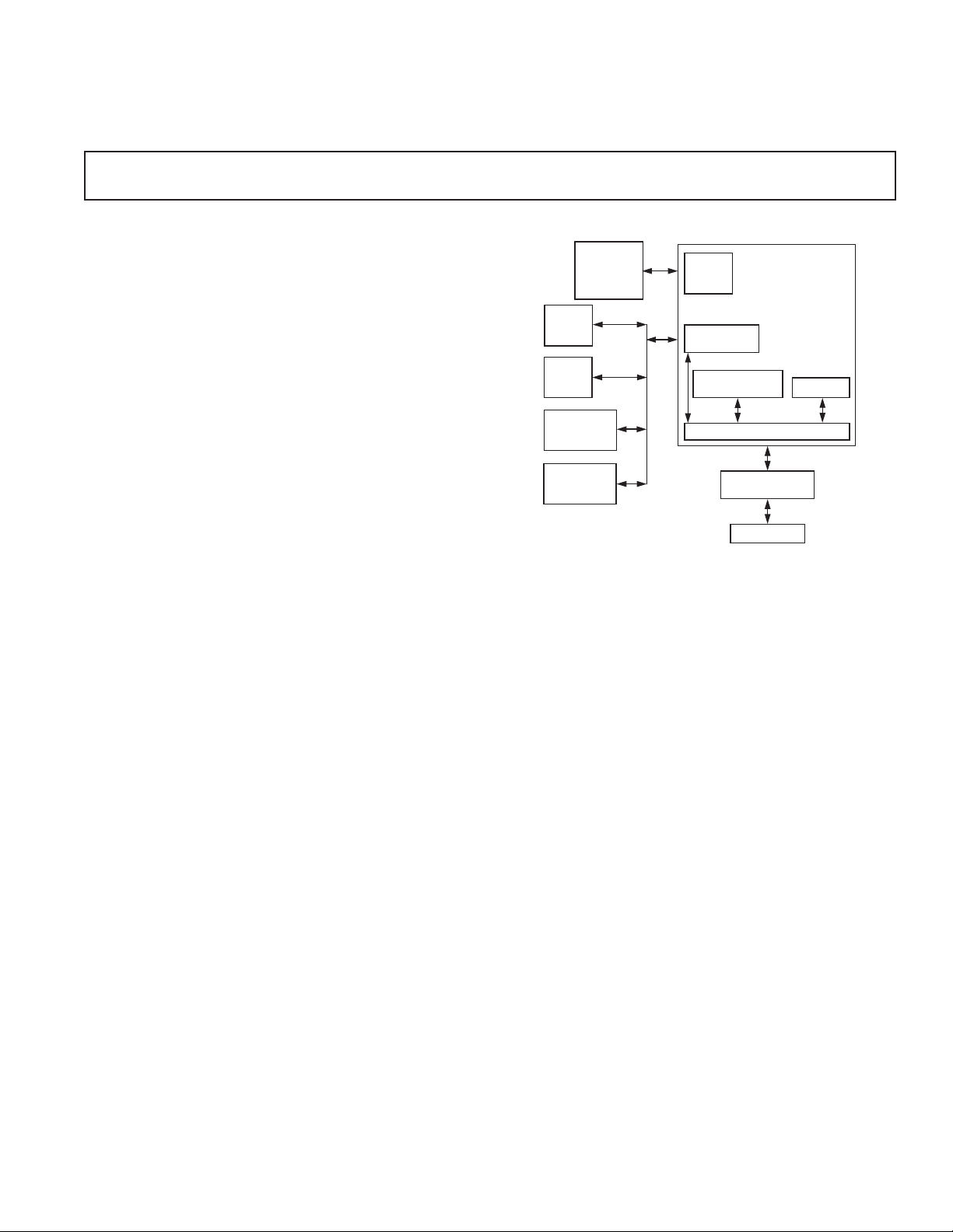
FUNCTIONAL BLOCK DIAGRAM
SDRAM
128K ⴛ 32,
BOOT ROM
-
1M ⴛ 8
ADC
DAC
S/PDIF
TRANSMITTER
S/PDIF
RECEIVER
Easy Interfaces to Audio Codecs
96 kHz Processing
Supports Customer Specific Post Processing
Automatic Stream Detection and Code Loading
Easy to Use Software Architecture
Optimized Library of Routines
Host Communication Using 16-Bit Parallel Port or SPI Port
Highly Flexible Serial Ports
SRAM Interface for More Delay
Supports IEC60958 For Bit Streams
8-Channel Output Using TDM Codecs
APPLICATIONS
Home Theater AVR Systems
Automotive Audio Receivers
Video Game Consoles
DVD Players
Cable and Satellite Set-Top Boxes
Multimedia Audio/Video Gateways
IRQ
GPIO
SST-Melody-SHARC
SERIAL PORT
ALGORITHMS
KERNEL
DMA CONNECTION
OR DUAL BUFFER
HOST MICRO
COMMAND
Melody and SHARC are registered trademarks of Analog Devices, Inc.
DTS, DTS-ES, and DTS 96/24 are registered trademarks of Digital Theater
Systems, Inc.
Dolby and Pro Logic are registered trademarks of Dolby Laboratories
Licensing Corporation.
SRS is a registered trademark and Circle Surround II is a trademark of SRS Labs.
THX is a registered trademark of the THX, Ltd.
*MLP is implemented, not certified.
REV. 0
Information furnished by Analog Devices is believed to be accurate and
reliable. However, no responsibility is assumed by Analog Devices for its
use, nor for any infringements of patents or other rights of third parties that
may result from its use. No license is granted by implication or otherwise
under any patent or patent rights of Analog Devices.
GENERAL DESCRIPTION
The SST-Melody-SHARC family of powerful 32-bit Audio Processors
from Analog Devices provides flexible solutions and delivers
a host of features across high end and high fidelity audio systems
to the AV receiver and DVD markets. It includes multichannel
audio decoders, encoders, and post processors for digital
audio designs using DSP chipsets in home theater systems and
automotive audio receivers.
(continued on page 11)
One Technology Way, P.O. Box 9106, Norwood, MA 02062-9106, U.S.A.
Tel: 781/329-4700 www.analog.com
Fax: 781/326-8703 © Analog Devices, Inc., 2002

SST-Melody-SHARC–SPECIFICATIONS
RECOMMENDED OPERATING CONDITIONS
1
Test C Grade K Grade
Parameter Conditions Min Max Min Max Unit
V
DD
T
CASE
V
IH
V
IL1
V
IL2
NOTES
1
See Environmental Conditions section for information on thermal specifications.
2
Applies to input and bidirectional pins: DATA31–0, ADDR23–0, BSEL, RD, WR, SW, ACK, SBTS, IRQ2–0, FLAG11–0, HBG, CS, DMAR1, DMAR2, BR2–1, ID2–0,
RPBA, CPA, TFS0, TFS1, RFS0, RFS1, BMS, TMS, TDI, TCK, HBR, DR0A, DR1A, DR0B, DR1B, TCLK0, TCLK1, RCLK0, RCLK1, RESET, TRST,
PWM_EVENT0, PWM_EVENT1, RAS, CAS , SDWE, SDCKE.
3
Applies to input pin CLKIN.
Supply Voltage 3.13 3.60 3.13 3.60 V
Case Operating Temperature –40 +100 0 +85 °C
High Level Input Voltage @ VDD = max 2.0 VDD + 0.5 2.0 VDD + 0.5 V
Low Level Input Voltage2@ VDD = min –0.5 +0.8 –0.5 +0.8 V
Low Level Input Voltage3@ VDD = min –0.5 +0.7 –0.5 +0.7 V
ELECTRICAL CHARACTERISTICS
C and K Grades
Parameter Test Conditions Min Max Unit
3
4
1
3
1
5, 6, 7, 8
5
6
9
8
7
@ VDD = min, IOH = –2.0 mA
@ VDD = min, IOL = +4.0 mA
@ VDD = max, VIN = VDD max 10 µA
@ VDD = max, VIN = 0 V 10 µA
@ VDD = max, VIN = 0 V 150 µA
@ VDD = max, VIN = VDD max 10 µA
@ VDD = max, VIN = 0 V 8 µA
@ VDD = max, VIN = 0 V 150 µA
@ VDD = max, VIN = 1.5 V 350 µA
@ VDD = max, VIN = 0 V 4 mA
@ VDD = max, VIN = 0 V 1.5 mA
fIN = 1 MHz, T
= 25°C, VIN = 2.5 V 8 pF
CASE
V
OH
V
OL
I
IH
I
IL
I
ILP
I
OZH
I
OZL
I
OZLS
I
OZLA
I
OZLAR
I
OZLC
C
IN
NOTES
1
Applies to output and bidirectional pins: DATA31–0, ADDR 23–0, MS3–0, RD, WR, SW, ACK, FLAG11–0, HBG, REDY, DMAG1, DMAG2, BR2–1, CPA,
TCLK0, TCLK1, RCLK0, RCLK1, TFS0, TFS1, RFS0, RFS1, DT0A, DT1A, DT0B, DT1B, XTAL, BMS, TDO, EMU, BMSTR, PWM_EVENT0,
PWM_EVENT1, RAS, CAS, DQM, SDWE, SDCLK0, SDCLK1, SDCKE, SDA10.
2
See Output Drive Current section for typical drive current capabilities.
3
Applies to input pins: ACK, SBTS, IRQ2–0, HBR, CS, DMAR1, DMAR2, ID1–0, BSEL, CLKIN, RESET , TCK (Note that ACK is pulled up internally with 2 k Ω
during reset in a multiprocessor system, when ID1–0 = 01 and another SST-Melody-SHARC is not requesting bus mastership).
4
Applies to input pins with internal pull-ups: DR0A, DR1A, DR0B, DR1B, TRST, TMS, TDI.
5
Applies to three-statable pins: DATA31–0, ADDR 23–0, MS3–0, RD, WR, SW, ACK, FLAG11–0, REDY, HBG, DMAG1, DMAG2, BMS, TDO, RAS, CAS,
DQM, SDWE, SDCLK0, SDCLK1, SDCKE, SDA10, and EMU (note that ACK is pulled up internally with 2 kΩ during reset in a multiprocessor system,
when ID1–0 = 01 and another SST-Melody-SHARC is not requesting bus mastership).
6
Applies to three-statable pins with internal pull-ups: DT0A, DT1A, DT0B, DT1B, TCLK0, TCLK1, RCLK0, RCLK1.
7
Applies to CPA pin.
8
Applies to ACK pin when pulled up.
9
Applies to ACK pin when keeper latch enabled.
10
Guaranteed but not tested.
11
Applies to all signal pins.
Specifications subject to change without notice.
High Level Output Voltage
Low Level Output Voltage
High Level Input Current
Low Level Input Current
Low Level Input Current
Three-State Leakage Current
Three-State Leakage Current
Three-State Leakage Current
Three-State Leakage Current
Three-State Leakage Current
Three-State Leakage Current
Input Capacitance
10, 11
2
2
2.4 V
0.4 V
REV. 0–2–

SST-Melody-SHARC
ABSOLUTE MAXIMUM RATINGS*
Supply Voltage . . . . . . . . . . . . . . . . . . . . . . . . –0.3 V to +4.6 V
Input Voltage . . . . . . . . . . . . . . . . . . . . . –0.5 V to V
Output Voltage Swing . . . . . . . . . . . . . . –0.5 V to V
Load Capacitance . . . . . . . . . . . . . . . . . . . . . . . . . . . . 200 pF
Junction Temperature Under Bias . . . . . . . . . . . . . . . . . 130°C
Storage Temperature Range . . . . . . . . . . . . . –65°C to +150°C
Lead Temperature (5 seconds) . . . . . . . . . . . . . . . . . . . . 280°C
*Stresses greater than those listed under Absolute Maximum Ratings may cause
permanent damage to the device. These are stress ratings only; functional operation of the device at these or any other conditions greater than those indicated in
the operational sections of this specification is not implied. Exposure to absolute
maximum rating conditions for extended periods may affect device reliability.
Case Temperature Instruction On-Chip Operating Package
Part Number Range Rate (MHz) SRAM (Kbit) Voltage (V) Options
ADSST-21065LKS-240 0°C to 85°C60 544 3.3 S-208-2
ADSST-21065LCS-240 –40°C to +100°C60 544 3.3 S-208-2
ADSST-21065LKCA-240 0°C to 85°C60 544 3.3 BC-196
ADSST-21065LKS-264 0°C to 85°C66 544 3.3 S-208-2
ADSST-21065LKCA-264 0°C to 85°C66 544 3.3 BC-196
+ 0.5 V
DD
+ 0.5 V
DD
ORDERING GUIDE
CAUTION
ESD (electrostatic discharge) sensitive device. Electrostatic charges as high as 4000 V readily
accumulate on the human body and test equipment and can discharge without detection. Although the
SST-Melody-SHARC features proprietary ESD protection circuitry, permanent damage may occur
on devices subjected to high energy electrostatic discharges. Therefore, proper ESD precautions are
recommended to avoid performance degradation or loss of functionality.
REV. 0
–3–

SST-Melody-SHARC
208-LEAD MQFP PIN CONFIGURATIONS
PWM
PWM
VDD
RSF0
GND
RCLK0
DR0A
DR0B
TFS0
TCLK0
VDD
GND
DT0A
DT0B
RFS1
GND
RCLK1
DR1A
DR1B
TFS1
TCLK1
VDD
VDD
DT1A
DT1B
EVENT1
GND
EVENT0
BR1
BR2
VDD
CLKIN
XTAL
VDD
GND
SDCLK1
GND
VDD
SDCLK0
DMAR1
DMAR2
HBR
GND
RAS
CAS
SDWE
VDD
DQM
SDCKE
SDA10
GND
DMAG1
DMAG2
HBG
NC
IRQ2
IRQ1
208
207
206
1
2
PIN 1
IDENTIFIER
3
4
5
6
7
8
9
10
11
12
13
14
15
16
17
18
19
20
21
22
23
24
25
26
27
28
29
30
31
32
33
34
35
36
37
38
39
40
41
42
43
44
45
46
47
48
49
50
51
52
535455565758596061
CS
VDD
BMSTR
IRQ0
205
SBTS
GND
204
GND
VDD
NCNCFLAG3
203
202
201
200
RD
WR
VDD
GND
FLAG2
FLAG1
FLAG0
ADDR0
ADDR1
GND
199
198
197
196
195
194
62636465666768
SW
CPA
VDD
GND
REDY
VDD
VDD
ADDR2
193
192
69
ACK
GND
VDD
ADDR3
ADDR4
ADDR5
191
188
190
189
ADSST-21065L
73747576777879
71
72
70
MS0
MS1
GND
GND
GND
186
185
184
ADDR8
183
182
GND
187
VDD
ADDR6
ADDR7
OO
TOP VIEW
(Not to Scale)
MS2
MS3
VDD
FLAG9
FLAG11
FLAG10
NC = NO CONNECT
ADDR10
ADDR11
GND
178
177
179
DATA0
DATA1
DATA2
VDD
176
VDD
ADDR12
ADDR13
ADDR14
175
174
173
DATA3
DATA4
DATA5
ADDR9
GND
181
180
80
8182838486878889908591
GND
FLAG8
VDD
ADDR15
ADDR16
ADDR17
172
171
170
169
92939496979899
GND
DATA6
DATA7
DATA8
GND
168
VDD
ADDR18
GND
167
166
95
VDD
GND
VDD
ADDR19
ADDR20
165
164
163
DATA9
DATA10
ADDR21
ADDR22
162
161
100
GND
DATA11
ADDR23
GND
160
159
101
102
DATA12
DATA13
NC
VDD
158
103
NC
RESET
157
156
155
154
153
152
151
150
149
148
147
146
145
144
143
142
141
140
139
138
137
136
135
134
133
132
131
130
129
128
127
126
125
124
123
122
121
120
119
118
117
116
115
114
113
112
111
110
109
108
107
106
105
104
DATA14
VDD
GND
GND
BMS
BSEL
TCK
GND
TMS
TDI
TRST
TDO
EMU
ID0
ID1
NC
VDD
VDD
GND
FLAG4
FLAG5
FLAG6
GND
FLAG7
DATA31
DATA30
VDD
VDD
GND
DATA29
DATA28
DATA27
GND
VDD
DATA26
DATA25
DATA24
VDD
GND
DATA23
DATA22
DATA21
NC
GND
DATA20
DATA19
DATA18
VDD
DATA17
DATA16
DATA15
GND
VDD
REV. 0–4–

SST-Melody-SHARC
196-BALL CSPBGA PIN CONFIGURATION
14 13 12 11 10 9 8 7 6 5 4 3 2 1
NC7
TCK
TDO
EMU
FLAG4
FLAG7
DATA29
DATA26
DATA23
DATA22
DATA18
DATA15
NC8
GND
BSEL
TRST
ID1
FLAG5
DATA30
DATA27
DATA25
DATA20
DATA17
DATA14
ADDR18
ADDR23
RESET
TMS
TDI
FLAG6
DATA31
DATA28
DATA24
DATA21
DATA16
DATA12
ADDR17
ADDR21
ADDR22
BMS
ID0
VDD
VDD
VDD
VDD
DATA19
DATA13
DATA9
ADDR14
ADDR19
ADDR20
VDD
VDD
GND
GND
GND
GND
VDD
DATA8
DATA5
ADDR11
ADDR15
ADDR16
VDD
GND
GND
GND
GND
GND
GND
VDD
DATA2
ADDR8
ADDR12
ADDR13
VDD
GND
GND
GND
GND
GND
GND
VDD
FLAG10
ADDR7
ADDR9
ADDR10
VDD
GND
GND
GND
GND
GND
GND
VDD
ACK
ADDR6
ADDR5
ADDR4
VDD
GND
GND
GND
GND
GND
GND
VDD
CPA
ADDR3
ADDR2
ADDR1
FLAG1
VDD
GND
GND
GND
GND
VDD
VDD
RD
ADDR0
FLAG0
FLAG3
IRQ1
RFS1
VDD
VDD
VDD
VDD
SDWE
DMAG2
CS
FLAG2
IRQ0
IRQ2
DR0B
DT0A
DR1A
DT1A
BR2
SDCLK1
HBR
SDA10
DMAG1
NC2
RFS0
RCLK0
TFS0
DT0B
DR1B
DT1B
BR1
XTAL
SDCLK0
CAS
SDCKE
NC1
DR0A
TCLK0
RCLK1
TFS1
TCLK1
PWM_
EVENT1
PWM_
EVENT0
CLKIN
DMAR1
DMAR2
RAS
A
B
C
D
E
F
G
H
J
K
L
M
NC6
NC5
DATA11
DATA6
DATA10
DATA3
DATA7
DATA0
DATA4
FLAG8
DATA1
FLAG9
FLAG11
MS3
MS1
MS2
GND
MS0
REDY
SW
SBTS
WR
BMSTR
GND
HBG
NC4
DQM
NC3
N
P
REV. 0
–5–

SST-Melody-SHARC
208-LEAD MQFP PIN CONFIGURATION
Pin No. Mnemonic Pin No. Mnemonic Pin No. Mnemonic Pin No. Mnemonic
1 V
DD
2 RFS0
3GND
4 RCLK0
5 DR0A
6 DR0B
7 TFS0
8 TCLK0
9V
DD
10 GND
11 DT0A
12 DT0B
13 RFS1
14 GND
15 RCLK1
16 DR1A
17 DR1B
18 TFS1
19 TCLK1
20 V
21 V
DD
DD
22 DT1A
23 DT1B
24 PWM_EVENT1
25 GND
26 PWM_EVENT0
27 BR1
28 BR2
29 V
DD
30 CLKIN
31 XTAL
32 V
DD
33 GND
34 SDCLK1
35 GND
36 V
DD
37 SDCLK0
38 DMAR1
39 DMAR2
40 HBR
41 GND
42 RAS
43 CAS
44 SDWE
45 V
DD
46 DQM
47 SDCKE
48 SDA10
49 GND
50 DMAG1
51 DMAG2
52 HBG
53 BMSTR
54 V
DD
55 CS
56 SBTS
57 GND
58 WR
59 RD
60 GND
61 V
DD
62 GND
63 REDY
64 SW
65 CPA
66 V
67 V
DD
DD
68 GND
69 ACK
70 MS0
71 MS1
72 GND
73 GND
74 MS2
75 MS3
76 FLAG11
77 V
DD
78 FLAG10
79 FLAG9
80 FLAG8
81 GND
82 DATA0
83 DATA1
84 DATA2
85 V
DD
86 DATA3
87 DATA4
88 DATA5
89 GND
90 DATA6
91 DATA7
92 DATA8
93 V
DD
94 GND
95 V
DD
96 DATA9
97 DATA10
98 DATA11
99 GND
100 DATA12
101 DATA13
102 NC
103 NC
104 DATA14
105 V
DD
106 GND
107 DATA15
108 DATA16
109 DATA17
110 V
DD
111 DATA18
112 DATA19
113 DATA20
114 GND
115 NC
116 DATA21
117 DATA22
118 DATA23
119 GND
120 V
DD
121 DATA24
122 DATA25
123 DATA26
124 V
DD
125 GND
126 DATA27
127 DATA28
128 DATA29
129 GND
130 V
131 V
DD
DD
132 DATA30
133 DATA31
134 FLAG7
135 GND
136 FLAG6
137 FLAG5
138 FLAG4
139 GND
140 V
141 V
DD
DD
142 NC
143 ID1
144 ID0
145 EMU
146 TDO
147 TRST
148 TDI
149 TMS
150 GND
151 TCK
152 BSEL
153 BMS
154 GND
155 GND
156 V
DD
157 RESET
158 V
DD
159 GND
160 ADDR23
161 ADDR22
162 ADDR21
163 V
DD
164 ADDR20
165 ADDR19
166 ADDR18
167 GND
168 GND
169 ADDR17
170 ADDR16
171 ADDR15
172 V
DD
173 ADDR14
174 ADDR13
175 ADDR12
176 V
DD
177 GND
178 ADDR11
179 ADDR10
180 ADDR9
181 GND
182 V
DD
183 ADDR8
184 ADDR7
185 ADDR6
186 GND
187 GND
188 ADDR5
189 ADDR4
190 ADDR3
191 V
192 V
DD
DD
193 ADDR2
194 ADDR1
195 ADDR0
196 GND
197 FLAG0
198 FLAG1
199 FLAG2
200 V
DD
201 FLAG3
202 NC
203 NC
204 GND
205 IRQ0
206 IRQ1
207 IRQ2
208 NC
REV. 0–6–
 Loading...