Low Power Audio Codec
FEATURES
Stereo, 24-bit analog-to-digital and digital-to-analog converters
DAC SNR: 100 dB (A-weighted), THD: −80 dB at 48 kHz, 3.3 V
ADC SNR: 90 dB (A-weighted), THD: −80 dB at 48 kHz, 3.3 V
Stereo line inputs
Low power
7 mW stereo playback (1.8 V/1.5 V supplies)
14 mW record and playback (1.8 V/1.5 V supplies)
Low supply voltages
Analog: 1.8 V to 3.6 V
Digital: 1.5 V to 3.6 V
256/384 oversampling rate in normal mode;
250/272 oversampling rate in USB mode
Audio sampling rates: 8 kHz, 11.025 kHz, 12 kHz, 16 kHz,
22.05 kHz, 24 kHz, 32 kHz, 44.1 kHz, 48 kHz, 88.2 kHz,
and 96 kHz
20-lead, 4 mm × 4 mm LFCSP (QFN) package
APPLICATIONS
Mobile phones
MP3 players
Portable gaming
Portable electronics
Educational toys
SSM2604
GENERAL DESCRIPTION
The SSM2604 is a low power, high quality stereo audio codec
for portable digital audio applications with one set of stereo
programmable gain amplifier (PGA) line inputs. It features two
24-bit analog-to-digital converter (ADC) channels and two
24-bit digital-to-analog (DAC) converter channels.
The SSM2604 can operate as a master or a slave. It supports
various master clock frequencies, including 12 MHz or 24 MHz
for USB devices; standard 256 f
12.288 MHz and 24.576 MHz; and many common audio sampling rates, such as 96 kHz, 88.2 kHz, 48 kHz, 44.1 kHz, 32 kHz,
24 kHz, 22.05 kHz, 16 kHz, 12 kHz, 11.025 kHz, and 8 kHz.
The SSM2604 can operate at power supplies as low as 1.8 V for
the analog circuitry and as low as 1.5 V for the digital circuitry.
The maximum voltage supply is 3.6 V for all supplies.
The SSM2604 is specified over the industrial temperature range
of −40°C to +85°C. It is available in a 20-lead, 4 mm × 4 mm
lead frame chip scale package (LFCSP).
or 384 fS based rates, such as
S
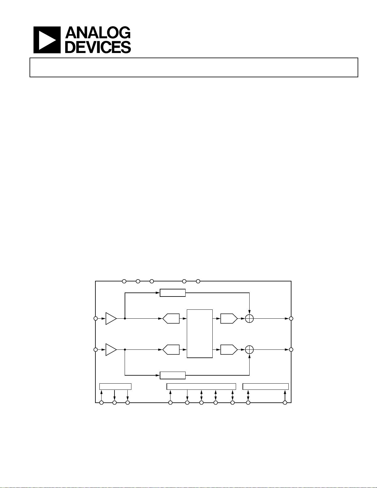
FUNCTIONAL BLOCK DIAGRAM
AVDDVMID AGND DVDD DGND
BYPASS
–34.5dB TO +33dB,
1.5dB STEP
RLINEIN
LLINEIN
–34.5dB TO +33dB,
1.5dB STEP
CLK
MCLK/
XTO CLKOUT
XTI
Rev. 0
Information furnished by Analog Devices is believed to be accurate and reliable. However, no
responsibility is assumed by Analog Devices for its use, nor for any infringements of patents or other
rights of third parties that may result from its use. Specifications subject to change without notice. No
license is granted by implication or otherwise under any patent or patent rights of Analog Devices.
Trademarks and registered trademarks are the property of their respective owners.
ADC
ADC
BYPASS
DIGITAL AUDIO INTERFACE
PBDAT RECDAT BCLK PBLRC RECLRC
SSM2604
DAC
DIGITAL
PROCESSOR
DAC
CONTROL I NTERFACE
SDIN SCLK
Figure 1.
One Technology Way, P.O. Box 9106, Norwood, MA 02062-9106, U.S.A.
Tel: 781.329.4700 www.analog.com
Fax: 781.461.3113 ©2008 Analog Devices, Inc. All rights reserved.
ROUT
LOUT
06978-001

SSM2604
TABLE OF CONTENTS
Features .............................................................................................. 1
Applications ....................................................................................... 1
General Description ......................................................................... 1
Functional Block Diagram .............................................................. 1
Revision History ............................................................................... 2
Specifications ..................................................................................... 3
Digital Filter Characteristics ....................................................... 4
Timing Characteristics ................................................................ 5
Absolute Maximum Ratings ............................................................ 7
Thermal Resistance ...................................................................... 7
ESD Caution .................................................................................. 7
Pin Configuration and Function Descriptions ............................. 8
Typical Performance Characteristics ............................................. 9
Converter Filter Response ........................................................... 9
Digital De-Emphasis .................................................................. 10
Theory of Operation ...................................................................... 11
Digital Core ................................................................................. 11
ADC and DAC ............................................................................ 11
ADC High-Pass and DAC De-Emphasis Filters .................... 11
Analog Interface ......................................................................... 12
Digital Audio Interface .............................................................. 12
Software Control Interface ........................................................ 15
Typical Application Circuits ......................................................... 16
Register Map ................................................................................... 17
Register Map Details ...................................................................... 18
Left-Channel ADC Input Volume, Address 0x00 .................. 18
Right-Channel ADC Input Volume, Address 0x01 ............... 19
Analog Audio Path, Address 0x04 ........................................... 20
Digital Audio Path, Address 0x05 ............................................ 20
Power Management, Address 0x06 .......................................... 21
Digital Audio I/F, Address 0x07 ............................................... 22
Sampling Rate, Address 0x08 .................................................... 22
Active, Address 0x09 .................................................................. 25
Software Reset, Address 0x0F ................................................... 25
Outline Dimensions ....................................................................... 26
Ordering Guide .......................................................................... 26
REVISION HISTORY
7/08—Revision 0: Initial Version
Rev. 0 | Page 2 of 28

SSM2604
SPECIFICATIONS
TA = 25°C, AVDD = DVDD = 3.3 V, 1 kHz signal, fS = 48 kHz, PGA gain = 0 dB, 24-bit audio data, unless otherwise noted.
Table 1.
Parameter Min Typ Max Unit Conditions
RECOMMENDED OPERATING CONDITIONS
Analog Voltage Supply (AVDD) 1.8 3.3 3.6 V
Digital Power Supply 1.5 3.3 3.6 V
Ground (AGND, DGND) 0 V
POWER CONSUMPTION
Power-Up
Stereo Record (1.5 V and 1.8 V) 7 mW
Stereo Record (3.3 V) 22 mW
Stereo Playback (1.5 V and 1.8 V) 7 mW
Stereo Playback (3.3 V) 22 mW
Power-Down 56 W
LINE INPUT
Input Signal Level (0 dB) 1 × AVDD/3.3 V rms
Input Impedance 200 kΩ PGA gain = 0 dB
10 kΩ PGA gain = +33 dB
480 kΩ PGA gain = −34.5 dB
Input Capacitance 10 pF
Signal-to-Noise Ratio (A-Weighted) 70 90 dB PGA gain = 0 dB, AVDD = 3.3 V
84 dB PGA gain = 0 dB, AVDD = 1.8 V
Total Harmonic Distortion (THD) −80 dB −1 dBFS input, AVDD = 3.3 V
−75 dB −1 dBFS input, AVDD = 1.8 V
Channel Separation 80 dB
Programmable Gain −34.5 0 +33.5 dB
Gain Step 1.5 dB
Mute Attenuation −80 dB
LINE OUTPUT
DAC −1 dBFS input DAC + line output
Full-Scale Output 1 × AVDD/3.3 V rms
Signal-to-Noise Ratio (A-Weighted) 85 100 dB AVDD = 3.3 V
94 dB AVDD = 1.8 V
THD + N −80 −75 dB AVDD = 3.3 V
−75 dB AVDD = 1.8 V
Power Supply Rejection Ratio 50 dB
Channel Separation 80 dB
LINE INPUT TO LINE OUTPUT
Full-Scale Output Voltage 1 × AVDD/3.3 V rms
Signal-to-Noise Ratio (A-Weighted) 92 dB AVDD = 3.3 V
86 dB AVDD = 1.8 V
Total Harmonic Distortion −80 dB AVDD = 3.3 V
−80 dB AVDD = 1.8 V
Power Supply Rejection 50 dB
Rev. 0 | Page 3 of 28
SSM2604
DIGITAL FILTER CHARACTERISTICS
Table 2.
Parameter Min Typ Max Unit Conditions
ADC FILTER
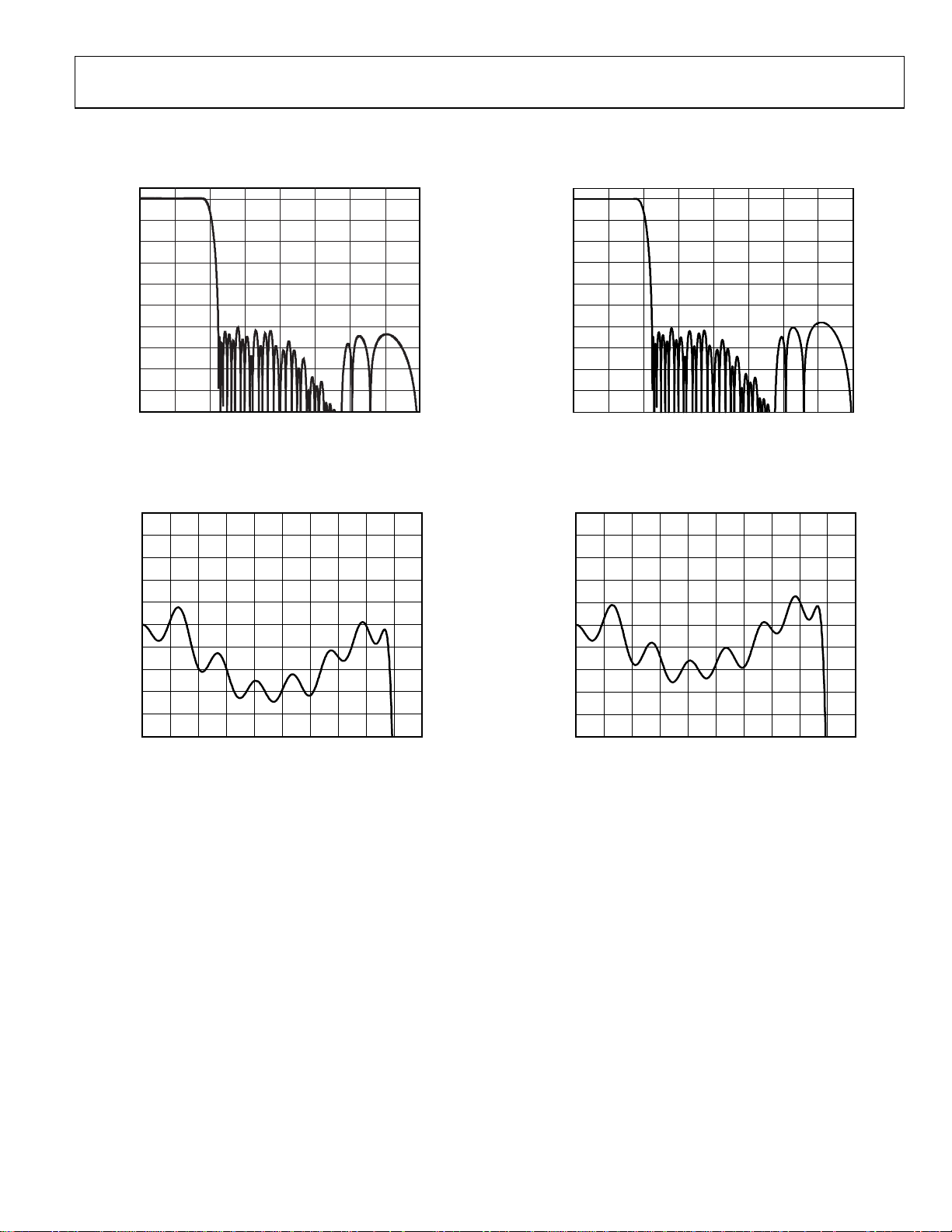
Pass Band 0 0.445 fS Hz ±0.04 dB
0.5 fS Hz −6 dB
Pass-Band Ripple ±0.04 dB
Stop Band 0.555 fS Hz
Stop-Band Attenuation −61 dB f > 0.567 fS
High-Pass Filter Corner Frequency 3.7 Hz −3 dB
10.4 Hz −0.5 dB
21.6 Hz −0.1 dB
DAC FILTER
Pass Band 0 0.445 fS Hz ±0.04 dB
0.5 fS Hz −6 dB
Pass-Band Ripple ±0.04 dB
Stop Band 0.555 fS Hz
Stop-Band Attenuation −61 dB f > 0.565 fS
CORE CLOCK TOLERANCE
Frequency Range 8.0 13.8 MHz
Jitter Tolerance 50 ps
Rev. 0 | Page 4 of 28
SSM2604
TIMING CHARACTERISTICS
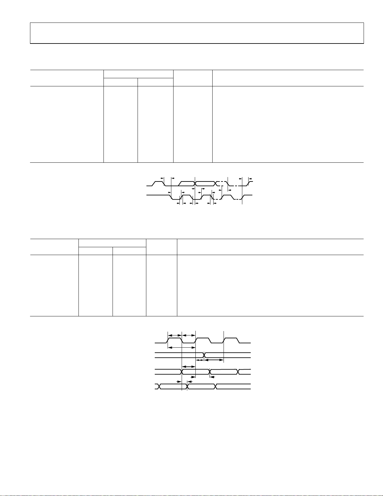
Table 3. I2C Timing
Limit
Parameter t
t
600 ns Start condition setup time
SCS
t
600 ns Start condition hold time
SCH
tPH 600 ns SCLK pulse width high
tPL 1.3 µs SCLK pulse width low
f
0 526 kHz SCLK frequency
SCLK
tDS 100 ns Data setup time
tDH 900 ns Data hold time
tRT 300 ns SDIN and SCLK rise time
tFT 300 ns SDIN and SCLK fall time
t
600 ns Stop condition setup time
HCS
t
MIN
Unit Description
MAX
SDIN
SCLK
t
t
PL
t
RT
SCH
t
DS
Figure 2. I
t
PH
t
DH
2
C Timing
t
HCS
t
SCS
t
FT
06978-036
Table 4. Digital Audio Interface Slave Mode Timing
Parameter t
Limit
t
MIN
MAX
Unit Description
tDS 10 ns PBDAT setup time from BCLK rising edge
tDH 10 ns PBDAT hold time from BCLK rising edge
t
10 ns RECLRC/PBLRC setup time to BCLK rising edge
LRSU
t
10 ns RECLRC/PBLRC hold time to BCLK rising edge
LRH
tDD 30 ns RECDAT propagation delay from BCLK falling edge (external load of 70 pF)
t
25 ns BCLK pulse width high
BCH
t
25 ns BCLK pulse width low
BCL
t
50 ns BCLK cycle time
BCY
t
t
BCL
BCH
BCLK
PBLRC/
RECLRC
PBDAT
RECDAT
t
BCY
t
DS
t
t
LRSU
LRH
t
t
DD
DH
06978-025
Figure 3. Digital Audio Interface Slave Mode Timing
Rev. 0 | Page 5 of 28
SSM2604
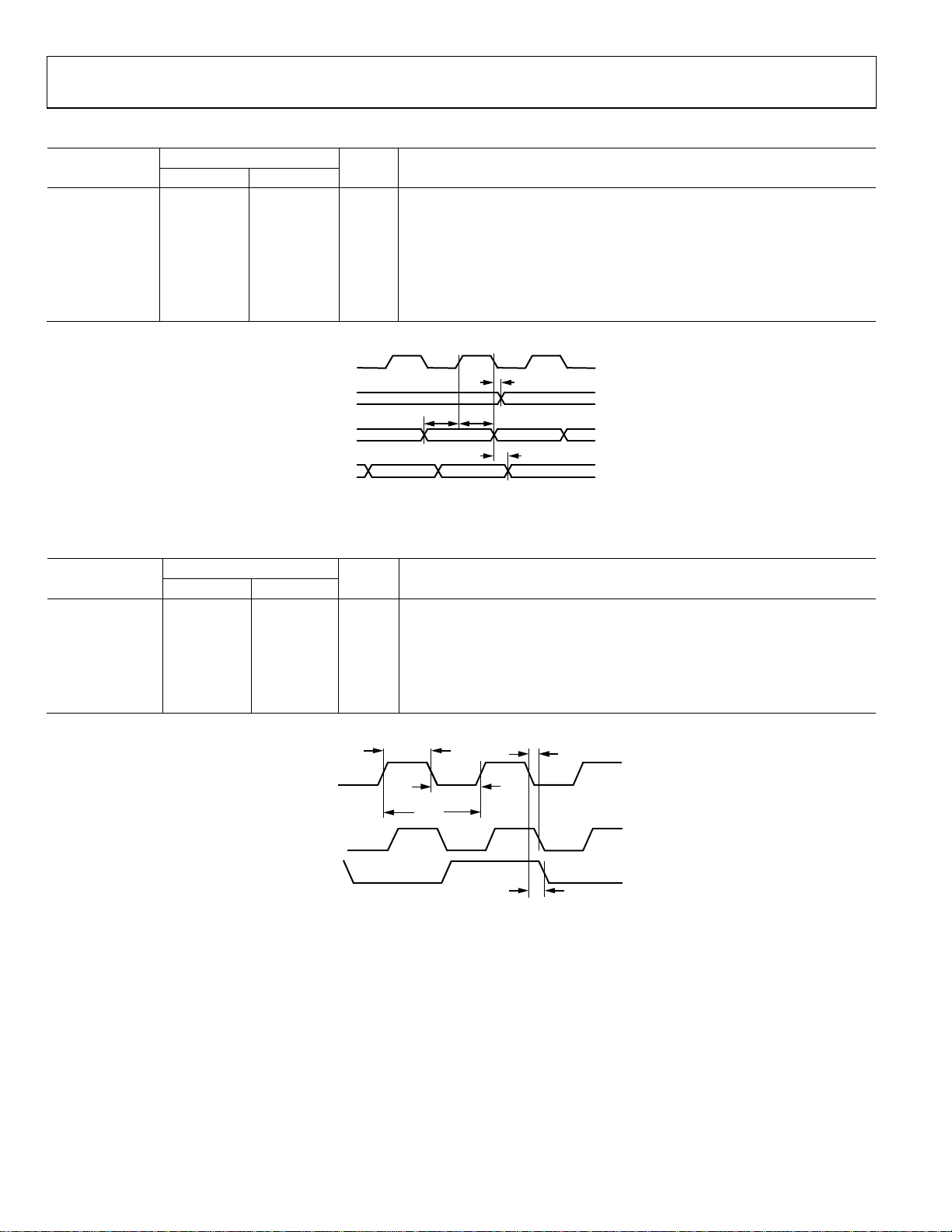
Table 5. Digital Audio Interface Master Mode Timing
Parameter t
t
30 ns PBDAT setup time to BCLK rising edge
DST
t
10 ns PBDAT hold time to BCLK rising edge
DHT
MIN
Limit
t
Unit Description
MAX
tDL 10 ns RECLRC/PBLRC propagation delay from BCLK falling edge
t
10 ns RECDAT propagation delay from BCLK falling edge
DDA
t
10 ns BCLK rising time (10 pF load)
BCLKR
t
10 ns BCLK falling time (10 pF load)
BCLKF
t
45:55:00 55:45:00 BCLK duty cycle (normal and USB mode)
BCLKDS
BCLK
t
PBLRC/
RECLRC
PBDAT
RECDAT
t
DSTtDHT
Figure 4. Digital Audio Interface Master Mode Timing
DL
t
DDA
6978-026
Table 6. System Clock Timing
Limit
Parameter t
t
72 ns MCLK/XTI system clock cycle time
XTIY
t
40:60 60:40:00 MCLK/XTI duty cycle
MCLKDS
t
32 ns MCLK/XTI system clock pulse width high
XTIH
t
32 ns MCLK/XTI system clock pulse width low
XTIL
t
20 ns CLKOUT propagation delay from MCLK/XTI falling edge
COP
t
20 ns CLKODIV2 propagation delay from MCLK/XTI falling edge
COPDIV2
t
MIN
Unit Description
MAX
MCLK/XTI
CLKOUT
CLKODI V2
t
XTIH
t
XTIL
t
XTIY
t
COPDIV2
Figure 5. System (MCLK) Clock Timing
t
COP
06978-035
Rev. 0 | Page 6 of 28
SSM2604
ABSOLUTE MAXIMUM RATINGS
At 25°C, unless otherwise noted.
Table 7.
Parameter Rating
Supply Voltage 3.6 V
Input Voltage VDD
Common-Mode Input Voltage VDD
Storage Temperature Range −65°C to +150°C
Operating Temperature Range −40°C to +85°C
Junction Temperature Range −65°C to +165°C
Lead Temperature (Soldering, 60 sec) 300°C
Stresses above those listed under Absolute Maximum Ratings
may cause permanent damage to the device. This is a stress
rating only; functional operation of the device at these or any
other conditions above those indicated in the operational
section of this specification is not implied. Exposure to absolute
maximum rating conditions for extended periods may affect
device reliability.
THERMAL RESISTANCE
θJA is specified for the worst-case conditions, that is, a device
soldered in a circuit board for surface-mount packages.
Table 8. Thermal Resistance
Package Type θJA θJC Unit
20-Lead, 4 mm × 4 mm LFCSP 28 32 °C/W
ESD CAUTION
Rev. 0 | Page 7 of 28
SSM2604
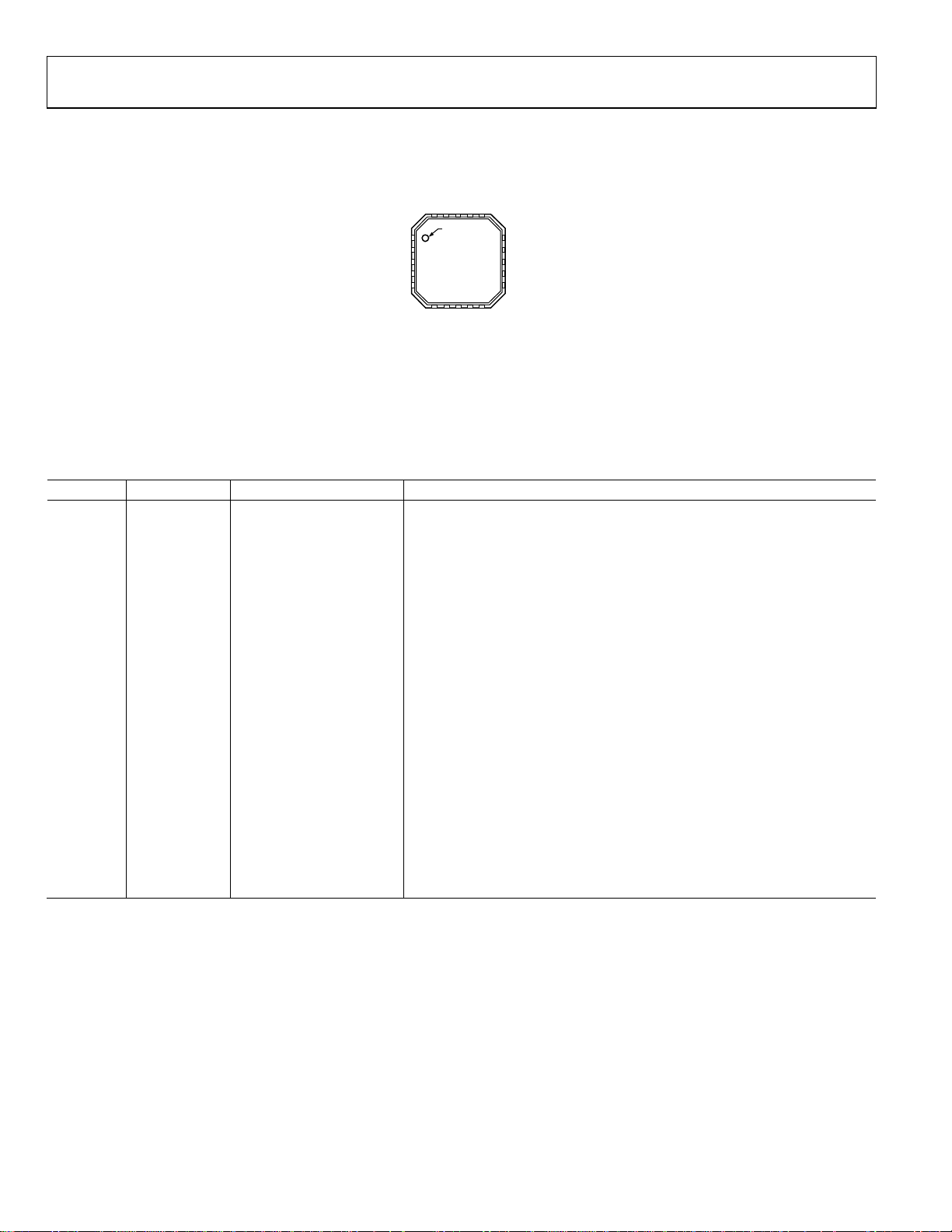
PIN CONFIGURATION AND FUNCTION DESCRIPTIONS
SDIN
SCLK
NC
LLINEIN
RLINEIN
17
16
18
19
20
PIN 1
INDICATOR
1MCLK/XTI
2XTO
SSM2604
3DGND
TOP VIEW
4DVDD
(Not to Scale)
5CLKOUT
6
7
CLK
B
NOTES
1. NC = NO CONNE CT.
2. FOR PROPER CONNECTION OF THE EXPOSED PAD,
CONNECT TO PCB GROUND LAYER
PBDAT
Figure 6. Pin Configuration
Table 9. Pin Function Descriptions
Pin No. Mnemonic Type Description
1 MCLK/XTI Digital Input Master Clock Input/Crystal Input.
2 XTO Digital Output Crystal Output.
3 DGND Digital Ground Digital Ground.
4 DVDD Digital Supply Digital Core and I/O Buffer Supply.
5 CLKOUT Digital Output Buffered Clock Output.
6 BCLK Digital Input/Output Digital Audio Bit Clock.
7 PBDAT Digital Input DAC Digital Audio Data Input, Playback Function.
8 PBLRC Digital Input/Output DAC Sampling Rate Clock, Playback Function (from Left and Right Channels).
9 RECDAT Digital Output ADC Digital Audio Data Output, Record Function.
10 RECLRC Digital Input/Output ADC Sampling Rate Clock, Record Function (from Left and Right Channels).
11 LOUT Analog Output Line Output for Left Channel.
12 ROUT Analog Output Line Output for Right Channel.
13 AVDD Analog Supply Analog Supply.
14 AGND Analog Ground Analog Ground.
15 VMID Analog Output Midrail Voltage Decoupling Input.
16 RLINEIN Analog Input Line Input for Right Channel.
17 LLINEIN Analog Input Line Input for Left Channel.
18 SDIN Digital Input/Output 2-Wire Control Interface Data Input/Output.
19 SCLK Digital Input 2-Wire Control Interface Clock Input.
20 NC NC No Connection
GND Pad Thermal Pad/Exposed Pad Center Thermal Pad. Connect to PCB ground layer.
15 VMID
14 AGND
13 AVDD
12 ROUT
11 LOUT
9
8
10
RC
PBL
RECLRC
RECDAT
06978-002
Rev. 0 | Page 8 of 28
SSM2604
TYPICAL PERFORMANCE CHARACTERISTICS
CONVERTER FILTER RESPONSE
0
–10
–20
–30
–40
–50
–60
MAGNITUDE (dB)
–70
–80
–90
–100
00.25
0.75 1.00 1.250.50 1.50 2.00
FREQUENCY (
f
)
S
Figure 7. ADC Digital Filter Frequency Response
0.05
0.04
0.03
0.02
0.01
0
−0.01
MAGNITUDE (dB)
−0.02
−0.03
−0.04
−0.05
0 0.050.100.150.200.250.300.350.400.450.50
FREQUENCY (
f
)
S
Figure 8. ADC Digital Filter Ripple
1.75
0
–10
–20
–30
–40
–50
–60
MAGNITUDE (dB)
–70
–80
–90
–100
00.25
06978-003
0.75 1.00 1.250.50 1.50 2.001.75
FREQUENCY (
f
)
S
6978-005
Figure 9. DAC Digital Filter Frequency Response
0.05
0.04
0.03
0.02
0.01
0
−0.01
MAGNITUDE (d B)
−0.02
−0.03
−0.04
−0.05
0 0.050.100.150.200.250.300.350.400.450.50
6978-004
FREQUENCY (
f
)
S
6978-006
Figure 10. DAC Digital Filter Ripple
Rev. 0 | Page 9 of 28
 Loading...