Analog Devices SMP04EP, SMP04EQ, SMP04ES Datasheet

CMOS Quad
a
FEATURES
Four Independent Sample-and-Holds
Internal Hold Capacitors
High Accuracy: 12 Bit
Very Low Droop Rate: 2 mV/s typ
Output Buffers Stable for C
TTL/CMOS Compatible Logic Inputs
Single or Dual Supply Applications
Monolithic Low Power CMOS Design
APPLICATIONS
Signal Processing Systems
Multichannel Data Acquisition Systems
Automatic Test Equipment
Medical and Analytical Instrumentation
Event Analysis
DAC Deglitching
≤ 500 pF
L
Sample-and-Hold Amplifier
SMP04*
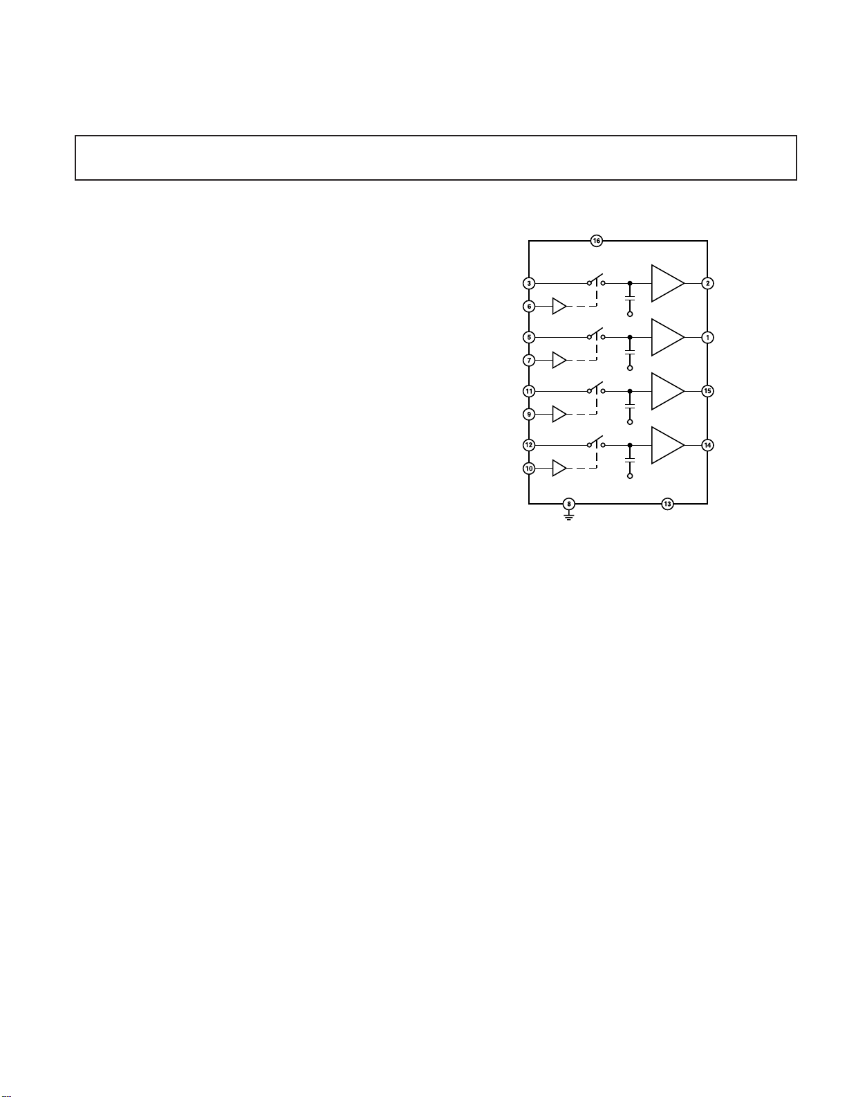
FUNCTIONAL BLOCK DIAGRAM
V
DD
SMP04
V
S/H
V
S/H
V
S/H
V
S/H
IN1
1
V
SS
IN2
2
V
SS
IN3
3
IN4
4
V
SS
V
SS
V
V
V
V
OUT1
OUT2
OUT3
OUT4
GENERAL DESCRIPTION
The SMP04 is a monolithic quad sample-and-hold; it has four
internal precision buffer amplifiers and internal hold capacitors.
It is manufactured in ADI’s advanced oxide isolated CMOS
technology to obtain the high accuracy, low droop rate and fast
acquisition time required by data acquisition and signal processing systems. The device can acquire an 8-bit input signal to
±1/2 LSB in less than four microseconds. The SMP04 can
operate from single or dual power supplies with TTL/CMOS
logic compatibility. Its output swing includes the negative supply.
The SMP04 is ideally suited for a wide variety of sample-andhold applications, including amplifier offset or VCA gain adjustments. One or more can be used with single or multiple DACs
to provide multiple setpoints within a system.
V
DGND
SS
The SMP04 offers significant cost and size reduction over
equivalent module or discrete designs. It is available in a
16-lead hermetic or plastic DIP and surface mount SOIC
packages. It is specified over the extended industrial tem-
perature range of –40°C to +85°C.
*Protected by U.S. Patent No. 4,739,281.
REV. D
Information furnished by Analog Devices is believed to be accurate and
reliable. However, no responsibility is assumed by Analog Devices for its
use, nor for any infringements of patents or other rights of third parties
which may result from its use. No license is granted by implication or
otherwise under any patent or patent rights of Analog Devices.
One Technology Way, P.O. Box 9106, Norwood, MA 02062-9106, U.S.A.
Tel: 781/329-4700 World Wide Web Site: http://www.analog.com
Fax: 781/326-8703 © Analog Devices, Inc., 1998

SMP04–SPECIFICATIONS
ELECTRICAL CHARACTERISTICS
(@ VDD = +12.0 V, VSS = DGND = 0 V, RL = No Load, TA = Operating Temperature Range
specified in Absolute Maximum Ratings, unless otherwise noted.)
Parameter Symbol Conditions Min Typ Max Units
Linearity Error 0.01 %
V
Buffer Offset Voltage V
Hold Step V
Droop Rate ∆V/∆tV
Output Source Current
Output Sink Current
1
1
OS
HS
I
SOURCE
I
SINK
Output Voltage Range OVR R
LOGIC CHARACTERISTICS
Logic Input High Voltage V
Logic Input Low Voltage V
Logic Input Current I
DYNAMIC PERFORMANCE
Acquisition Time
Acquisition Time
Hold Mode Settling Time t
Slew Rate
3
3
4
2
Capacitive Load Stability C
INH
INL
IN
t
AQ
t
AQ
H
SR R
L
Analog Crosstalk 0 V to 10 V Step –80 dB
SUPPLY CHARACTERISTICS
Power Supply Rejection Ratio PSRR 10.8 V ≤ V
Supply Current I
Power Dissipation P
DD
DIS
= 6 V –10 ±2.5 +10 mV
IN
VIN = 6 V, T
= 6 V, T
V
IN
= 6 V, T
IN
= +25°C to +85°C2.54mV
A
= –40°C5mV
A
= +25°C 2 25 mV/s
A
VIN = 6 V 1.2 mA
VIN = 6 V 0.5 mA
= 20 kΩ 0.06 10.0 V
L
R
= 10 kΩ 0.06 9.5 V
L
2.4 V
0.8 V
0.5 1 µA
T
= +25°C, 0 V to 10 V Step to 0.1% 3.5 4.25 µs
A
–40°C ≤ T
T
= +25°C, 0 V to 10 V Step to 0.01% 9 µs
A
≤ +85°C 3.75 5.25 µs
A
To 1 mV 1 µs
= 20 kΩ 34 V/µs
L
<30% Overshoot 500 pF
≤ 13.2 V 60 75 dB
DD
47 mA
84 mW
ELECTRICAL CHARACTERISTICS
(@ VDD = +5.0 V, VSS = –5.0 V, DGND = 0.0 V, RL = No Load, TA = Operating Temperature
Range specified in Absolute Maximum Ratings, unless otherwise noted.)
Parameter Symbol Conditions Min Typ Max Units
Linearity Error 0.01 %
V
Buffer Offset Voltage V
Hold Step V
OS
HS
Droop Rate ∆V/∆tV
Output Resistance R
Output Source Current
Output Sink Current
1
1
OUT
I
SOURCE
I
SINK
Output Voltage Range OVR R
LOGIC CHARACTERISTICS
Logic Input High Voltage V
Logic Input Low Voltage V
Logic Input Current I
DYNAMIC PERFORMANCE
Acquisition Time
Acquisition Time
Hold Mode Settling Time t
Slew Rate
3
3
5
2
Capacitive Load Stability C
INH
INL
IN
t
AQ
t
AQ
H
SR R
L
SUPPLY CHARACTERISTICS
Power Supply Rejection Ratio PSRR ±5 V ≤ V
Supply Current I
Power Dissipation P
NOTES
1
Outputs are capable of sinking and sourcing over 20 mA, but linearity and offset are guaranteed at specified load levels.
2
All input control signals are specified with tR = tF = 5 ns (10% to 90% of +5 V) and timed from a voltage level of 1.6 V.
3
This parameter is guaranteed without test.
4
Slew rate is measured in the sample mode with a 0 V to 10 V step from 20% to 80%.
5
Slew rate is measured in the sample mode with a –3 V to +3 V step from 20% to 80%.
Specifications are subject to change without notice.
DD
DIS
= 0 V –10 ±2.5 +10 mV
IN
VIN = 0 V, T
= 0 V, T
V
IN
= 0 V, T
IN
= +25°C to +85°C2.54mV
A
= –40°C5mV
A
= +25°C 2 25 mV/s
A
1 Ω
VIN = 0 V 1.2 mA
VIN = 0 V 0.5 mA
= 20 kΩ –3.0 +3.0 V
L
2.4 V
0.8 V
0.5 1 µA
–3 V to +3 V Step to 0.1% 3.6 11 µs
–3 V to +3 V Step to 0.01% 9 µs
To 1 mV 1 µs
= 20 kΩ 3V/µs
L
<30% Overshoot 500 pF
≤ ±6 V 60 75 dB
DD
3.5 5.5 mA
55 mW
–2–
REV. D

SMP04
ABSOLUTE MAXIMUM RATINGS
(T
= +25°C unless otherwise noted)
A
VDD to DGND . . . . . . . . . . . . . . . . . . . . . . . . . . . –0.3 V, 17 V
V
to VSS . . . . . . . . . . . . . . . . . . . . . . . . . . . . . –0.7 V, 17 V
DD
to DGND . . . . . . . . . . . . . . . . . . . . . . . . –0.3 V, V
V
LOGIC
VIN to DGND . . . . . . . . . . . . . . . . . . . . . . . . . . . . . . VSS, V
V
to DGND . . . . . . . . . . . . . . . . . . . . . . . . . . . . . VSS, V
OUT
DD
DD
DD
Analog Output Current . . . . . . . . . . . . . . . . . . . . . . . ±20 mA
(Not Short-Circuit Protected)
Digital Input Voltage to DGND . . . . . . . –0.3 V, V
+ 0.3 V
DD
Operating Temperature Range
EQ, EP, ES . . . . . . . . . . . . . . . . . . . . . . . . –40°C to +85°C
Junction Temperature . . . . . . . . . . . . . . . . . . . . . . . . .+150°C
Storage Temperature . . . . . . . . . . . . . . . . . . –65°C to +150°C
Lead Temperature (Soldering, 60 sec) . . . . . . . . . . . .+300°C
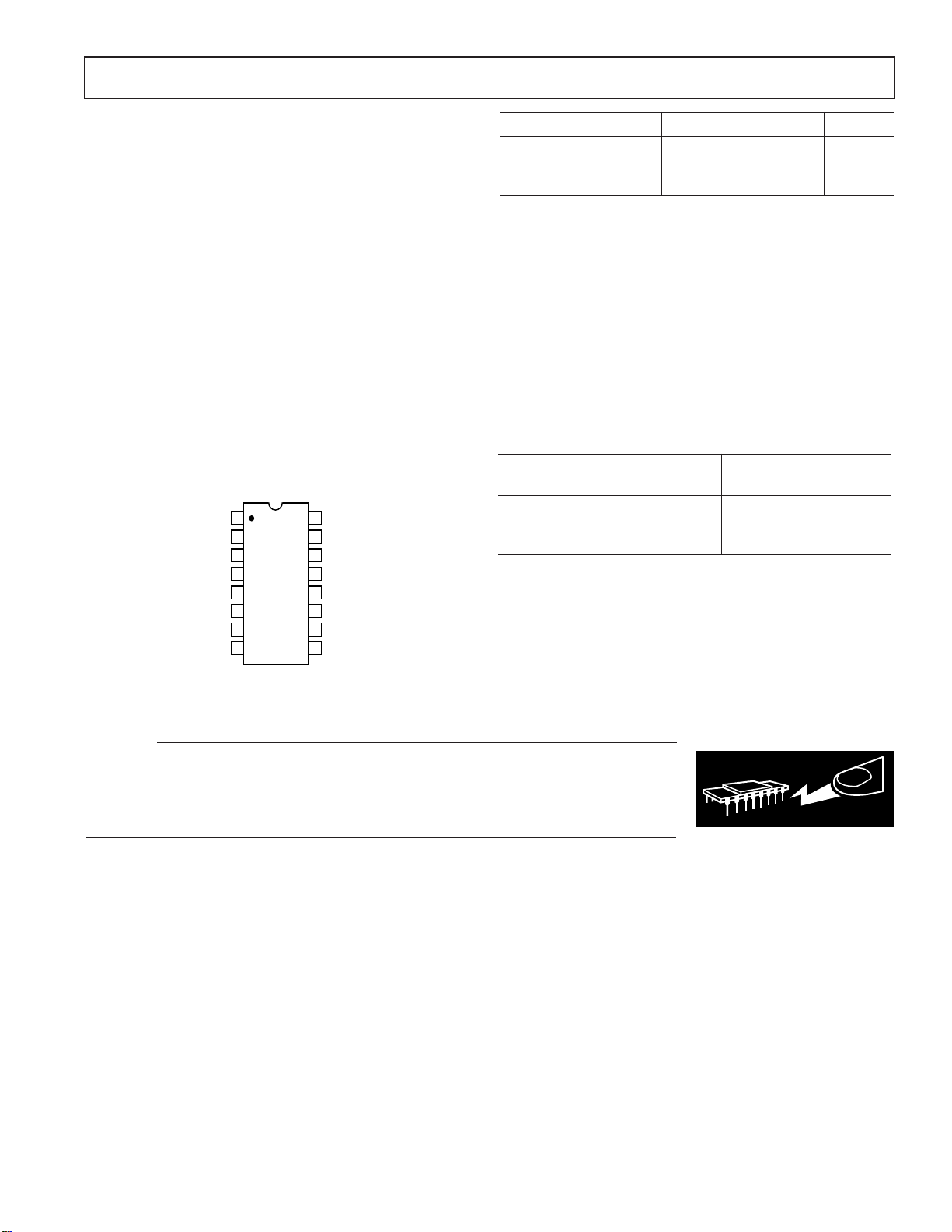
PIN CONNECTIONS
16-Lead Cerdip
16-Lead Plastic DIP
16-Lead SO
V
1
OUT2
2
V
OUT1
3
V
IN1
NC
4
V
5
IN2
S/H
6
1
S/H
7
2
DGND
8
NC = NO CONNECT
SMP04
TOP VIEW
(Not to Scale)
V
16
DD
V
15
OUT3
V
14
OUT4
V
13
SS
V
12
IN4
V
11
IN3
10
S/H
4
9
S/H
3
Package Type JA*
JC
Units
16-Lead Cerdip 94 12 °C/W
16-Lead Plastic DIP 76 33 °C/W
16-Lead SO 92 27 °C/W
*JA is specified for worst case mounting conditions, i.e., JA is specified for device
in socket for cerdip and plastic DIP packages;
to printed circuit board for SO package.
is specified for device soldered
JA
CAUTION
1. Stresses above those listed under Absolute Maximum Ratings may cause
permanent damage to the device. This is a stress rating only; function operation
at or above this specification is not implied. Exposure to the above maximum
rating conditions for extended periods may affect device reliability.
2. Digital inputs and outputs are protected; however, permanent damage may
occur on unprotected units from high energy electrostatic fields. Keep units in
conductive foam or packaging at all times until ready to use. Use proper antistatic
handling procedures.
3. Remove power before inserting or removing units from their sockets.
ORDERING GUIDE
Temperature Package Package
Model Range Description Options*
SMP04EQ –40°C to +85°C Cerdip-16 Q-16
SMP04EP –40°C to +85°C PDIP-16 N-16
SMP04ES –40°C to +85°C SO-16 R-16A
*Q = Cerdip; N = Plastic DIP; R = Small Outline.
CAUTION
ESD (electrostatic discharge) sensitive device. Electrostatic charges as high as 4000 V readily
accumulate on the human body and test equipment and can discharge without detection.
Although the SMP04 features proprietary ESD protection circuitry, permanent damage may
occur on devices subjected to high energy electrostatic discharges. Therefore, proper ESD
precautions are recommended to avoid performance degradation or loss of functionality.
WARNING!
ESD SENSITIVE DEVICE
REV. D
–3–

SMP04
OUT2
DGND
2
V
V
OUT3
DD
V
OUT4
S/H3S/H
V
SS
V
IN4
V
IN3
4
V
V
S/H
V
IN1
IN2
1
OUT1
V
S/H
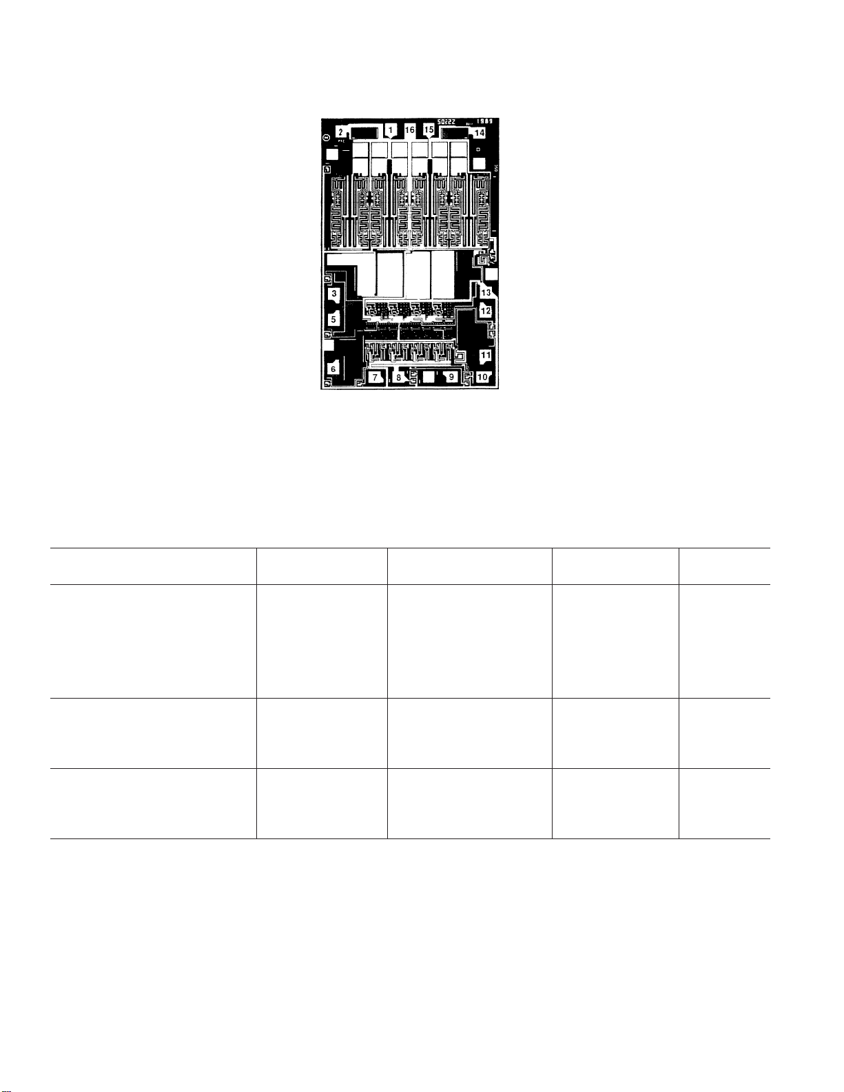
Dice Characteristics
Die Size: 0.80 x 0.120 mil = 9,600 sq. mil
(2.032 x 3.048mm = 6.193 sq. mm)
WAFER TEST LIMITS
(@ VDD = +12 V, VSS = DGND = 0 V, RL = No Load, TA = +25ⴗC, unless otherwise noted.)
SMP04G
Parameter Symbol Conditions Limits Units
V
Buffer Offset Voltage V
Hold Step V
OS
HS
Droop Rate ∆V/∆tV
Output Source Current I
Output Sink Current I
SOURCE
SINK
Output Voltage Range OVR R
= +6 V ±10 mV max
IN
V
= +6 V ±4 mV max
IN
= +6 V 25 mV/s max
IN
VIN = +6 V 1.2 mA min
VIN = +6 V 0.5 mA min
= 20 kΩ 0.06/10.0 V min/max
L
R
= 10 kΩ 0.06/9.5 V min/max
L
LOGIC CHARACTERISTICS
Logic Input High Voltage V
Logic Input Low Voltage V
Logic Input Current I
INH
INL
IN
2.4 V min
0.8 V max
1 µA max
SUPPLY CHARACTERISTICS
Power Supply Rejection Ratio PSRR 10.8 V ≤ V
Supply Current I
Power Dissipation P
NOTE
Electrical tests are performed at wafer probe to the limits shown. Due to variations in assembly methods and normal yield loss, yield after packaging is not guaranteed
for standard product dice. Consult factory to negotiate specifications based on dice lot qualifications through sample lot assembly and testing.
DD
DIS
≤ 13.2 V 60 dB min
DD
7 mA max
84 mW max
–4–
REV. D

Typical Performance Characteristics–SMP04
INPUT VOLTAGE – Volts
DROOP RATE – mV/s
1800
1200
600
01 10
23456789
1600
1400
1000
800
VDD = +12V
V
SS
= 0V
10000
VDD = +12V
V
= 0V
SS
VIN = +5V
1000
= 10kV
R
L
100
DROOP RATE – mV/s
10
0
–55 –35 125
–15 5 25 65 85 10545
TEMPERATURE – 8C
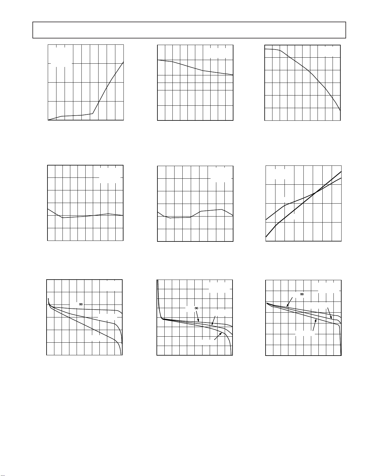
Figure 1. Droop Rate vs. Temperature
3
2
1
0
–1
HOLD STEP – mV
–2
TA = +258C
V
= +12V
DD
V
= 0V
SS
5
3
1
0
–1
DROOP RATE – mV/s
–3
–5
01 10
23456789
INPUT VOLTAGE – Volts
VDD = +12V
V
= 0V
SS
Figure 2. Droop Rate vs. Input
Voltage (T
3
2
1
0
–1
HOLD STEP – mV
–2
= +25°C)
A
VDD = +12V
V
= 0V
SS
V
= +5V
IN
Figure 3. Droop Rate vs. Input
Voltage (T
7
TA = +258C
VSS = 0V
6
5
SLEW RATE – V/ms
4
= +125°C)
A
–SR
+SR
–3
01 10
23456789
INPUT VOLTAGE – Volts
Figure 4. Hold Step vs. Input Voltage
2
1
0
–1
–2
OFFSET VOLTAGE – mV
–3
–4
01 10
RL =
23456789
INPUT VOLTAGE – Volts
RL = 20kV
RL = 10kV
VDD = +12V
V
= 0V
SS
Figure 7. Offset Voltage vs. Input
Voltage (T
= +25°C)
A
–3
–55 –35 125
–15 5 25 65 85 10545
TEMPERATURE – 8C
Figure 5. Hold Step vs. Temperature
20
15
10
5
0
–5
–10
OFFSET VOLTAGE – mV
–15
–20
01 10
RL =
23456789
INPUT VOLTAGE – Volts
VDD = +12V
V
RL = 10kV
= 0V
SS
RL = 20kV
Figure 8. Offset Voltage vs. Input
Voltage (T
= +125°C)
A
3
10 11 18
Figure 6. Slew Rate vs. V
4
2
0
–2
–4
–6
OFFSET VOLTAGE – mV
–8
–10
12 13 14 15 16 17
V
– Volts
DD
DD
VDD = +12V
V
= 0V
RL =
RL = 10kV
01 10
23456789
INPUT VOLTAGE – Volts
SS
RL = 20kV
Figure 9. Offset Voltage vs. Input
Voltage (T
= –55°C)
A
REV. D
–5–
 Loading...