

Page 1

Engineer-to-Engineer Note EE-236
a
Technical notes on using Analog Devices DSPs, processors and development tools
Contact our technical support at dsp.support@analog.com and at dsptools.support@analog.com
Or vi sit our o n-li ne r esou rces htt p:/ /www.analog.com/ee-notes and http://www.analog.com/processors
Real-Time Solutions Using Mixed-Signal Front-End Devices with the
Blackfin® Processor
Contributed by Prashant Khullar Rev 1 – May 18, 2004
Introduction
Certain areas of telecommunications
infrastructure are evolving towards the creation
of smaller, localized wireless networks. These
so-called ‘picocells’ can extend wireless
connectivity to areas where terrestrial networks
are not present. The development of this microinfrastructure brings about the need for compact
devices that can perform some of the tasks
traditionally associated with larger wireless base
stations.
The Blackfin® family of processors can be
gluelessly integrated with a mixed-signal frontend (MxFE) for these and a wide variety of other
real-time applications. The Blackfin
architecture’s signal processing performance,
ease of programmability, and flexible parallel
port make it an ideal candidate for such roles.
Additionally, MxFE devices integrate the
necessary analog front-end functionality onto a
single chip with a programmable architecture.
Hardware Architecture
The AD9866 MxFE is chosen for this discussion.
The 12-bit data converters (A/D and D/A) on the
MxFE connect to the Blackfin’s parallel
peripheral interface (PPI) without any external
logic. The PPI is a half-duplex 16-bit parallel
port which runs at up to half the speed of the
Blackfin system clock (SCLK/2). At the
maximum SCLK frequency of 133 MHz, this
translates to a PPI update rate of 66 MHz. The
MxFE serial interface for control register
configuration connects directly to the Blackfin’s
serial peripheral interface (SPI). Depending on
the application’s bandwidth requirements, a halfduplex or full-duplex implementation can be
used. The former can be accomplished using the
ADSP-BF531/BF532/BF533 line of processors
which have a single PPI.
Full-duplex applications require a dual
!
PPI device such as the ADSP-BF561
symmetric multiprocessor. Such
implementations are not discussed in
this EE-Note.
As shown in Figure 1, the parallel digital
interfaces of the 12-bit ADC and 12-bit DAC
connect directly to the Blackfin PPI. A fixed
number of samples is transferred directly using
DMA from the ADC to a buffer in the
processor’s internal memory. Signal processing
may then be performed on this block of data
before the PPI direction is reversed and the data
is transferred out to the DAC.
General-purpose flag pins are used to alternately
enable and disable the ADC and DAC in a
deterministic fashion. All data transfers are
synchronized by a single clock sourced by an
oscillator running at frequencies up to 60 MHz.
Copyright 2004, Analog Devices, Inc. All rights reserved. Analog Devices assumes no responsibility for customer product design or the use or application of
customers’ products or for any infringements of patents or rights of others which may result from Analog Devices assistance. All trademarks and logos are property
of their respective holders. Information furnished by Analog Devices applications and development tools engineers is believed to be accurate and reliable, however
no responsibility is assumed by Analog Devices regarding technical accuracy and topicality of the content provided in Analog Devices’ Engineer-to-Engineer Notes.
Page 2
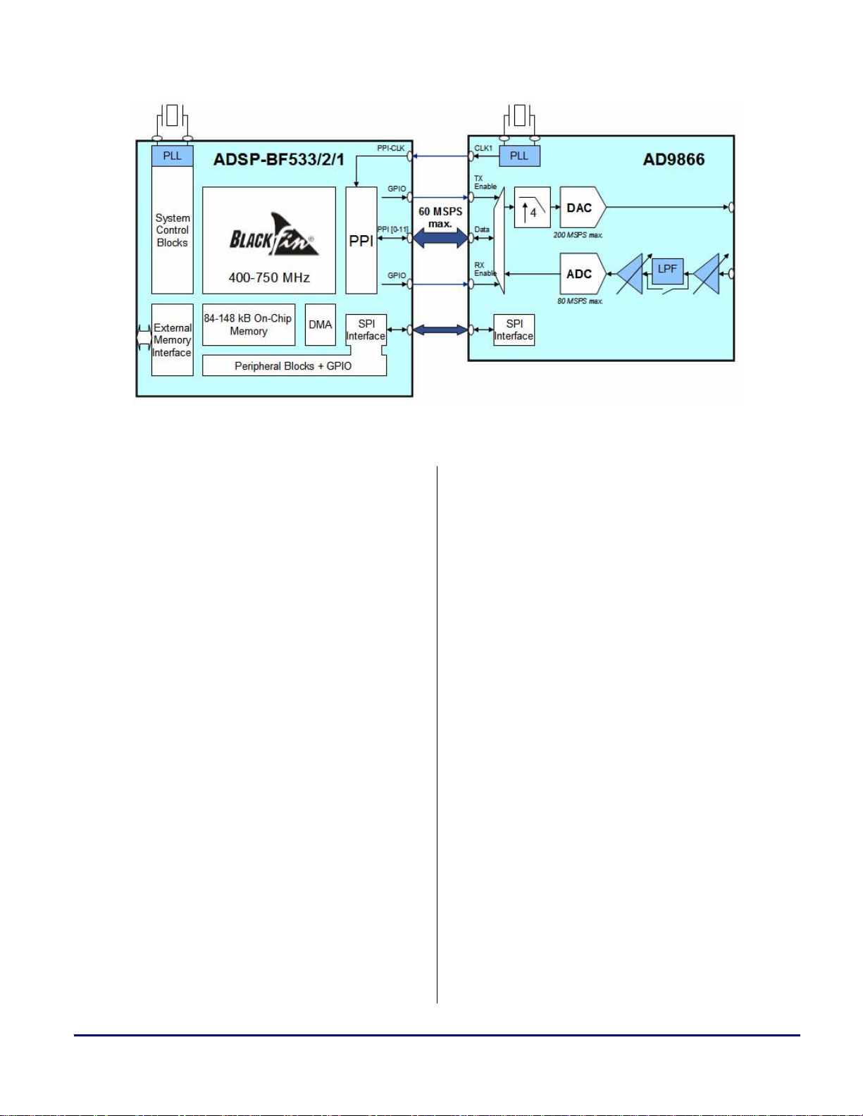
Figure 1. Hardware Interconnection
a
The serial connection between the Blackfin and
AD9866 is used to program the MxFE’s onboard register set. These registers control various
aspects of the device’s operation including power
management, clocking, programmable gain
amplifiers, and interpolation filters.
Software-Controlled Data Flow
To implement such a half-duplex communication
scheme, the PPI and DMA controller on the
Blackfin processor need to reverse their direction
of data transfer at specified intervals. This can be
accomplished in software using a block of
configuration code placed in an interrupt service
routine (ISR). In the tested implementation, a
general-purpose timer was used to generate the
interrupts that trigger this routine at deterministic
intervals. The timer period was chosen
empirically such that the time between
successive interrupts was adequate to ensure that
the ongoing DMA transfer is able to complete
and that the ‘turnaround’ code is also able to
execute to completion.
the main execution flow and the ISR. The delay
involved with reconfiguring the GPIO, DMA,
and PPI register sets constitutes the remainder of
the turn-around time.
The subsequent quantitative analysis of this
dataflow uses the following abbreviations:
N: Number of Samples (Data Window
Size)
CCLK: Blackfin Core Clock Frequency
SCLK: Blackfin System Clock Frequency
DCLK: Data Clock/PPI Clock (synchronizes
MxFE converters and PPI)
RX 0, RX 1: first and second halves of the received
data window, respectively
TX 0, TX 1: first and second halves of the
transmitted data window, respectively
P0, P1: signal processing of first and second
data window halves, respectively
The following benchmarks were obtained
empirically:
The latency associated with the DMA/PPI turnaround code has two components. The first is the
time associated with switching context between
Real-Time Solutions Using Mixed-Signal Front-End Devices with the Blackfin® Processor (EE-236) Page 2 of 5
Context Switch Latency (Using EX_InterruptHandler with
the stack in L1 Data Memory) =
ISR Initialization Latency +
Page 3

a
ISR Termination Latency =
32 CCLK cycles
GPIO/DMA/PPI Reconfiguration Latency =
25 SCLK + 73 CCLK cycles
(223 CCLK cycles at a 6:1 SCLK:CCLK ratio)
Total Turn-around Latency =
25 SCLK cycles + 105 CCLK cycles
(255 CCLK cycles at a 6:1 SCLK:CCLK ratio)
To boost processing efficiency, a ping-pong
scheme is implemented in software, whereby
ADSP-BF533
PPI
DMA
Core
Bus
MxFE
Converters
PPI_Data
[11:0]
DMA
Access
Bus
(DAB)
(DCB)
DMA
signal processing tasks may be performed in
parallel with DMA transfers. In particular, input
and output data buffers are broken into halves so
that one half may be processed while the other is
being read or written by the DMA controller.
The following data-flow diagram and execution
timeline illustrate this half-duplex ping-pong
scheme.
Core Processing
RX 0
Load
Data
DCB
L1 Internal Memory Buffers
RX 1
TX 0
TX 1
Store
Data
Figure 2. Digital Dataflow
Figure 3. Execution Timeline
Real-Time Solutions Using Mixed-Signal Front-End Devices with the Blackfin® Processor (EE-236) Page 3 of 5
Page 4

a
For applications that require larger and
!
As demonstrated above, the turn-around latency
reduces the available bandwidth minimally. The
maximum throughput of this arrangement can be
quantified as follows.
With CCLK = 750 MHz, SCLK = 125 MHz,
DCLK = 60 MHz:
Turnaround Latency =
255 CCLK cycles ≈ 20 DCLK cycles
Average bandwidth lost to turn-around latency =
[1/(20 DCLK cycles)]*2 Bytes =
(DCLK/20)*2 Bytes = 6 megabytes/second
Average RX Throughput = Average TX Throughput =
[(DCLK/2) – (DCLK/20)]*2 Bytes
= 54 megabytes/second
variably-sized sample windows, the
above data flow can be modified easily
to place buffers in external SDRAM.
Signal Processing
The real-time processing workload that can be
accommodated depends on the size of the data
window. The time taken by the algorithm to
complete must not exceed the deterministic time
required for the parallel DMA transfer to
complete. Appropriate selection of the window
size is therefore essential. In general, signal
processing algorithms that execute slower than in
linear time become unmanageable as the window
size grows large. On the other hand, algorithms
that execute faster than in linear time may be
more efficient to implement with large window
sizes. The demonstrational example used to test
this system performed a 512-point Fast Fourier
Transform (FFT) followed by an inverse FFT of
the same size on each half of the 1024-sample
window. Both algorithms execute slower than in
linear time (O(n log n)); therefore they can be
expected to exceed the available processing time
if the data window size is increased indefinitely.
Half-Duplex Synchronization
using flag pins. The Blackfin processor acts as
the master device by toggling flag pins
connected to the Transmit Enable (TXEN) and
Receive Enable (RXEN) pins of the AD9866.
The active-high RXEN and TXEN signals
indicate when valid data is being read from the
ADC or written to the DAC by the Blackfin PPI,
respectively. These signals are not transmitted
over the analog medium. Therefore, in this halfduplex scheme, an external device connected to
the analog medium needs to be able to handle the
alternating bursts of data transmission and
reception.
One possible implementation is for the device to
have built-in circuitry to distinguish between
valid data and silence. A simple dead-band
circuit, which enables data sampling after a
certain analog voltage threshold is exceeded,
would be appropriate. Additionally, the device
would need to be programmed to receive and
transmit data bursts of a pre-specified length.
When interfacing to external devices that require
explicit data framing, the TXEN and RXEN
signals can be transmitted alongside the analog
signals.
Implementation
The hardware components and configuration
required to evaluate this design are outlined in
the
VisualDSP++® project that accompanies this
EE-Note. A glueless 3-board interconnection is
required. The AD9866 Evaluation Board
connects directly to the ADSP-BF533/BF561
EZ-Extender card, which interfaces to the
ADSP-BF533 EZ-KIT Lite™ Evaluation Board.
The VisualDSP++ software module that
demonstrates the hardware’s functionality is
written entirely in embedded C. It provides a
proof-of-concept with enough flexibility and
modularity to fit a wide range of applications.
readme.txt file included in the
Data transfers between the AD9866’ high-speed
converters and the Blackfin PPI are synchronized
Real-Time Solutions Using Mixed-Signal Front-End Devices with the Blackfin® Processor (EE-236) Page 4 of 5
Page 5

a
Conclusion
With bidirectional throughput of over 50
megabytes/second, a flexible programming
model, and ample processing headroom, the halfduplex interconnection of a Blackfin processor
and MxFE is particularly well-suited to low-cost
wireless infrastructure. Moreover, it is general
enough to be used for any number of real-time
applications.
References
[1] ADSP-BF533 Blackfin Processor Hardware Reference. Revision 1.0, November 2003, Analog Devices Inc.
[2] AD9866 12-bit Broadband Modem Mixed Signal Front End Datasheet. Revision 0.0, November 2003.
Analog Devices Inc.
Document History
Revision Description
Rev 1 – May 18, 2004
by P. Khullar
Initial Release
Real-Time Solutions Using Mixed-Signal Front-End Devices with the Blackfin® Processor (EE-236) Page 5 of 5
 Loading...