

Page 1

Engineer-to-Engineer Note EE-223
a
Technical notes on using Analog Devices DSPs, processors and development tools
Contact our technical support at dsp.support@analog.com and at dsptools.support@analog.com
Or vi sit our o n-li ne r esou rces htt p:/ /www.analog.com/ee-notes and http://www.analog.com/processors
Programming In-Circuit Flash on the ADSP-21262 SHARC® DSP
Contributed by R Murphy Rev 1 – January 23, 2004
Introduction
The ADSP-21262 SHARC® DSP, like most reprogrammable processors, requires internal program
code and data to be boot-loaded upon power-up. The
code and data can be supplied by a host system (e.g.,
via SPI, JTAG connection, etc.) or can be stored in an
on-board non-volatile memory device such as a ROM
or in a serial or parallel flash device. The ADSP21262 EZ-KIT Lite™ evaluation board enables the
DSP to boot in any of these ways. The focus of this
Engineer-to-Engineer note is PROM booting. This is
supported by an 8-Mbit flash memory device
(AM29LV081B-120EC) from AMD.
The system designer and the EZ-KIT Lite user alike
have several options available to program the boot
code into the flash device.
Flash Programmer Utility
VisualDSP++® 3.0 for SHARC DSPs includes a
Flash Programmer utility that allows you to point the
flash utility to a previously programmed loader
(.LDR) file and programs the flash based on a
supplied driver file. The driver file is simply a DSP
executable (.DXE) developed for a specific processor
and flash device combination. The VisualDSP++
development tools include a driver file for the ADDS21262 EZ-KIT Lite board, allowing you to program
your own driver file with your own specific flash
device.
Attached Example Code
Alternatively, the Flash Programmer utility itself can
be circumvented, and the attached example code can
be used to manually program the image into flash.
This is useful for verifying the development of a
custom driver for the Flash Programmer utility as
well as for simply creating a custom executable for
use in programming the end system.
This example shows how the VisualDSP++ can be
used to program an application into the flash. “Incircuit programming” (as opposed to burning the
flash before it is placed on the board) is frequently
used to perform software or firmware updates to
systems already deployed in the field.
The task requires two separate sets of code: a
software routine to program data into the flash, and
an end application that will ultimately be boot-loaded
and run by the DSP. In this example, a generic flash
programming algorithm is contained in
flash_programmer.asm, and the application is a
simple LED toggling routine in
blink.asm. (This
routine will serve as the data payload that
flash_programmer.asm will program into the
flash.) The attached code example demonstrates the
four steps involved with in-circuit flash
programming.
Overview
1. Building the Application
Using the USB Debug Agent, a JTAG emulator,
and/or the VisualDSP++ simulator, you can write and
test the application. As previously mentioned, the
application in
sequentially. Verify that this routine and your board
is functional by activating an EZ-KIT Lite debugtarget in the IDDE and then opening
Next, load the
executable has been loaded, run the project (press the
<F5> key) and watch the LEDs.
blink.asm toggles LED0-LED8
blink.dpj.
blink.dxe executable. After the
Copyright 2004, Analog Devices, Inc. All rights reserved. Analog Devices assumes no responsibility for customer product design or the use or application of
customers’ products or for any infringements of patents or rights of others which may result from Analog Devices assistance. All trademarks and logos are property
of their respective holders. Information furnished by Analog Devices Applications and Development Tools Engineers is believed to be accurate and reliable, however
no responsibility is assumed by Analog Devices regarding technical accuracy and topicality of the content provided in Analog Devices’ Engineer-to-Engineer Notes.
Page 2
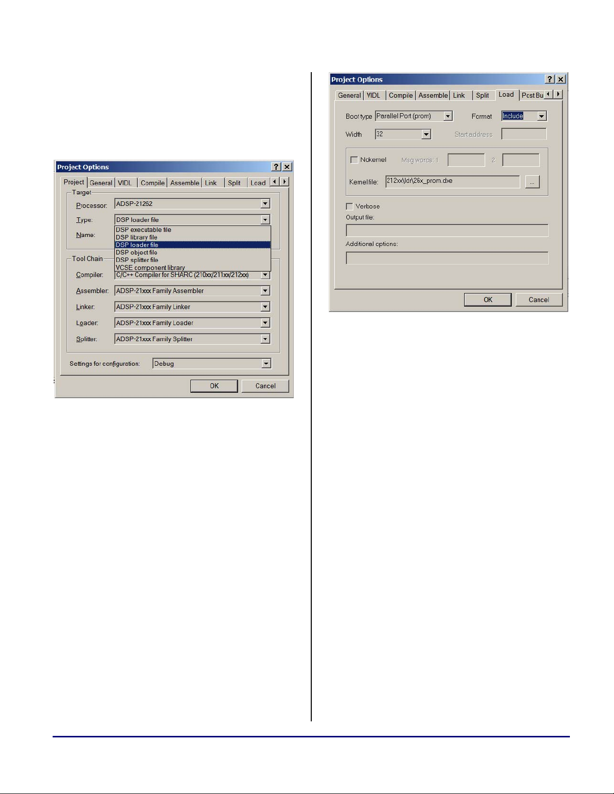
2. Creating the PROM Boot-Image
After verifying the application, use the VisualDSP++
loader to generate a boot-image from the source code.
To do this, open the Project Options dialog box for
blink.dpj and specify “DSP loader file” as the
output file type (Figure 1.)
Figure 2. Specifying Parallel Port (prom) as boot type
a
Figure 1. Specifying DSP loader file as output file type
The .LDR file to be generated will ultimately be
included in the flash-programming routine as an
array. To this end, the .LDR file should be in
“Include” format (essentially comma-delimited
ASCII) with each word being 32-bits, as shown in
Figure 2.
Click "OK" and then click "Rebuild All". This
rebuilds the project according to the specified project
options and generates
3. Programming the Flash Device
At this point, use the Flash Programmer utility (A) or
included flash-programmer project (B) to program the
.LDR image into the flash device.
blink.ldr.
3A. Using the Flash Programmer Utility
i. From the VisualDSP++ Tools menu, choose
‘Flash Programmer’.
ii. Click on ‘Load Driver’. The utility will load a
supplied driver for the AMD Flash on the EZKIT Lite board (or you can browse to a custom
flash driver file).
iii. Browse to the folder containing blink.ldr and
click ‘Load File’
iv. In the ‘Confirm Load File’ dialog box, click
‘Yes’.
v. When the status icon turns green, reset the board
to boot the new application code.
3B. Using the Included flash_programmer Project
i. Open
ii. Rebuild the project with your application code.
flash_programmer.dpj.
The last step is to modify the flash-programming
application to include the recently generated
blink.ldr. To do this, in the file
flash_programmer.asm, simply declare an
array in a section mapped to external memory and
initialize it with the payload .LDR file. To use the
example application (blink), this is done as
follows:
Programming In-Circuit Flash on the ADSP-21262 SHARC® DSP Page 2 of 13
Page 3

.section/dm seg_ext8;
.var my_file[]= "blink.ldr";
The linker description file (.LDF) is then used to
pack all
memory seg ment (also named
With the correct payload file specified, simply
rebuild the project to generate the flashprogramming executable.
(flash_programmer.dxe) .
iii. Programming the FLASH
Four LEDs provide feedback on the progress of
the FLASH programming.As each of the
following five steps to program the FLASH
complete, an LED illuminates to indicate that it
was successful or blinks rapidly if it failed.
The five steps are as follows:
seg_ext8 input sections to an external
seg_ext8).
1. Verify that the payload fits into the 1 M x 8-
bit Flash.
2. Reset the flash.
3. Erase the flash (completely or by-sector).
4. Write the payload .LDR file into the FLASH.
5. Verify the data.
If all five steps are successful, all of the LEDs briefly
flash, indicatinge that the in-circuit FLASH
programming was successful. You may now reset the
board and the new application code will be booted.
Additional Notes
In this example, the payload buffer,
my_file[], is initiated at build time. In a real
system, this buffer would be initialized during
execution. The FLASH data may be imported
from a serial port, link port, or SPI port. The data
could be placed into memory by an on-board
host processor.
Viewing the flash and external memory space via
memory windows in the IDDE is supported in
VisualDSP++ 3.0 using the HP PCI ICE.
However, during debug of the application, this
may cause the debugger window to hang
momentarily, especially while single stepping.
To avoid this bottleneck, close the external
memory windows while the code is running, and
open them as needed to verify the memory
contents.
a
References
[1] ADSP-2126x SHARC DSP Core Manual, Revision 1.0, November 2003. Analog Devices, Inc.
[2]
ADSP-2126x SHARC DSP Peripherals Manual, Revision 1.0, December 2003. Analog Devices, Inc.
[3] ADSP-21262 EZ-KIT Lite® Evaluation System Manual, Revision 1.0, October 2003. Analog Devices, Inc.
[4] ADSP-21262 SHARC Processor Preliminary Data Sheet, Revision PrB, August 2003. Analog Devices, Inc.
[5] AM29LV081B 1M x 8-Bit Uniform Sector Flash Memory Data Sheet, Revision D, September 2003. AMD
Programming In-Circuit Flash on the ADSP-21262 SHARC® DSP Page 3 of 13
Page 4

a
Appendix
flash_programmer.asm
/* ********************************************************************************
*
* Copyright (c) 2003 Analog Devices Inc. All rights reserved.
*
* *******************************************************************************/
//"flash_programmer.asm" RJM 9/2003 DSP Applications Engineering
//This program is intended for the AMD 8-bit 1M parallel flash
//found on the ADSP-21262 Ez-Kit.
//The subroutines will:
// -FLASH_FILE_SIZE: -check to see that the buffer 'my_file' is not too large to
// fit in the 1Mx8 flash
// -FLASH_RESET: -issue the flash reset command
// -ERASE_FLASH_CHIP; -erase the entire flash and wait until the erase command is
// completed
// -SECTOR_ERASE: -calculate the number of sector needed to hold the data and
// -erase accordingly (and verify erasure)
// -PROGRAM_FLASH: -program the flash with the data/code in my_file and check
// for write cmd completion after each byte
// -VERIFY_FLASH: -verify the contents of the flash with the values in
// ‘my_file'
//This example is intended to provide a starting point to be tailored to fit
//specific needs.
//The VERIFY_FLASH routine can be omitted and you can use either SECTOR_ERASE or
//ERASE_FLASH_CHIP
//External memory (SRAM) is not required to store the data before programming, but
//is desirable if the data is > internal memory.
//***Be advised, initializing a large un-initialized variable in external memory
//can take a long time to load with the emulator.
//***For debug purposes, after loading the external segment once, use the
//SHT_NOBITS command in the LDF to avoid this lengthy process
//***as you debug. Be sure to rebuild without SHT_NOBITS after debug.
//To program boot loader code into the flash, use the Loader in VisualDSP++ 3.0 SP1
//to generate a .ldr file with the following options:
// -Width: 32
// -Boot Type: Parallel Port (prom)
// -Format: Include
//
//*************************************************
#include <def21262.h>
#define FLASH_START_ADDRESS 0x01000000
#define FLASH_SIZE 0x100000
#define LED_ADDRESS 0x01400000
#define SRAM_START_ADDRESS 0x01200000
#define SECTOR_SIZE 65536
#define NUMBER_SECTORS (LENGTH(my_file)*BYTES >>16) +1
//i.e. if length of file in bytes is 0x1ffff, 1 sector= 0xffff, shift by 16 gives
//us 1+1 etc.
#define BYTES 4 //i.e. 4 * 8bits = 32 bit logical data width
// 2 * 8bits = 16 bit logical data width
// 1 * 8bits = 8 bit logical data width
.global main;
Programming In-Circuit Flash on the ADSP-21262 SHARC® DSP Page 4 of 13
Page 5

.section/dm seg_dmda;
.var LED_value;
.var External_Byte_Address;
.var External_Sector_Address[]=0;
.var Data_Byte;
.var External_Byte_Address_Sram;
.var Swap;
.var Word_To_Write[2];
.var Word_Read_In[2];
.section/dm seg_ext8; //external SRAM 512k xin the ADSP-21262
//EZ-Kit Lite
//.var my_file[65536]; //a blank array for demonstration purposes
.var my_file[]= "blink.ldr"; //to use a file to hold the programming data
.section/pm seg_pmco;
main:
nop;
bit set mode1 IRPTEN; nop; //Global Interrupt Enable
bit set LIRPTL PPIMSK; nop; //The Parallel Port interrupt is the only one
//used
nop;nop;nop;
//Status Lights
r4=1; call WRITE_TO_LEDS; //LED1 lit at start
call SETUP;
r4=3; call WRITE_TO_LEDS; //LED2 lit after erase command
call PROGRAM_FLASH;
r4=0x7; call WRITE_TO_LEDS; //LED4 lit after flash programmed
call VERIFY_FLASH;
r4=0xf; call WRITE_TO_LEDS; //LED5 lit after verified successfully
jump DONE;
SETUP:
call FLASH_FILE_SIZE; //be sure the data will fit in the flash
call FLASH_RESET; //issue the flash reset command
call SECTOR_ERASE; //erases proper # of sectors and verifies erasure
rts;
main.end:
ERASE_FLASH_CHIP:
r0 = 0x55aa0000; nop; //this is the CHIP ERASE Command for the AMD 29LV081B
dm(Word_To_Write) = r0; nop;
r0 = 0x1055aa80; nop;
dm(Word_To_Write+1) = r0; nop;
// init DMA reg's
r0 = Word_To_Write; dm(IIPP)=r0; nop;
r0=1; dm(IMPP)=r0; nop;
r0=4; dm(ICPP)=r0; nop;
r0 = FLASH_START_ADDRESS; dm(EIPP)=r0; nop;
r0=0; dm(EMPP)=r0; nop;
a
Programming In-Circuit Flash on the ADSP-21262 SHARC® DSP Page 5 of 13
Page 6

r0=8; dm(ECPP)=r0; nop;
ustat1= PPTRAN| // transmit
PPBHC| // bus hold cycle
PPDUR12;// data cycle duration of 12 core clock cycles
dm(PPCTL)=ustat1; nop;
// initiate DMA
bit set ustat1 PPDEN|PPEN;
dm(PPCTL)=ustat1; nop;
// wait for DMA to complete
idle;
r0=0;
dm(PPCTL)=r0; nop;
r0 = FLASH_START_ADDRESS;
dm(External_Byte_Address) = r0;
nop;
rts;
SECTOR_ERASE:
r1=65536-1; //Calculate second to last address of sector
r2=FLASH_START_ADDRESS;
r2=r2+r1; //create address within 1st sector
dm(External_Sector_Address) = r2; //first sector address
r0=NUMBER_SECTORS; //this loop erases and verifies one sector
//per iteration
lcntr=r0, do sectors until lce;
r0 = 0x55aa0000; nop; //this is the SECTOR ERASE Command for the
// AMD 29LV081B
dm(Word_To_Write) = r0; nop;
r0 = 0x3055aa80; nop;
dm(Word_To_Write+1) = r0; nop;
// init DMA reg's
r0 = Word_To_Write; dm(IIPP)=r0; nop;
r0=1; dm(IMPP)=r0; nop;
r0=4; dm(ICPP)=r0; nop;
r0 =dm(External_Sector_Address); dm(EIPP)=r0; nop;
//address of the sector
//we wish to erase this iteration
r0=0; dm(EMPP)=r0; nop;
r0=8; dm(ECPP)=r0; nop;
ustat1= PPTRAN| // transmit
PPBHC| // bus hold cycle
PPDUR12;// data cycle duration of 12 core clock cycles
dm(PPCTL)=ustat1; nop;
a
Programming In-Circuit Flash on the ADSP-21262 SHARC® DSP Page 6 of 13
Page 7

// initiate DMA
bit set ustat1 PPDEN|PPEN;
dm(PPCTL)=ustat1; nop;
// wait for DMA to complete
idle;
r0=0;
dm(PPCTL)=r0; nop;
nop;nop;
call FLASH_ERASED; //check if sector is erased
r1 = 65536;
r0 = dm(External_Sector_Address);
r0=r0+r1; //add for next sector
dm(External_Sector_Address) = r0;
sectors:nop;
nop;
nop;
rts;
FLASH_ERASED:// checks to see if the flash or sector was erased successfully
r2 = 0;
r0 = dm(External_Sector_Address);
dm(External_Byte_Address)=r0;
call READ_FLASH_WORD; //Check that the data at that address = 0xFF
r0 = dm(Word_Read_In); nop; //This indicates the flash is erased, but you
//wait until the
r1 = 0xFFFFFFFF; //data has stopped toggling so that you know
r1 = r0 - r1; //you are reading a flash location, not the
//flash's status register
if ne jump FLASH_ERASED;
nop;
rts;
PROGRAM_FLASH:
r0 = FLASH_START_ADDRESS;
dm(External_Byte_Address) = r0;
r0 = SRAM_START_ADDRESS;
dm(External_Byte_Address_Sram) = r0;
r0=LENGTH(my_file)*BYTES; //length of data in words * value in BYTES = #
//of 8-bit locations to verify
lcntr=r0, do PROGRAM_FLASH_LOOP until lce; //each loop iteration writes two
//8-bit flash locations
call READ_SRAM_WORD;
r6 = dm(Swap);
dm(Data_Byte) = r6;
call WRITE_FLASH_BYTE ; //write 8 bits of the data
r0 = dm(External_Byte_Address);
a
Programming In-Circuit Flash on the ADSP-21262 SHARC® DSP Page 7 of 13
Page 8

r0 = r0 + 1;
dm(External_Byte_Address) = r0; //update flash address for DMA
// in WRITE_FLASH_BYTE
r0 = dm(External_Byte_Address_Sram);
r0 = r0 + 1;
dm(External_Byte_Address_Sram) = r0; //update sram address for DMA
// in READ_SRAM_WORD
nop;
PROGRAM_FLASH_LOOP:
nop;
nop;
rts;
VERIFY_FLASH:
r0=FLASH_START_ADDRESS;
dm(External_Byte_Address)=r0;
r0=SRAM_START_ADDRESS;
dm(External_Byte_Address_Sram) = r0;
r0=LENGTH(my_file)*BYTES; //length of data in words * value in BYTES = # of
//8-bit locations to verify
lcntr=r0; do VERIFY until lce;
//fetch byte from flash
call READ_FLASH_WORD;
r7=dm(Word_Read_In);
r7=fext r7 BY 0:8;
//increment FLASH address
r1=dm(External_Byte_Address);
r1=r1+1;
dm(External_Byte_Address)=r1;
//fetch byte from source in SRAM
call READ_SRAM_WORD;
r15=dm(Swap);
r15 = fext r15 by 0:8;
//increment SRAM address
r1=dm(External_Byte_Address_Sram);
r1=r1+1;
dm(External_Byte_Address_Sram)=r1;
//compare
r15=r15-r7;
if ne jump TEST_FAIL;
//don't branch in last 3 instr of loop:
nop;
nop;
VERIFY: nop;
rts;
a
Programming In-Circuit Flash on the ADSP-21262 SHARC® DSP Page 8 of 13
Page 9

WRITE_FLASH_BYTE:
// init DMA reg's
r0=0;
dm(PPCTL)=r0;
r0 = 0x00000000; nop; //These several lines of code take the 8-bit
//data and combine it with
dm(Word_To_Write) = r0; nop; //the PROGRAM command word for the AMD flash,
//resulting in a 32-bit word to be issued to
//the flash using parallel port DMA
r3 = dm(Data_Byte); nop;
r3 = lshift r3 by 24; nop;
r0 = 0x00a055aa; nop;
r3 = r3 + r0; nop;
dm(Word_To_Write +1) = r3; nop;
r0 = Word_To_Write; dm(IIPP)=r0; nop;
r0=1; dm(IMPP)=r0; nop;
r0=4; dm(ICPP)=r0; nop;
r0 = dm(External_Byte_Address); dm(EIPP)=r0; nop;
r0=0; dm(EMPP)=r0; nop;
r0=8; dm(ECPP)=r0; nop;
ustat1= PPTRAN| // transmit
PPBHC| // bus hold cycle
PPDUR12; // data cycle duration of 12 core clock cycles
dm(PPCTL)=ustat1; nop;
// initiate DMA
bit set ustat1 PPDEN|PPEN;
dm(PPCTL)=ustat1; nop;
// wait for DMA to complete
idle;
nop;
call POLL_FLASH; //After issuing the program command and the data
//to be written, we cannot move on until
nop; //the program command algorithm is completed by
//the flash. When data read back
//does not toggle in 2 consecutive reads,the
//program command has completed successfully
r0=0;
dm(PPCTL)=r0;
rts;
READ_SRAM_WORD:
// init DMA reg's
r0=Swap; dm(IIPP)=r0; nop;
r0=1; dm(IMPP)=r0; nop;
r0=1; dm(ICPP)=r0; nop;
r0=dm(External_Byte_Address_Sram); dm(EIPP)=r0; nop;
r0=0; dm(EMPP)=r0; nop;
r0=4; dm(ECPP)=r0; nop;
a
Programming In-Circuit Flash on the ADSP-21262 SHARC® DSP Page 9 of 13
Page 10

ustat1= PPBHC| // bus hold cycle
PPDUR12; // data cycle duration of 12 core clock cycles
dm(PPCTL)=ustat1; nop;
// initiate DMA
bit set ustat1 PPDEN|PPEN;
dm(PPCTL)=ustat1; nop;
//wait for rx DMA to complete
idle;
r0=0;
dm(PPCTL)=r0;
nop;
nop;
nop;
nop;
rts;
READ_FLASH_WORD:
// init DMA reg's
r0=Word_Read_In; dm(IIPP)=r0; nop;
r0=1; dm(IMPP)=r0; nop;
r0=1; dm(ICPP)=r0; nop;
r0=dm(External_Byte_Address); dm(EIPP)=r0; nop;
r0=0; dm(EMPP)=r0; nop;
r0=4; dm(ECPP)=r0; nop;
ustat1= PPBHC| // bus hold cycle
PPDUR12; // data cycle duration of 12 core clock cycles
dm(PPCTL)=ustat1; nop;
// initiate DMA
bit set ustat1 PPDEN|PPEN;
dm(PPCTL)=ustat1; nop;
//wait for rx DMA to complete
idle;
r0=0;
dm(PPCTL)=r0;
nop;
nop;
nop;
nop;
rts;
FLASH_FILE_SIZE:
r5 = length(my_file)*BYTES; // read the # of bytes to program
r6 = 1024000; // size of flash is 1Mx8
comp (r5, r6);
a
Programming In-Circuit Flash on the ADSP-21262 SHARC® DSP Page 10 of 13
Page 11

if ge jump TEST_FAIL; // verify file will fit in flash
rts;
FLASH_RESET:
r0= 0xF0;//Command for RESET of FLASH
dm(Word_To_Write+1)=r0;
r0=Word_To_Write; dm(IIPP)=r0; nop;
r0=1; dm(IMPP)=r0; nop;
r0=2; dm(ICPP)=r0; nop;
r0 = dm(External_Byte_Address); dm(EIPP)=r0; nop;
r0=0; dm(EMPP)=r0; nop;
r0=8; dm(ECPP)=r0; nop;
ustat1= PPTRAN| // transmit
PPBHC| // bus hold cycle
PPDUR12; // data cycle duration of 12 core clock cycles
dm(PPCTL)=ustat1; nop;
// initiate DMA
bit set ustat1 PPDEN|PPEN;
dm(PPCTL)=ustat1; nop;
// wait for DMA to complete
idle;
nop;
r0=0;
dm(PPCTL)=r0;
rts;
POLL_FLASH: //After issuing the program command and the data
//to be written, we cannot move on until
r1 = 0; //the program command is completed by the flash.
//When data read back does not toggle
r2 = 0; //in 2 consecutive reads,the program command has
//completed successfully
call READ_FLASH_WORD;
r0 = dm(Word_Read_In); nop;
r1 = fext R0 BY 0:8;
r2 = fext R0 BY 8:8;
r1 = r1 - R2;
if ne jump POLL_FLASH;
nop;
rts;
WRITE_TO_LEDS: //The 8 user LEDs on the ADSP-21262 EZ-Kit are
//mapped to flag pins as well as the parallel
//port AD0-7 pins, so we can use a dma to write
//the latch to light the LEDs
// new LED value passed in via R4
dm(LED_value)=r4;
// init DMA reg's
r0=LED_value; dm(IIPP)=r0; nop;
a
Programming In-Circuit Flash on the ADSP-21262 SHARC® DSP Page 11 of 13
Page 12

r0=1; dm(IMPP)=r0; nop;
r0=1; dm(ICPP)=r0; nop;
r0=1; dm(EMPP)=r0; nop;
r0=0x01400000; dm(EIPP)=r0; nop;
r0=1; dm(ECPP)=r0; nop;
ustat1= PPTRAN| // transmit
PPBHC| // bus hold cycle
PPDUR12; // data cycle duration of 12 core clock cycles
dm(PPCTL)=ustat1; nop;
// initiate DMA
bit set ustat1 PPDEN|PPEN;
dm(PPCTL)=ustat1; nop;
// wait for DMA to complete
idle;
r0=0;
dm(PPCTL)=r0;
rts;
DONE:
r0 = 0x00FF0000;
dm(LED_value)=r0;
lcntr=20; do DONE_LOOP until lce; nop;
r4=dm(LED_value);
r4 = rot r4 by 16;
dm(LED_value)=r4;
Call WRITE_TO_LEDS;
lcntr=2250000; do Wait_Loop until lce; nop;
nop;
nop;
nop;
Wait_Loop:
nop;
nop;
nop;
DONE_LOOP:
nop;
END:
nop;
jump END;
TEST_FAIL:
nop;
jump TEST_FAIL;
a
Listing 1. flash_programmer.asm
Programming In-Circuit Flash on the ADSP-21262 SHARC® DSP Page 12 of 13
Page 13

Document History
Version Description
a
Rev 1 – January 23, 2004
by R. Murphy
Initial Release
Programming In-Circuit Flash on the ADSP-21262 SHARC® DSP Page 13 of 13
 Loading...