Circuit Note
6 GHz Ultrahigh Dynamic Range Differential
Amplifier
Rev. 0
engineers. Standard engineering practices have been employed in the design and construction of
room temperature. However, you are solely responsible for testing the circuit and determining its
suitability and applicability for your use and application. Accordingly, in no event shall Analog Devices
tal, consequential or punitive damages due to any cause
whatsoever connected to the use of any Circuits from the Lab circuits. (Continued on last page)
Fax: 781.461.3113 ©2012 Analog Devices, Inc. All rights reserved.
0.1µF
0.1µF
0.1µF
33pF
36nH
0.1µF
ADL5565
G = 12dB
2.5pF
XFMR
1:2 Z
TC2-1T
INPUT
Z = 50Ω
Z
I
= 100Ω
INTERNAL
INPUT Z
AD9642
14-BIT
205MSPS
ADC
620nH
5Ω
5Ω
187Ω40Ω217Ω
+3.3V
+1.8V
DRVDD
+1.8V
AVDD
5.6dB LOSS 0.2dB LOSS
5.8dB LOSS
11.8dB GAI N
FS = 1.75V
p-p DIFF
620nH
0.5dB LOSS
ANALOG
INPUT
+1.5dBm FS
AT 127MHz
OVERALL
GAIN = 5.5dB
100Ω
100Ω
0.1µF
5Ω
5Ω
15Ω
15Ω
2.85kΩ
1.2pF
1.2pF
33pF
VCM
36nH
VIP2
VIN2
VIP1
VIN1
10823-001
Circuits from the Lab™ reference circuits are engineered and
tested for quick and easy system integration to help solve today’s
analog, mixed-signal, and RF design challenges. For more
information and/or support, visit www.analog.com/CN0279.
High IF Sampling Receiver Front End with Band-Pass Filter
EVALUATION AND DESIGN SUPPORT
Design and Integration Files
Schematics, Layout Files, Bill of Materials
CIRCUIT FUNCTION AND BENEFITS
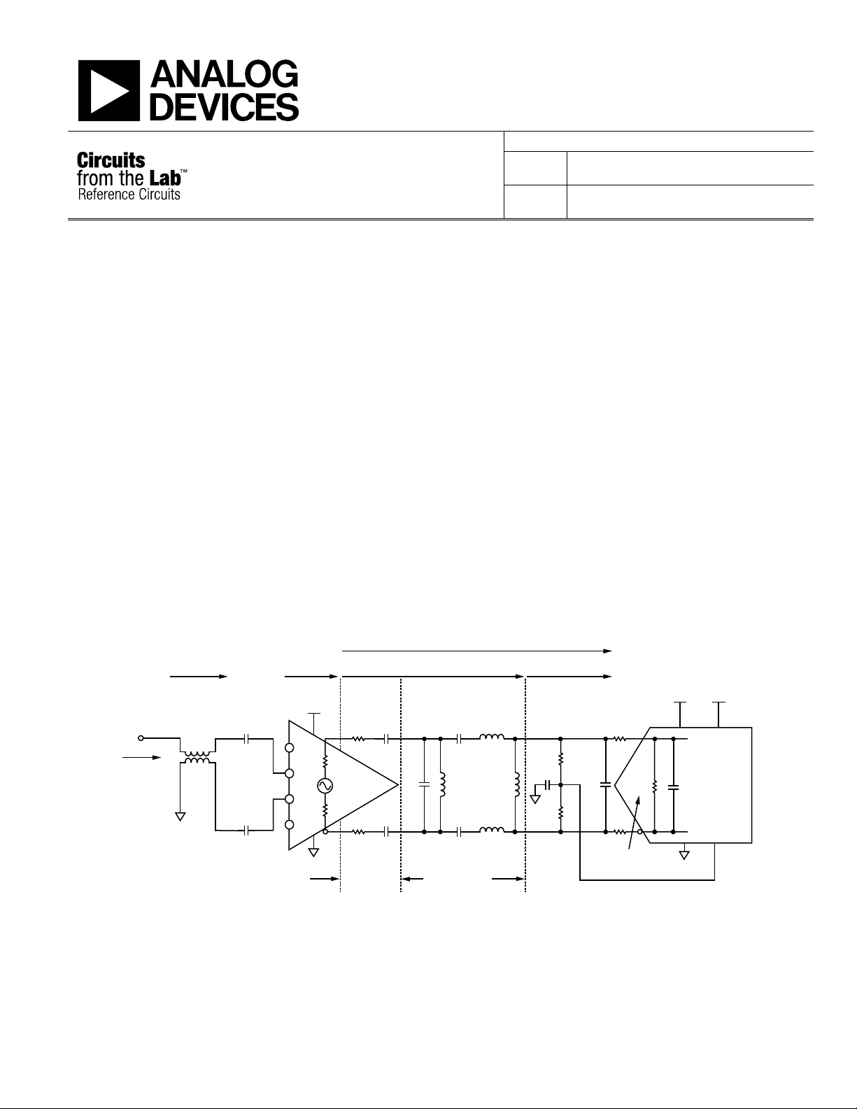
The circuit, shown in Figure 1, is a narrow, band-pass receiver
front end based on the ADL5565 ultralow noise differential
amplifier driver and the AD9642 14-bit, 250 MSPS analog-todigital converter (ADC).
The third-order, Butterworth antialiasing filter is optimized based
on the performance and interface requirements of the amplifier
and ADC. The total insertion loss due to the filter network and
other components is only 5.8 dB.
The overall circuit has a bandwidth of 18 MHz with a pass-band
flatness of 3 dB. The signal-to-noise ratio (SNR) and spuriousfree dynamic range (SFDR) measured with a 127 MHz analog
input are 71.7 dBFS and 92 dBc, respectively. The sampling
frequency is 205 MSPS, thereby positioning the IF input signal
in the second Nyquist zone between 102.5 MHz and 205 MHz.
CN-0279
Devices Connected/Referenced
AD9642 14-Bit, 250 MSPS Analog-to-Digital Converter
ADL5565
CIRCUIT DESCRIPTION
The circuit accepts a single-ended input and converts it to
differential input using a wide bandwidth (3 GHz) Mini-Circuits
TC2-1T 1:2 transformer. The 6 GHz ADL5565 differential
amplifier has a differential input impedance of 200 Ω when
operating at a gain of 6 dB, and 100 Ω when operating at a
gain of 12 dB. A gain option of 15.5 dB is also available.
The ADL5565 is an ideal driver for the AD9642, and the fully
differential architecture through the band-pass filter and into
the ADC provides good high frequency common-mode rejection,
as well as minimizes second-order distortion products. The
ADL5565 provides a gain of 6 dB or 12 dB, depending on the input
connection. In the circuit, a gain of 12 dB was used to compensate
for the insertion loss of the filter network and transformer
(approximately 5.8 dB), providing an overall signal gain of 5.5 dB.
Circuits from the Lab™ circuits from Analog Devices have been designed and built by Analog Devices
each circuit, and their function and performance have been tested and verified in a lab environment at
be liable for direct, indirect, special, inciden
Figure 1. 14-Bit, 250 MSPS Wideband Receiver Front End (Simplified Schematic: All Connections and Decoupling Not Shown)
Gains, Losses, and Signal Levels Measured Values for an Input Frequency of 127 MHz
One Technology Way, P.O. Box 9106, Norwood, MA 02062-9106, U.S.A.
Tel: 781.329.4700
www.analog.com

CN-0279 Circuit Note
39.8pF
(2.53pF)
0.987pF
(2.53pF)
0.987pF
39.5nH 39.8pF
100Ω
200Ω
(620nH)
1.59µH
(620nH)
1.59µH
100Ω
+
–
39.5nH
10443-002
–40
–35
–30
–25
–20
–15
–10
–5
0
AMPLITUDE (dBFS)
ANALOG I NP UT FREQUENCY (MHz)
50 250200150100 300
10823-003
50
55
60
65
70
75
80
85
90
95
118 120 122 124 126 128 130 132 134 136
SNR (dBFS) , SFDR (dBc)
ANALOG I NP UT FREQUENCY (MHz)
SNR (dBFS)
SFDR (dBc)
10823-004
An input signal of 1.5 dBm produces a full-scale 1.75 V p-p
differential signal at the ADC input.
The antialiasing filter is a third-order, Butterworth filter designed
with a standard filter design program. A Butterworth filter was
chosen because of its pass-band flatness. A third-order filter
yields an ac noise bandwidth ratio of 1.05 and can be designed
with the aid of several free filter programs such as Nuhertz
Technologies Filter Free, or the quite universal circuit simulator
(Qucs) free simulation.
To achieve best performance, load the ADL5565 with a net
differential load of 200 Ω. The 15 Ω series resistors isolate the
filter capacitance from the amplifier output, and the 100 Ω resistors
in parallel with the downstream impedance yield a net load
impedance of 217 Ω when added to the 30 Ω series resistance.
The 5 Ω resistors in series with the ADC inputs isolate internal
switching transients from the filter and the amplifier.
The 2.85 kΩ input impedance was determined using the downloadable spreadsheet on the AD9642 webpage. Simply use the
parallel track mode values at the center of the IF frequency of
interest. The spreadsheet shows both the real and imaginary values.
The third-order, Butterworth filter was designed with a source
impedance (differential) of 200 Ω, a load impedance (differential)
of 200 Ω, a center frequency of 127 MHz, and a 3 dB bandwidth
of 20 MHz. The calculated values from a standard filter design
program are shown in Figure 1. Because of the high values of
series inductance required, the 1.59 µH inductors were decreased
to 620 nH, and the 0.987 pF capacitors increased proportionally
to 2.53 pF, thereby maintaining the same resonant frequency of
127 MHz, with more realistic component values.
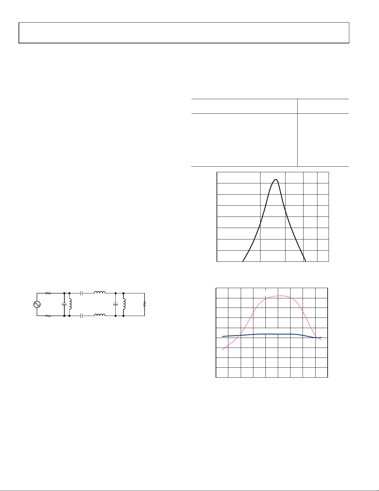
The measured performance of the system is summarized in
Table 1, where the 3 dB bandwidth, 18 MHz centered at 127 MHz.
The total insertion loss of the network is approximately 5.8 dB. The
frequency response is shown in Figure 3, and the SNR and SFDR
performance are shown in Figure 4.
Table 1. Measured Performance of the Circuit
Performance Specifications at −1 dBFS
(FS = 1.75 V p-p), Sample Rate = 205 MSPS
Final Results
Center Frequency 127 MHz
Pass-Band Flatness (118 MHz to 136 MHz) 3 dB
SNRFS at 127 MHz 71.7 dBFS
SFDR at 127 MHz 92 dBc
H2/H3 at 127 MHz 93 dBc/92 dBc
Overall Gain at 127 MHz 5.5 dB
Input Drive at 127 MHz 0.5 dBm (−1 dBFS)
Figure 3. Pass-Band Flatness Performance vs. Frequency
Figure 2. Starting Design for Third-Order, Differential Butterworth Filter with
Z
= 200 Ω, ZL = 200 Ω, FC = 127 MHz, and BW = 20 MHz
S
The internal 2.5 pF capacitance of the ADC was subtracted
from the value of the second shunt capacitor to yield a value of
37.3 pF. In the circuit, this capacitor was located near the ADC
to reduce/absorb the charge kickback.
The values chosen for the final filter passive components (after
adjusting for actual circuit parasitics) are shown in Figure 1.
Figure 4. SNR/SFDR Performance vs. Frequency, Sample Rate = 205 MSPS
Rev. 0 | Page 2 of 5
 Loading...