Circuit Note
CN-0260
10 MHz, 20 V/μs, G = 1, 10, 100, 1000 iCMOS®
Programmable Gain Instrumentation Amplifier
Ultralow Noise, 4.5 V XFET® Voltage Reference
with Current Sink and Source Capability
Rev.0
Circuits from the Lab™ circuits from Analog Devices have been designed and built by Analog Devices
engineers. Standard engineering practices have been employed in the design and construction of
nd performance have been tested and verified in a lab environment at
room temperature. However, you are solely responsible for testing the circuit and determining its
be liable for direct, indirect, special, incidental, consequential or punitive damages due to any cause
whatsoever connected to the use of any Circuits from the Lab circuits. (Continued on last page)
Fax: 781.461.3113 ©2012 Analog Devices, Inc. All rights reserved.
ADR439
12V
12V
12V
12V
–12V
–12V
–12V
4.5V
VCM = 2.25V
5V
2.5V
2.5V 3.3V1.2V
2.5V
R2
2kΩ
R1
1kΩ
15Ω
1nF
10kΩ
10kΩ
4.5V
A1
AD7985
IN+
IN−
SDP
4.5V
G = 1 OR
G = 100
AVDD
2.5V
DVDD
BVDD
VIO
REF
GND
FPGA
1/2
ADA4004-2
AD8021
1/2
ADA4004-2
AD8253
REF
10451-001
A1
Devices Connected/Referenced
Circuits from the Lab™ reference circuits
are engineered and tested for quick and
easy system integration to help solve today’s
analog, mixed-signal, and RF design
challenges. For more information and/or
support, visit www.analog.com/CN0260.
Oversampled SAR ADC with PGA Achieving Greater Than 125 dB Dynamic Range
AD7985 16-Bit, 2.5 MSPS, 15.5 mW PulSAR® ADC in LFCSP
AD8253
AD8021 Low Noise, High Speed Amplifier for 16-Bit Systems
ADA4004-2 1.8 nV/√Hz, 36 V Precision Dual Amplifier
ADR439
EVALUATION AND DESIGN SUPPORT
Design and Integration Files
Schematics, Layout Files, Bill of Materials
CIRCUIT FUNCTION AND BENEFITS
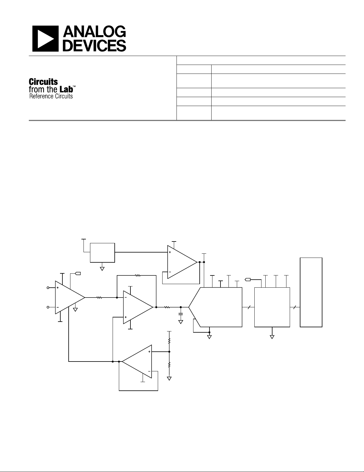
This circuit, shown in Figure 1, is a flexible sensor signal
conditioning block, with low noise, relatively high gain, and the
ability to dynamically change the gain in response to input level
changes without affecting performance, while still maintaining
a wide dynamic range. Existing sigma-delta technology can
each circuit, and their function a
suitability and applicability for your use and application. Accordingly, in no event shall Analog Dev ices
Figure 1. Wide Dynamic Range Signal Conditioning Circuit with Autoranging PGA and Oversampling SAR ADC (Note: All Connections and Decoupling Not Shown)
provide the dynamic range needed for many applications, but
only at the expense of low update rates. This circuit presents an
alternative approach that uses the AD7985 16-bit, 2.5 MSPS
PulSAR® successive-approximation ADC, combined with an
autoranging AD8253 iCMOS® programmable gain
instrumentation amplifier (PGA) front end. With gain that
changes automatically based on analog input value, it uses
oversampling and digital processing to increase the dynamic
range of the system to more than 125 dB.
One Technology Way, P.O. Box 9106, Norwood, MA 02062-9106, U.S.A.
Tel: 781.329.4700
www.analog.com

CN-0260 Circuit Note
OSR
F
SIGNAL
FS (MCLK)
ANALOG
ANTIALIAS
OSR INCREASED
F
SIGNAL
FS (MCLK)
ANALOG
ANTIALIAS
10451-002
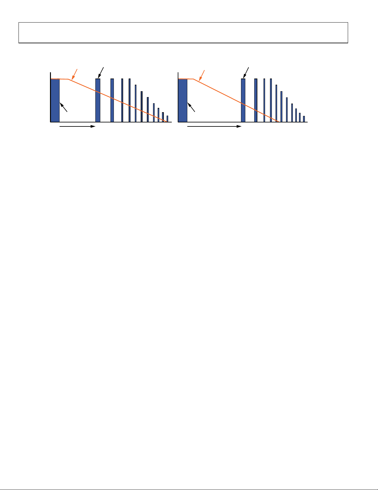
Figure 2. Increasing Oversampling Ratio (OSR) Reduces Noise
CIRCUIT DESCRIPTION
There are many applications that require wide dynamic range.
Weigh scale systems typically use load cell bridge sensors with
maximum full-scale outputs of 1 mV to 2 mV. Such systems
may require resolutions on the order of 1,000,000 to 1, which,
when referred to a 2 mV full-scale input, call for a high
performance, low noise, high gain amplifier and a sigma-delta
modulator. Similarly, chemical and blood analyses for medical
applications often use photodiode sensors, producing very
small currents that need to be accurately measured. Some
applications, such as vibration monitoring systems, contain
both ac and dc information, so the ability to accurately monitor
both small and large signals is growing in importance. Sigmadelta ADCs implement this well in many cases but are limited
when both ac and dc measurements are needed and fast gain
switching is required.
Oversampling is the process of sampling the input signal at a
much higher rate than the Nyquist frequency. As a general rule,
every doubling of the sampling frequency yields approximately
a 3 dB improvement in noise performance within the original
signal bandwidth. The oversampling ADC is followed by digital
postprocessing to remove the noise outside the signal
bandwidth, as shown in Figure 2.
To achieve maximum dynamic range, a front-end PGA stage
can be added to increase the effective signal-to-noise ratio
(SNR) for very small signal inputs. Consider a system dynamic
range requirement of >126 dB. First, calculate the minimum
rms noise required to achieve this dynamic range. For example,
a 3 V input range (6 V p-p) has a 2.12 V full-scale rms value
(6/2√2). The maximum allowable system noise is calculated as
126 dB = 20 log (2.12 V/rms noise)
Thus, the rms noise ≈ 1 μV rms.
Now, consider the system update rate, which will determine the
oversampling ratio and the maximum amount of noise, referred
to the input (RTI), that can be tolerated in the system. For
example, with the AD7985 16-bit, 2.5 MSPS PulSAR ADC
Rev. 0 | Page 2 of 6
running at 600 kSPS (11 mW dissipation) and an oversampling
ratio of 72, the effective throughput rate of the system after
averaging and decimation is 600 kSPS ÷ 72 = 8.33 kSPS.
The input signal is therefore limited to a bandwidth of
approximately 4 kHz.
The total rms noise is simply the noise density (ND) times √f,
so the maximum allowable input spectral noise density (ND)
can be calculated as
1 μV rms = ND × √4 kHz
Or, ND = 15.8 nV/√Hz.
From this figure of merit for RTI system input noise, a suitable
instrumentation amplifier can be chosen that will provide
sufficient analog front-end gain (when summed with the SNR
of the ADC, with associated oversampling) to achieve the
required 126 dB. For the AD7985, the typical SNR figure is
89 dB, and oversampling by 72 yields another ~18 dB
improvement (72 is approximately 2
6
, and each doubling adds
3 dB). Achieving 126 dB DR still requires more than 20 dB
improvement, which can come from the gain provided by the
analog PGA stage. The instrumentation amplifier must provide
a gain of ≥20 (or whatever will not exceed a noise density
specification of 15.8 nV/√Hz).
A system-level solution to implement front-end PGA gain and
ADC oversampling as discussed above is shown in Figure 1.
The input stage uses the AD8253 very low noise 10 nV/√Hz
digitally controlled instrumentation amplifier. Gain options are
the following: G = 1, 10, 100, 1000.
The AD8021 is a 2.1 nV/√Hz low noise, high speed amplifier
capable of driving the AD7985. It also level shifts and attenuates
the AD8253 output. Both the AD8253 and AD8021 are operated
with an external common-mode bias voltage of 2.25 V, which
combine to maintain the same common-mode voltage on the
input to the ADC. With a 4.5 V reference, the input range of the
ADC is 0 V to 4.5 V.
 Loading...