Circuit Note
Circuit Designs Using Analog Devices Products
Apply these product pairings quickly and with confidence.
For more information and/or support call 1-800-AnalogD
(1-800-262-5643) or visit www.analog.com/CN0259.
Devices Connected/Referenced
AD6657A Quad IF Receiver, 200 MSPS Sampling Rate
ADL5565
6.0 GHz Ultrahigh Dynamic Range
Differential Amplifier
High Performance 65 MHz Bandwidth Quad IF Receiver with Antialiasing Filter
and 184.32 MSPS Sampling Rate
EVALUATION AND DESIGN SUPPORT
Design and Integration Files
Schematics, Layout Files, Bill of Materials
CIRCUIT FUNCTION AND BENEFITS
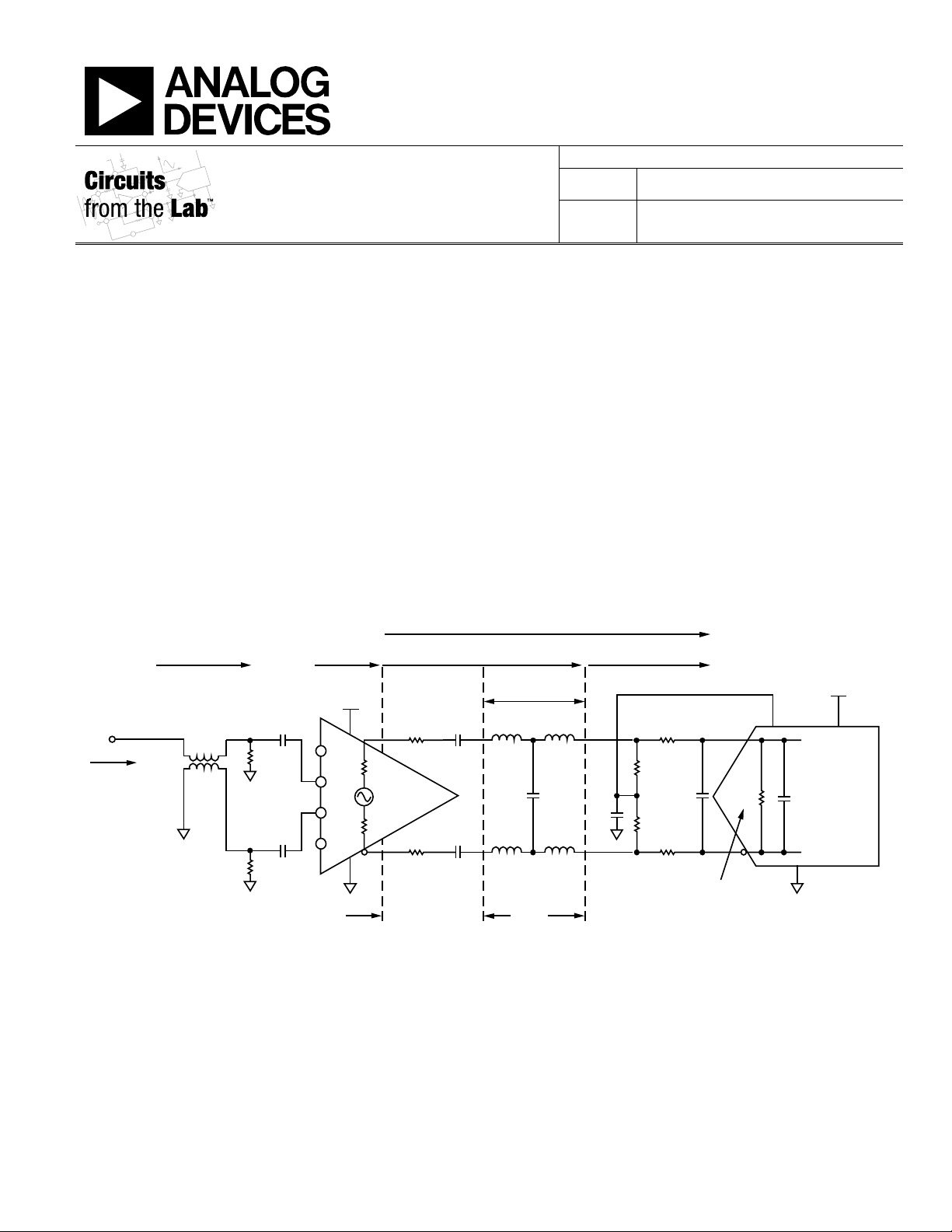
The circuit, shown in Figure 1, is a 65 MHz bandwidth receiver
front end based on the ADL5565 ultrahigh dynamic range
differential amplifier driver and the 11-bit, 200 MSPS
AD6657A quad IF receiver.
The fourth-order Butterworth antialiasing filter is optimized based
on the performance and interface requirements of the amplifier
and IF receiver. The total insertion loss due the filter network
and other resistive components is only 2.0 dB. The overall circuit
has a bandwidth of 65 MHz, with the low-pass filter having a
1 dB bandwidth of 190 MHz and a 3 dB bandwidth of 210 MHz.
The pass-band flatness is 1 dB.
The circuit is optimized to process a 65 MHz bandwidth IF signal
centered at 140 MHz with a sampling rate of 184.32 MSPS. The
SNR and SFDR measured with a 140 MHz analog input across
the 65 MHz band are 70.1 dBFS and 80.9 dBc, respectively.
2.0dB LOSS
CN-0259
0.1dB LO SS
ANALOG
INPUT
+4.9dBm
AT 10MHz
INPUT
Z = 50Ω
OVERALL GAIN = 3.9dB
ECT 1-1-13M
XFMR
1:1 Z
40Ω
40Ω
0.1µF
Z
= 200Ω
I
0.1µF
6dB GAIN
+3.3V
VIP2
VIP1
VIN1
VIN2
5Ω
ADL5565
G= 6dB
5Ω
1.875dB LO SS 0.125dB LO SS
FILTER
R
A
20Ω
R
20Ω
0.1µF
A
0.1µF
72nH
72nH
110nH
7.5pF
110nH
209Ω50Ω249Ω
0.1µF
110Ω
R
TADC
110Ω
R
TADC
R
15Ω
R
15Ω
KB
1.5pF
KB
R
ADC
2.4kΩ
FS 1.75V p-p DIFF
VCM
2.2pF
INTERNAL
INPUT Z
+1.8V
AD6657A
11-BIT
200MSPS
IF RECEIVER
10443-001
Figure 1. Single Channel of Quad IF Receiver Front End (Simplified Schematic: All Connections and Decoupling Not Shown)
Gains, Losses, and Signal Levels Measured Values at 10 MHz
Rev. A
Circuits from the Lab™ circuits from Analog Devices have been designed and built by Analog Devices
engineers. Standard engineering practices have been employed in the design and construction of
each circuit, and their function and performance have been tested and verified in a lab environment at
room temperature. However, you are solely responsible for testing the circuit and determining its
suitability and applicability for your use and application. Accordingly, in no event shall Analog Devices
be liable for direct, indirect, special, incidental, consequential or punitive damages due to any cause
whatsoever connected to the use of any Circuits from the Lab circuits. (Continued on last page)
One Technology Way, P.O. Box 9106, Norwood, MA 02062-9106, U.S.A.
Tel: 781.329.4700 www.analog.com
Fax: 781.461.3113 ©2012 Analog Devices, Inc. All rights reserved.

CN-0259 Circuit Note
H
H
H
H
CIRCUIT DESCRIPTION
The circuit shown in Figure 1 accepts a single-ended input
and converts it to differential using a wide bandwidth (3 GHz)
M/A-COM ECT1-1-13M 1:1 transformer. The ADL5565 6.0 GHz
differential amplifier has a differential input impedance of 200 Ω
when operating at a gain of 6 dB, 100 Ω when operating at a
gain of 12 dB, and 67 Ω when operating at a gain of 15.5 dB.
The ADL5565 is an ideal driver for the AD6657A, and the fully
differential architecture through the low-pass filter and into the
ADC provides good high frequency common-mode rejection,
as well as minimizes second-order distortion products. The
ADL5565 provides a gain of 6 dB, 12 dB, or 15.5 dB depending
on the input connection. In the circuit, a gain of 6 dB was used
to compensate for the insertion loss of the filter network and
the transformer (approximately 2.1 dB), providing an overall
signal gain of 4.0 dB. The gain also helps minimize noise
impacts from the amplifier.
The AD6657A is a quad IF receiver where each ADC output is
connected internally to a digital noise shaping requantizer (NSR)
block. The integrated NSR circuitry allows for improved SNR
performance in a smaller frequency band within the Nyquist
bandwidth.
The NSR block can be programmed to provide a bandwidth of
either 22%, 33%, or 36% of the sampling rate. For the data taken
in this circuit note, the sampling rate was 184.32 MSPS, and the
following NSR settings applied:
• NSR bandwidth = 36%
• Tuning word (TW) = 12
• Left band edge = 11.06 MHz (input = 173.26 MHz)
• Center frequency = 44.24 MHz (input = 140.08 MHz)
• Right band edge = 77.41 MHz (input = 106.91 MHz)
Details of the operation of the NSR blocks can be found in the
AD6657A data sheet.
The antialiasing filter is a fourth-order Butterworth low-pass
filter designed with a standard filter design program (Agilent ADS
in this case). A Butterworth filter was chosen because of its flat
response. A fourth-order filter yields an ac noise bandwidth
ratio of 1.03. Other filter design programs are available from
Nuhertz Technologies or Quite Universal Circuit Simulator
(Qucs) Simulation.
To achieve best performance, load the ADL5565 with a net
differential load of at least 200 Ω. The 20 Ω series resistors
isolate the filter capacitance from the amplifier output and,
when added with the downstream impedance, yields a net load
impedance of 249 Ω.
The 15 Ω resistors in series with the ADC inputs isolate internal
switching transients from the filter and the amplifier. The 110 Ω
resistors in parallel with the ADC serve to reduce the input
impedance of the ADC for more predictable performance.
The differential input impedance of the AD6657A is
approximately 2.4 kΩ in parallel with 2.2 pF. The real and
imaginary components are a function of input frequency for
this type of switched capacitor input ADC; the analysis can be
found in Application Note AN-742.
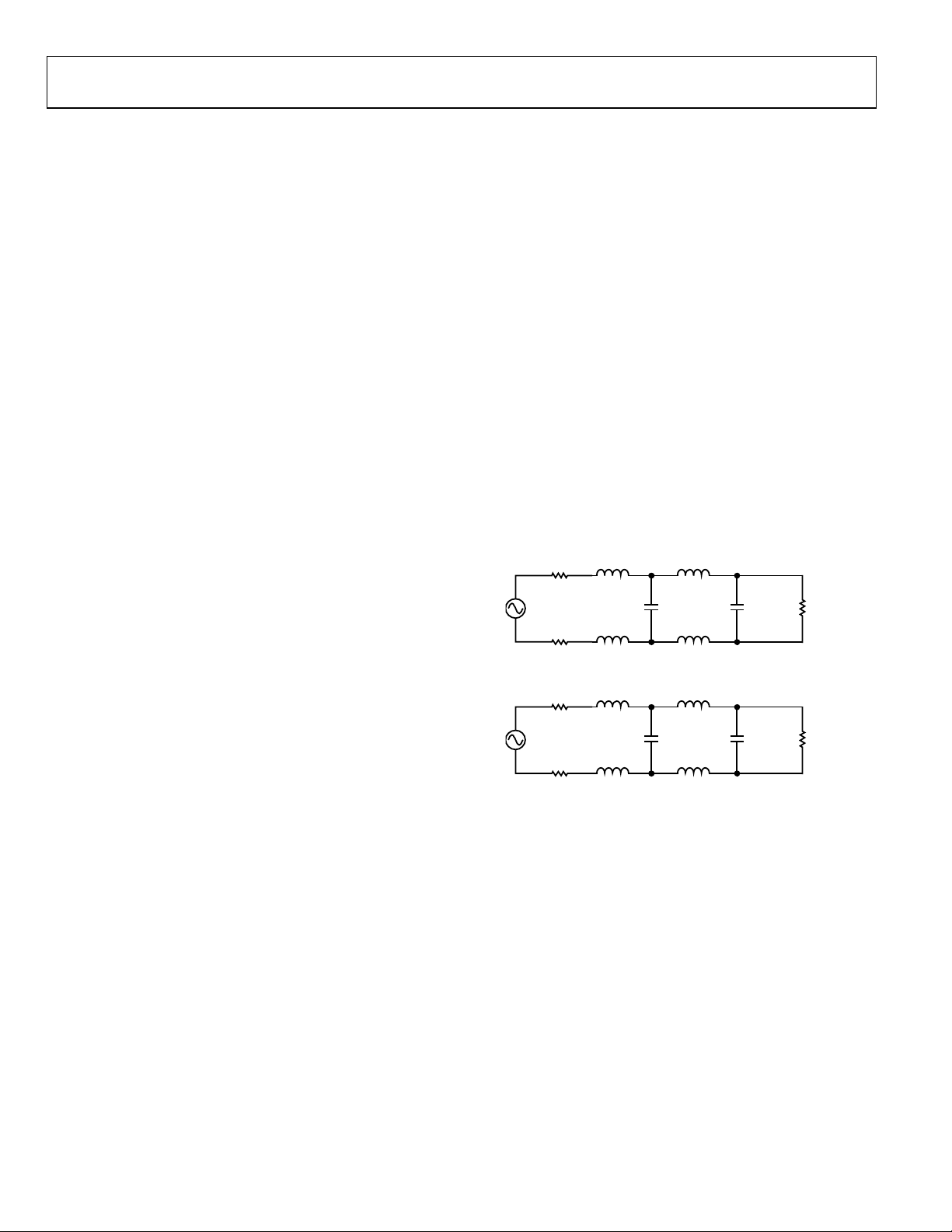
The fourth-order Butterworth filter was designed with a source
impedance of 50 Ω, a load impedance of 209 Ω, and a 3 dB
bandwidth of 190 MHz. The final circuit values for the filter are
shown in Figure 3. The values generated from the filter program
are shown in Figure 2. The values chosen for the filter passive
components were the closest standard values to those generated
by the program. The internal 2.2 pF capacitance of the ADC was
utilized as the final shunt capacitance in the filter design. A small
amount of additional shunt capacitance (1.5 pF) was added into
the final shunt capacitance at the ADC inputs to help reduce kick
back charge currents from the ADC input sampling network
and to optimize the filter performance.
As seen with this design, obtaining the optimal performance
can sometimes be an iterative process. The filter program design
values were quite close to the final values, but due to some board
parasitics, the final values of the filter were slightly different.
Figure 3 shows the final design values for the filter.
110n
25Ω
110nH
25Ω
Figure 2. Filter Program Initial Design for Fourth-Order Differential
Butterworth Filter with Z
25Ω
25Ω
Figure 3. Final Design Values for Fourth-Order Differential Butterworth Filter
72n
72nH
with Z
= 50 Ω, ZL = 209 Ω, FC = 190 MHz
S
82n
6.0pF 2.2pF
82nH
= 50 Ω, ZL = 209 Ω, FC = 190 MHz
S
110n
7.5pF 3.7pF
110nH
209Ω
209Ω
10443-002
10443-003
The measured performance of the system is summarized in
Tabl e 1 , where the 3 dB bandwidth is 210 MHz. The total
insertion loss of the network is approximately 2 dB. The
bandwidth response of the final filter circuit is shown in
Figure 4, and the SNR, SFDR performance in Figure 5.
Rev. A | Page 2 of 5
 Loading...