Circuits from the Lab™ circuits from Analog Devices have been designed and built by Analog Devices
each circuit, and their function and performance have been tested and verified in a lab environment at
suitability and applicability for your use and application. Accordingly, in no event shall Analog Devices
be liable for direct, indirect, special, incidental, consequential or punitive damages due to any cause
EXTERNAL
FREQUENCY
REFERENCE
INPUT
DUAL MODULUS P LL
WITH O N CHIP VCO
EXTERNAL LOOP
FILTER
EXTERNAL LOOP
FILTER
AD9516
AD9122
ADRF6702
PLL REF E RE NCE
INPUT
PROGRAMMABLE DIVI DE R
PROGRAMMABLE DIVI DE R
OPTIONAL
EXTERNAL
2 × LO (I/O)
INTERNALLY
GENERATED
2 × LO
ADRF6702
RF OUTPUT
AD9122 DAC
SAMPLE CLOCK
IDAC
I CHANNEL PASS IVE INT E RFACE FILTER
QDAC
Q CHANNEL PASS IVE INT E RFACE FILTER
16-BIT
DATA BUS
(I)
16-BIT
DATA BUS
(Q)
32-BIT NCO
2×/4×/8×
INTERPOLATION
FILTERS
2×/4×/8×
INTERPOLATION
FILTERS
INTERNAL LO
SYNTHESIZER/PLL
INTERNAL
VCO
10165-001
÷2
MODULATOR
CORE
PLL CORE ( P FD, CHARGE
PUMP, DIVIDER)
Circuit Note
CN-0243
Devices Connected/Referenced
Circuits from the Lab™ reference circuits are
engineered and tested for quick and easy
ADRF6702
system integration to help solve today’s analog,
mixed-signal, and RF design challenges.
For more information and/or support, visit
www.analog.com/CN0243.
AD9122 Dual, 16-Bit, 1230 MSPS, TxDAC®
AD9516-0/AD9516-1/
AD9516-2/AD9516-3/
AD9516-4
High Dynamic Range RF Transmitter Signal Chain Using Single External Frequency
1200 MHz to 2400 MHz Quadrature
Modulator with1550 MHz to 2150 MHz
Fractional-N PLL and Integrated VCO
Clock Generator with Integrated VCO
with Various Frequency Range Options
from 1.45 GHz to 2.95 GHz
Reference for DAC Sample Clock and IQ Modulator LO Generation
EVALUATION AND DESIGN SUPPORT
Circuit Evaluation Boards
CN-0243 Circuit Evaluation Board (EVAL-CN0243-EB1Z)
Design and Integration Files
Schematics, Layout Files, Bill of Materials
CIRCUIT FUNCTION AND BENEFITS
The combination of the ADRF6702 IQ modulator and the
AD9122 16-bit dual 1.2 GSPS TxDAC has the dynamic range
necessary for a modern high level QAM or OFDM based
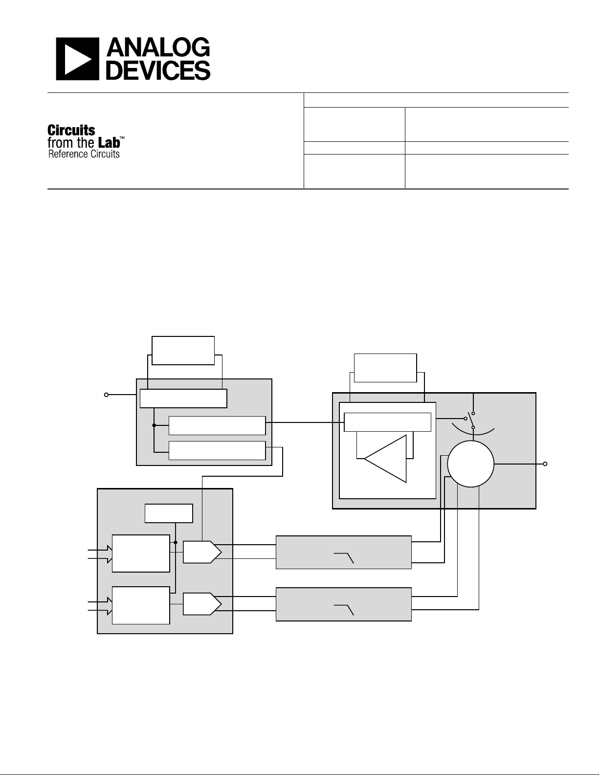
wireless transmitter as shown in Figure 1. The dynamic range
Rev.0
engineers. Standard engineering practices have been employed in the design and construction of
room temperature. However, you are solely responsible for testing the circuit and determining its
whatsoever connected to the use of any Circuits from the Lab circuits. (Continued on last page)
Figure 1. AD9122, ADRF6702, and AD9516 Used in a High Dynamic Range Transmitter
One Technology Way, P.O. Box 9106, Norwood, MA 02062-9106, U.S.A.
Tel: 781.329.4700
Fax: 781.461.3113 ©2011 Analog Devices, Inc. All rights reserved.
www.analog.com

CN-0243 Circuit Note
1065-002
–4x
–245.76 –184.32 –122.88 –61.44 61.44 122.88 184.32 245.76DC
FREQUENCY
FREQUENCY (x-FDATA)
0dB
–20dB
–40dB
–60dB
–80dB
–100dB
–3x –2x –1x DC 1x 2x 3x 4x
AMPLITUDE (dBFS)
of this circuit is good enough to enable both ZIF (zero IF/
baseband) and CIF (complex IF up to 200 MHz to 300 MHz).
The AD9122 has the option of up to 8× interpolation, as well as
a 32-bit NCO for very fine IF frequency selectivity.
Overall performance of a transmitter is highly dependent on the
dynamic range of the components directly in the signal chain.
In a mixed-signal transmitter using a DAC and IQ modulator,
the noise floor and distortion characteristics of these
components define the overall dynamic range of the signal
chain. However, the noise floor of the DAC can also be
degraded by sample clock jitter, and the IQ modulator
performance is dependent on the noise and spur characteristics
of its local oscillator (LO). Using high performance components
for sample clock and LO generation is, therefore, key to a high
performance transmitter.
In addition, generating these signals physically close to the DAC
and modulator on the PCB and using a single external reference
can make the design much simpler. Generating the sample
clock and LO (LO is very often a multi-GHz signal) separately
and at some distance from the DAC and IQ modulator requires
great care in the PCB layout. Subtle layout errors can cause
coupling to and from these critical signals and degrade overall
signal chain performance.
The signal chain performance is also heavily dependent on the
DAC/ IQ modulator interface filter. For optimal performance,
this passive filter should be designed after careful analysis of the
required system specifications.
The ADRF6702 includes an on-board fractional PLL for LO
generation so that a low frequency reference (typically less than
100 MHz) is all that is necessary to synthesize the IQ modulator
LO. Using the PLL in the AD9516 clock generator allows a
single reference to generate both the DAC sample clock and the
PLL reference for the ADRF6702.
The circuit in Figure 1 was built using the AD9516-0, but other
members of the AD9516 family could be used depending on the
desired internal VCO frequency.
CIRCUIT DESCRIPTION
ADRF6702 IQ Modulator with Internal LO Synthesizer,
Synthesizer IQ Modulator Interface
The ADRF6702 IQ modulator is a unique device in several
respects. In addition to its exceptional dynamic range, it also
includes a fractional-N PLL, which allows programming of
discrete LO frequency steps of less than 25 kHz while at the
same time keeping the overall frequency multiplication small
enough to avoid a large increase in phase noise from the
reference to the synthesizer output.
Another aspect of the ADRF6702 is the divide-by-2 architecture
of the IQ modulator. Traditional IQ modulators accept an LO
input frequency at 1× the desired LO. Internally, a distributed
RC network creates the desired in-phase and quadrature LO
signals from the single LO frequency input. Because this is a
passive RC network, the bandwidth over which quadrature
modulation accuracy is achieved is limited. Also, for good
quadrature accuracy, the external LO should be spectrally pure.
Harmonics on the LO with this traditional IQ modulator
architecture can degrade the overall modulation accuracy. For
this reason, when using a PLL synthesizer to generate an LO
signal for an IQ modulator, a sharp band-pass or low-pass filter
is often required at the IQ modulator LO input.
In the divide-by-2 LO architecture of the ADRF6702, a simple
digital divider is used internally to create nearly perfect
quadrature over a wide band. The PLL synthesizer generates the
2× LO internally, so that it does not have to be distributed
around the PCB, and no filter is required between the
synthesizer and IQ modulator LO because the 2× LO
architecture is only sensitive to the edges of the LO signal, not
the frequency content. For a detailed descripton of the effects of
LO harmonics on a 1× IQ modulator and the design of the LO
filter, see Circuit Note CN-0134.
Sampled Signal to RF, Overall Spur Floor
A baseband signal goes through a number of steps on the way to
the RF transmit frequency. The signal begins in the discrete
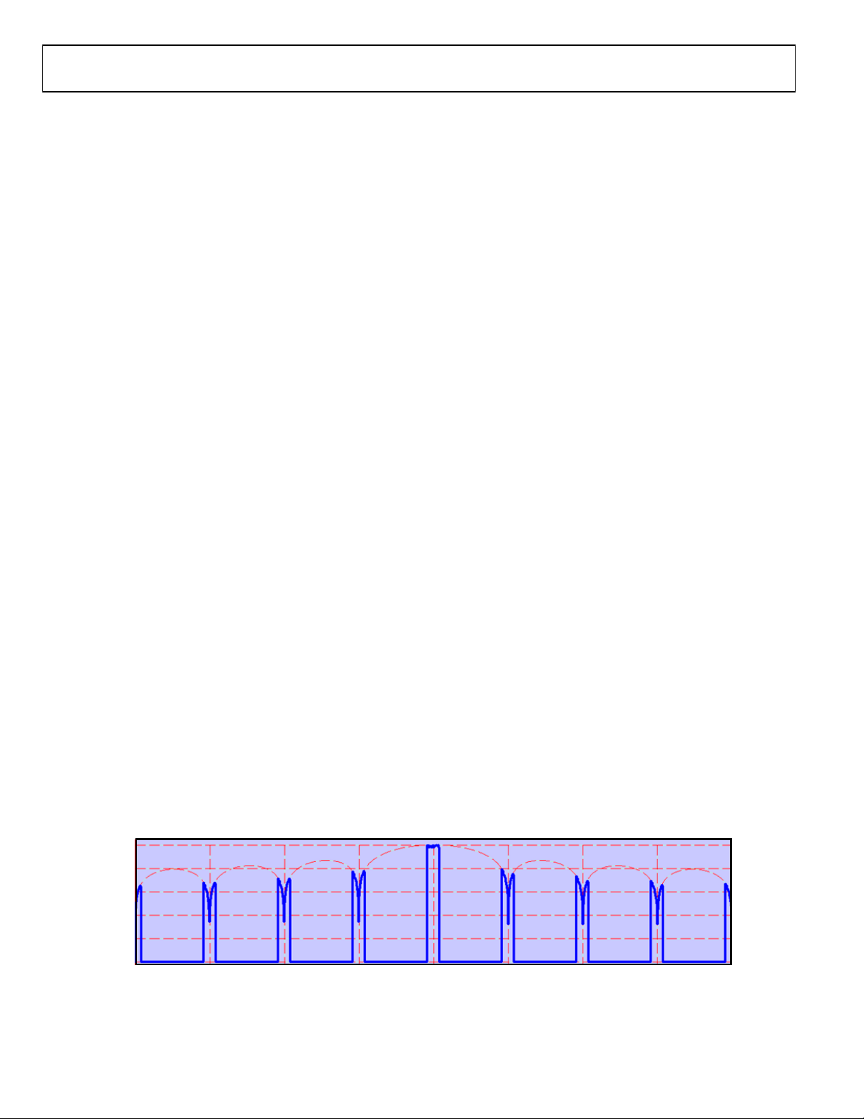
Figure 2. DAC Output Spectrum, Solid Blue Line Represents Baseband Signal and Images, Dotted Red Line Represents DAC Sinc Function
Rev. 0 | Page 2 of 8

Circuit Note CN-0243
1065-003
–4x
–245.76 –184.32 –122.88 –61.44 61.44 122.88 184.32 245.76DC
FREQUENCY
FREQUENCY (x-FDATA)
0dB
–20dB
–40dB
–60dB
–80dB
–100dB
–3x –2x –1x DC 1x 2x 3x 4x
AMPLITUDE (dBFS)
10165-004
Figure 3. DAC Output Spectrum Using 4× Interpolation, the Thin Blue Line Represents the DAC Interpolation Transfer Function
(sampled) domain and is synthesized by the DAC into the
analog domain. The results of this step are images and
distortion products generated by the DAC. As shown in Figure 2,
an ideal DAC with no distortion will generate images of a
baseband signal that must be filtered before being modulated.
The use of interpolation filters such as those in the AD9122 can
suppress most of the image energy, but an analog interface filter
between DAC and modulator will still be necessary. There is a
trade-off, however, between the order of the DAC interpolation
and the order of the analog filter. Higher DAC interpolation
rates mean lower required analog filter order and vice versa.
Figure 3 shows what the DAC output spectrum looks like when
using 4× interpolation, as an example.
A Multitude of Spurious Components at RF
The signal chain can add significant spurious components to the
spectrum, due both to modulation products, distortion
products, and integer multiples of the LO frequency. It we take
into account all of the possibilities for spurious which we have
discussed, the spurious content can consist of
(j × LO_freq) + (k × DAC_sample_rate) +
(l × DAC_NCO_freq) + (m × DAC_input_IF)
Where j, k, l, and m are integers over the range of negative
infinity to positive infinity.
and load impedances, as well as parasitics in the signal
traces, may add unwanted ripple in the filter pass band.
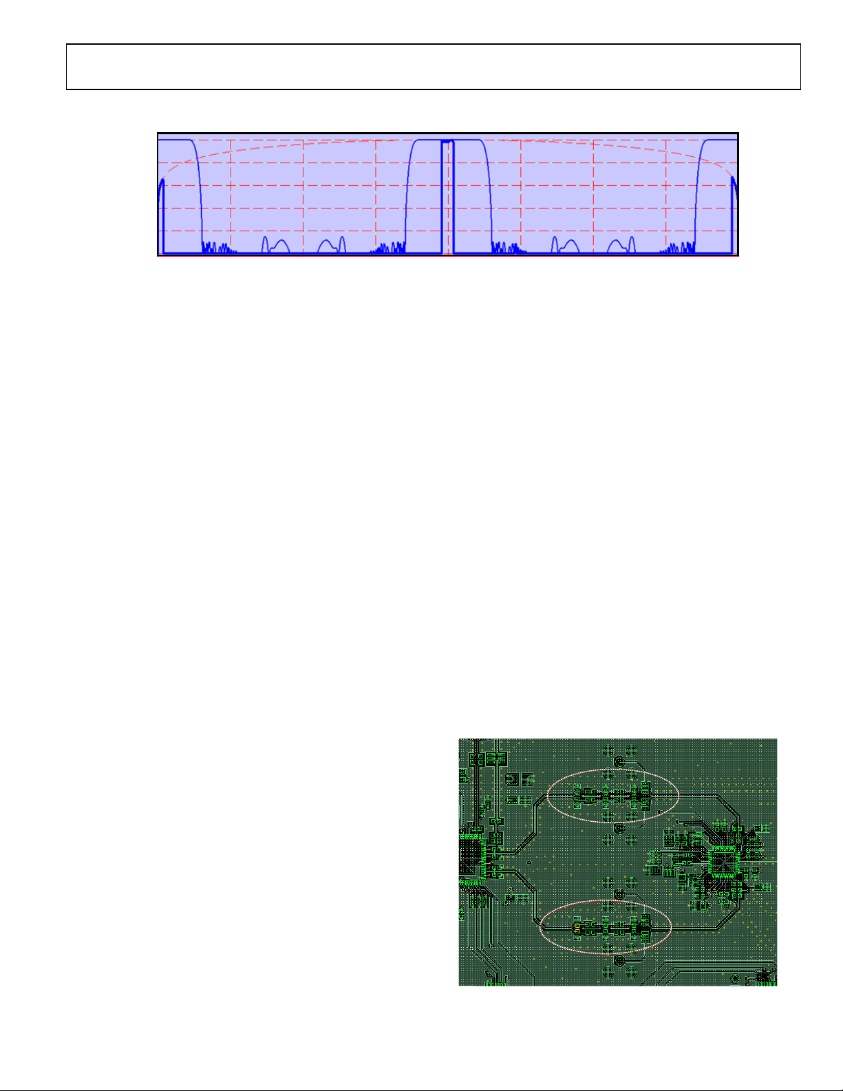
3. PCB layout. As shown in Figure 4, the I and Q
baseband inputs on the ADRF6702 IQ modulator are
located on opposite edges of the device. Note the filter
layout area within the dotted circles. To route the DAC
output signals to these pins, the traces must travel up
and then back down to get to the baseband pins on the
ADRF6702. These differential signal traces should be
of equal length, and any changes in direction of the
trace should be done by using 45° bends. If these
recommendations are not implemented, in-band
ripple, phase, or amplitude response may be degraded
in the filter response. Note that with this filter
topology, the capacitors can be used differentially
(across the signal path) or they can be used in a
common-mode connection by placing the filter caps
from the signal path pads to ground pads. There are
conditions (discussed later in this circuit note) where
common-mode capacitors improve performance vs.
differential-mode capacitors.
DAC/Modulator Passive Interface Filter
The key to reducing the overall spurious spectrum is the analog
interface filter between the DAC and the IQ modulator. The
design of the interface filter between the DAC and IQ modulator
must take into account multiple aspects of performance:
1. Filter topology, order, and 3 dB cutoff frequency
2. At dc, the DAC sees a load impedance equal to the
DAC termination resistors (typically a 100 Ω
differential impedance) in parallel with the input
impedance of the IQ modulator. The IQ modulator
impedance is often >1kΩ, so a shunt resistor is often
used across the IQ modulator inputs to create a similar
load impedance to the source. Unequal filter source
Rev. 0 | Page 3 of 8
Figure 4. PCB Layout for Transmitter, DAC/Mod Interface Filter Section
