Analog Devices AD9226 Datasheet
Complete 12-Bit, 65 MSPS
a
FEATURES
Signal-to-Noise Ratio: 69 dB @ f
Spurious-Free Dynamic Range: 85 dB @ f
Intermodulation Distortion of –75 dBFS @ f
ENOB = 11.1 @ f
= 10 MHz
IN
Low-Power Dissipation: 475 mW
No Missing Codes Guaranteed
Differential Nonlinearity Error: ⴞ0.6 LSB
Integral Nonlinearity Error: ⴞ0.6 LSB
Clock Duty Cycle Stabilizer
Patented On-Chip Sample-and-Hold with
Full Power Bandwidth of 750 MHz
Straight Binary or Two’s Complement Output Data
28-Lead SSOP, 48-Lead LQFP
Single 5 V Analog Supply, 3 V/5 V Driver Supply
Pin-Compatible to AD9220, AD9221, AD9223,
AD9224, AD9225
PRODUCT DESCRIPTION
The AD9226 is a monolithic, single-supply, 12-bit, 65 MSPS
analog-to-digital converter with an on-chip, high-performance
sample-and-hold amplifier and voltage reference. The AD9226
uses a multistage differential pipelined architecture with a patented input stage and output error correction logic to provide
12-bit accuracy at 65 MSPS data rates. There are no missing
codes over the full operating temperature range (guaranteed).
The input of the AD9226 allows for easy interfacing to both
imaging and communications systems. With a truly differential
input structure, the user can select a variety of input ranges and
offsets including single-ended applications.
The sample-and-hold amplifier (SHA) is well suited for IF
undersampling schemes such as in single-channel communication applications with input frequencies up to and well
beyond Nyquist frequencies.
The AD9226 has an on-board programmable reference. For system design flexibility, an external reference can also be chosen.
A single clock input is used to control all internal conversion
cycles. An out-of-range signal indicates an overflow condition
that can be used with the most significant bit to determine low
or high overflow.
= 31 MHz
IN
= 31 MHz
IN
= 140 MHz
IN
ADC Converter
AD9226
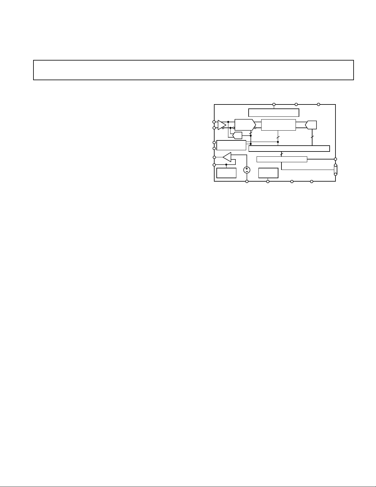
FUNCTIONAL BLOCK DIAGRAM
A/D
AD9226
DRVSS
DRVDD
3
OTR
BIT 1
(MSB)
BIT 12
(LSB)
AVDD
16
12
AVSS
VINA
VINB
CAPT
CAPB
VREF
SENSE
SHA
CALIBRATION
SELECT
REF
MDAC1
A/D
ROM
1V
REFCOM
CLK
DUTY CYCLE STABILIZER
8-STAGE
1-1/2-BIT PIPELINE
4
CORRECTION LOGIC
OUTPUT BUFFERS
MODE
SELECT
MODE
The AD9226 has two important mode functions. One will set
the data format to binary or two’s complement. The second will
make the ADC immune to clock duty cycle variations.
PRODUCT HIGHLIGHTS
IF Sampling—The patented SHA input can be configured for
either single-ended or differential inputs. It will maintain outstanding AC performance up to input frequencies of 300 MHz.
Low Power—The AD9226 at 475 mW consumes a fraction of
the power presently available in existing, high-speed monolithic
solutions.
Out of Range (OTR)—The OTR output bit indicates when
the input signal is beyond the AD9226’s input range.
Single Supply—The AD9226 uses a single 5 V power supply
simplifying system power supply design. It also features a separate digital output driver supply line to accommodate 3 V and
5 V logic families.
Pin Compatibility—The AD9226 is similar to the AD9220,
AD9221, AD9223, AD9224, and AD9225 ADCs.
Clock Duty Cycle Stabilizer—Makes conversion immune to
varying clock pulsewidths.
REV. 0
Information furnished by Analog Devices is believed to be accurate and
reliable. However, no responsibility is assumed by Analog Devices for its
use, nor for any infringements of patents or other rights of third parties
which may result from its use. No license is granted by implication or
otherwise under any patent or patent rights of Analog Devices.
One Technology Way, P.O. Box 9106, Norwood, MA 02062-9106, U.S.A.
Tel: 781/329-4700 World Wide Web Site: http://www.analog.com
Fax: 781/326-8703 © Analog Devices, Inc., 2000

AD9226–SPECIFICATIONS
(AVDD = 5 V, DRVDD = 3 V, f
DC SPECIFICATIONS
P
arameter Temp Test Level Min Typ Max Unit
RESOLUTION 12 Bits
ACCURACY
Integral Nonlinearity (INL) Full V ± 0.6 LSB
Differential Nonlinearity (DNL) Full V ± 0.6 LSB
No Missing Codes Guaranteed Full I 12 Bits
Zero Error Full V ± 0.3 % FSR
Gain Error 25°CI ± 2.0 % FSR
TEMPERATURE DRIFT
Zero Error Full V ± 2 ppm/°C
Gain Error
Gain Error
POWER SUPPLY REJECTION
AVDD (5 V ± 0.25 V) Full V ± 0.05 % FSR
INPUT REFERRED NOISE
VREF = 1.0 V Full V 0.5 LSB rms
VREF = 2.0 V Full V 0.25 LSB rms
ANALOG INPUT
Input Span (VREF = 1 V) Full V 1 V p-p
Input (VINA or VINB) Range Full IV 0 AVDD V
Input Capacitance Full V 7 pF
INTERNAL VOLTAGE REFERENCE
Output Voltage (1 V Mode) Full V 1.0 V
Output Voltage Tolerance (1 V Mode) 25°CI ± 15 mV
Output Voltage (2.0 V Mode) Full V 2.0 V
Output Voltage Tolerance (2.0 V Mode) 25°CI ± 29 mV
Output Current (Available for External Loads) Full V 1.0 mA
Load Regulation
REFERENCE INPUT RESISTANCE Full V 5 kΩ
POWER SUPPLIES
Supply Voltages
AVDD Full V 4.75 5 5.25 V (± 5% AVDD
DRVDD Full V 2.85 5.25 V (± 5% DRVDD
Supply Current
IAVDD
IDRVDD
POWER CONSUMPTION
NOTES
1
Includes internal voltage reference error.
2
Excludes internal voltage reference error.
3
Load regulation with 1 mA load current (in addition to that required by the AD9226).
4
AVDD = 5 V
5
DRVDD = 3 V
Specifications subject to change without notice.
1
2
(VREF = 2 V) Full V 2 V p-p
3
4
5
4, 5
noted.)
25°CI ± 1.6 LSB
25°CI ± 1.0 LSB
25°CI ± 1.4 % FSR
Full V ± 0.6 % FSR
Full V ± 26 ppm/°C
Full V ± 0.4 ppm/°C
25°CI ± 0.4 % FSR
Full V 0.7 mV
25°C I 1.5 mV
Full V 86 mA (2 V External VREF)
25°C I 90.5 mA (2 V External VREF)
Full V 14.6 mA (2 V External VREF)
25°C I 16.5 mA (2 V External VREF)
Full V 475
25°C I 500 mW (2 V External VREF)
= 65 MSPS, VREF = 2.0 V, Differential inputs, T
SAMPLE
MIN
to T
unless otherwise
MAX
Operating)
Operating)
–2–
REV. 0
AD9226
DIGITAL SPECIFICATIONS
(AVDD = 5 V, DRVDD = 3 V, f
= 65 MSPS, VREF = 2.0 V, T
SAMPLE
MIN
to T
, unless otherwise noted.)
MAX
Parameters Temp Test Level Min Typ Max Unit
LOGIC INPUTS (Clock, DFS
Output Enable
1
)
1
, Duty Cycle1, and
High-Level Input Voltage Full IV 2.4 V
Low-Level Input Voltage Full IV 0.8 V
High-Level Input Current (V
Low-Level Input Current (V
Input Capacitance Full V 5 pF
Output Enable
1
= AVDD) Full IV –10 +10 µA
IN
= 0 V) Full IV –10 +10 µA
IN
Full IV V
DRVDD
2
05– .
DRVDD
2
05+ .
LOGIC OUTPUTS (With DRVDD = 5 V)
High-Level Output Voltage (I
High-Level Output Voltage (I
Low-Level Output Voltage (I
Low-Level Output Voltage (I
= 50 µA) Full IV 4.5 V
OH
= 0.5 mA) Full IV 2.4 V
OH
= 1.6 mA) Full IV 0.4 V
OL
= 50 µA) Full IV 0.1 V
OL
Output Capacitance 5pF
LOGIC OUTPUTS (With DRVDD = 3 V)
High-Level Output Voltage (I
High-Level Output Voltage (I
Low-Level Output Voltage (I
= 50 µA) Full IV 2.95 V
OH
= 0.5 mA) Full IV 2.80 V
OH
= 1.6 mA) Full IV 0.4 V
OL
Low-Level Output Voltage (IOL = 50 µA) Full IV 0.05 V
NOTES
1
LQFP package.
Specifications subject to change without notice.
(T
to T
SWITCHING SPECIFICATIONS
MIN
with AVDD = 5 V, DRVDD = 3 V, CL = 20 pF)
MAX
Parameters Temp Test Level Min Typ Max Unit
Max Conversion Rate Full VI 65 MHz
Clock Period
CLOCK Pulsewidth High
CLOCK Pulsewidth Low
1
2
2
Full V 15.38 ns
Full V 3 ns
Full V 3 ns
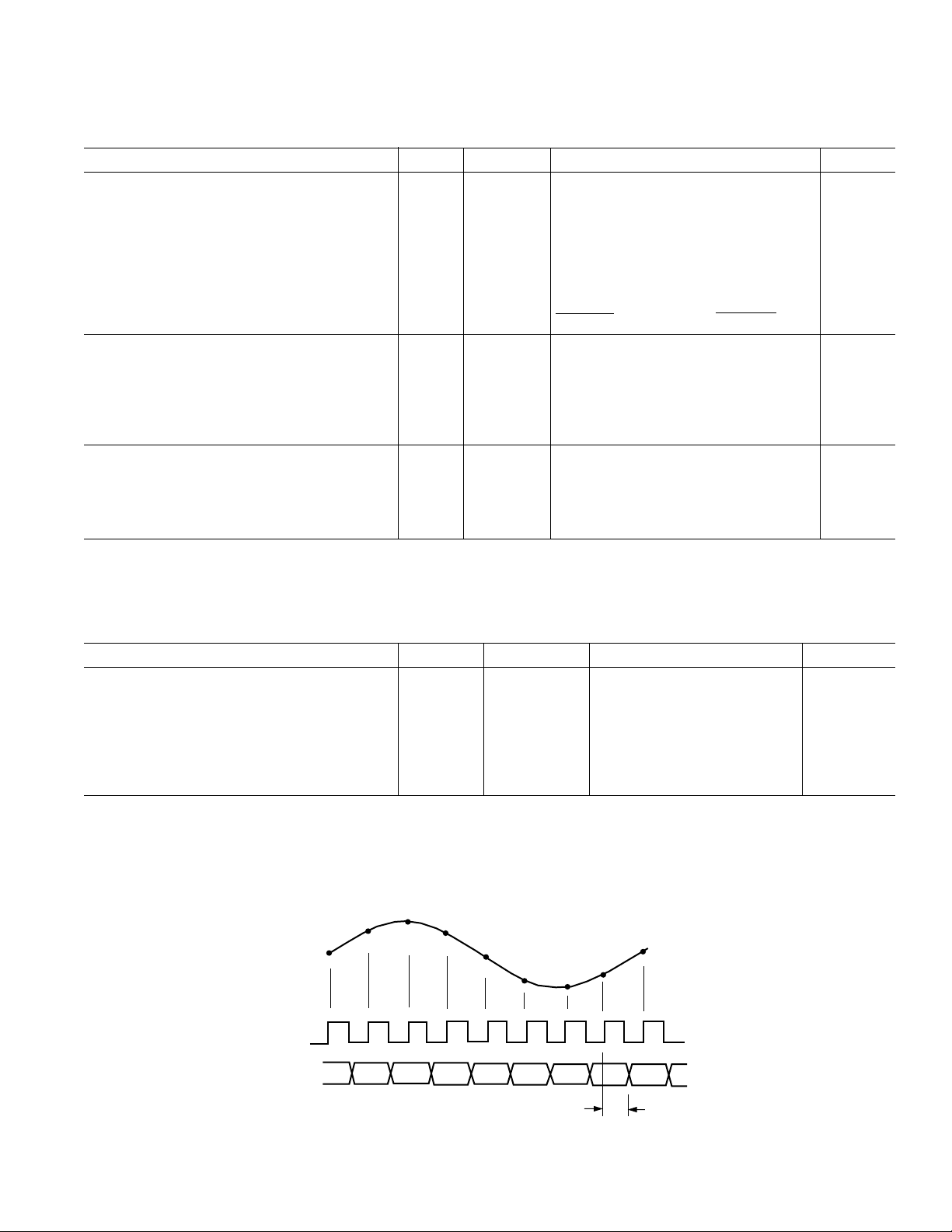
Output Delay Full V 3.5 7 ns
Pipeline Delay (Latency) Full V 7 Clock Cycles
Output Enable Delay
NOTES
1
The clock period may be extended to 10 µs without degradation in specified performance @ 25°C.
2
When MODE pin is tied to AVDD or grounded, the AD9226 SSOP is not affected by clock duty cycle.
3
LQFP package.
Specifications subject to change without notice.
3
n+1
ANALOG
INPUT
CLOCK
DATA
n
n–8 n–7 n–6 n–5 n–4 n–3
OUT
Full V 15 ns
n+2
n+3
n+7
n–1
n+8
n
n+1
n+4
n+5
n+6
n–2
REV. 0
Figure 1. Timing Diagram
–3–
TOD = 7.0 MAX
3.5 MIN

AD9226–SPECIFICATIONS
AC SPECIFICATIONS
(AVDD = 5 V, DRVDD = 3 V, f
= 65 MSPS, VREF = 2.0 V, T
SAMPLE
MIN
to T
, Differential Input unless otherwise noted.)
MAX
Parameter Temp Test Level Min Typ Max Unit
SIGNAL-TO-NOISE RATIO
fIN = 2.5 MHz Full V 68.9 dBc
25°C
= 15 MHz Full V 68.4 dBc
f
IN
25°C
f
= 31 MHz Full V 68 dBc
IN
= 60 MHz Full V 68 dBc
f
IN
fIN = 200 MHz
1
Full V 65 dBc
I 68 dBc
I 67.4 dBc
SIGNAL-TO-NOISE RATIO AND DISTORTION
fIN = 2.5 MHz Full V 68.8 dBc
25°C
= 15 MHz Full V 68.3 dBc
f
IN
25°C
= 31 MHz Full V 67 dBc
f
IN
= 60 MHz Full V 67 dBc
f
IN
fIN = 200 MHz
1
Full V 60 dBc
I 67.9 dBc
I 67.3 dBc
TOTAL HARMONIC DISTORTION
fIN = 2.5 MHz Full V –84 dBc
25°C
f
= 15 MHz Full V –82.3 dBc
IN
25°C
= 31 MHz Full V –68 dBc
f
IN
f
= 60 MHz Full V –68 dBc
IN
fIN = 200 MHz
1
Full V –61 dBc
I –77.0 dBc
I –76.0 dBc
SECOND AND THIRD HARMONIC DISTORTION
fIN = 2.5 MHz Full V –86.5 dBc
25°C
f
= 15 MHz Full V –86.7 dBc
IN
25°C
= 31 MHz Full V –83 dBc
f
IN
f
= 60 MHz Full V –82 dBc
IN
fIN = 200 MHz
1
Full V –75 dBc
I –78 dBc
I –76 dBc
SPURIOUS FREE DYNAMIC RANGE
fIN = 2.5 MHz Full V 86.4 dBc
25°C
f
= 15 MHz Full V 85.5 dBc
IN
25°C
= 31 MHz Full V 82 dBc
f
IN
f
= 60 MHz Full V 81 dBc
IN
fIN = 200 MHz
1
Full V 60 dBc
I 78 dBc
I 76 dBc
ANALOG INPUT BANDWIDTH 25°C V 750 MHz
NOTES
1
1.0 V Reference and Input Span
Specifications subject to change without notice.
–4–
REV. 0
AD9226
WARNING!
ESD SENSITIVE DEVICE
EXPLANATION OF TEST LEVELS
Test Level
I. 100% production tested.
II. 100% production tested at 25°C and sample tested at
specified temperatures. AC testing done on sample basis.
III. Sample tested only.
IV. Parameter is guaranteed by design and characterization
testing.
V. Parameter is a typical value only.
VI. All devices are 100% production tested at 25°C; sample tested
at temperature extremes.
ABSOLUTE MAXIMUM RATINGS
1
With
Pin Name Respect to Min Max Unit
AVDD AVSS –0.3 +6.5 V
DRVDD DRVSS –0.3 +6.5 V
AVSS DRVSS –0.3 +0.3 V
AVDD DRVDD –6.5 +6.5 V
REFCOM AVSS –0.3 +0.3 V
CLK, MODE AVSS –0.3 AVDD + 0.3 V
Digital Outputs DRVSS –0.3 DRVDD + 0.3 V
VINA, VINB AVSS –0.3 AVDD + 0.3 V
VREF AVSS –0.3 AVDD
SENSE AVSS –0.3 AVDD
CAPB, CAPT AVSS –0.3 AVDD
2
OEB
CM LEVEL
2
VR
DRVSS –0.3 DRVDD + 0.3 V
2
AVSS –0.3 AVDD + 0.3 V
AVSS –0.3 AVDD + 0.3 V
+ 0.3 V
+ 0.3 V
+ 0.3 V
Junction Temperature 150 °C
Storage Temperature –65 +150 °C
Lead Temperature (10 sec) 300 °C
NOTES
1
Stresses above those listed under Absolute Maximum Ratings may cause perma-
nent damage to the device. This is a stress rating only; functional operation of the
device at these or any other conditions above those indicated in the operational
sections of this specification is not implied. Exposure to absolute maximum ratings
for extended periods may affect device reliability.
2
LQFP package.
THERMAL RESISTANCE
θJC SSOP . . . . . . . . . . . . . . . . . . . . . . . . . . . . . . . . . . . 23°C/W
θ
SSOP . . . . . . . . . . . . . . . . . . . . . . . . . . . . . . . . . . 63.3°C/W
JA
LQFP . . . . . . . . . . . . . . . . . . . . . . . . . . . . . . . . . . . 17°C/W
θ
JC
θ
LQFP . . . . . . . . . . . . . . . . . . . . . . . . . . . . . . . . . .76.2°C/W
JA
ORDERING GUIDE
Model Temperature Range Package Description Package Option
AD9226ARS –40°C to +85°C 28-Lead Shrink Small Outline (SSOP) RS-28
AD9226AST –40°C to +85°C 48-Lead Thin Plastic Quad Flatpack (LQFP) ST-48
AD9226-EB Evaluation Board (SSOP)
AD9226-LQFP-EB Evaluation Board (LQFP)
CAUTION
ESD (electrostatic discharge) sensitive device. Electrostatic charges as high as 4000 V readily
accumulate on the human body and test equipment and can discharge without detection. Although
the AD9226 features proprietary ESD protection circuitry, permanent damage may occur on
devices subjected to high-energy electrostatic discharges. Therefore, proper ESD precautions are
recommended to avoid performance degradation or loss of functionality.
REV. 0
–5–
AD9226
AVSS
AVSS
AVDD
AVDD
NC
NC
CLK
NC
OEB
NC
NC
(LSB) BIT 12
NC = NO CONNECT
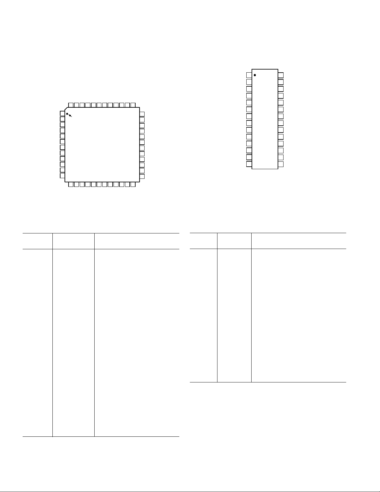
48-PIN FUNCTION DESCRIPTIONS
PIN CONNECTION
48-Lead LQFP
VR
VINB
VINA
CM LEVELNCMODE1
CAPT
AD9226
BIT 9
BIT 8
BIT 7
CAPT
BIT 6
48 47 46 45 44 39 38 3743 42 41 40
1
PIN 1
2
IDENTIFIER
3
4
5
6
7
8
9
10
11
12
13 14 15 16 17 18 19 20 21 22 23 24
BIT 11
DRVSS
DRVDD
TOP VIEW
(Not to Scale)
BIT 10
CAPB
CAPB
REF COM (AVSS)
BIT 5
DRVSS
DRVDD
VREF
BIT 4
36
SENSE
35
MODE2
34
AVDD
33
AVSS
32
AVSS
31
AVDD
30
DRVSS
29
DRVDD
28
OTR
BIT 1 (MSB)
27
BIT 2
26
BIT 3
25
PIN CONNECTION
28-Lead SSOP
CLK
(LSB) BIT 12
BIT 11
BIT 10
BIT 9
BIT 8
BIT 7
BIT 6
BIT 5
BIT 4
BIT 3
BIT 2
(MSB) BIT 1
OTR
1
2
3
4
5
6
AD9226
7
TOP VIEW
(Not to Scale)
8
9
10
11
12
13
14
28
DRVDD
27
DRVSS
26
AVDD
25
AVSS
24
VINB
23
VINA
22
MODE
21
CAPT
20
CAPB
19
REFCOM (AVSS)
18
VREF
17
SENSE
16
AVSS
15
AVDD
28-PIN FUNCTION DESCRIPTIONS
Pin
Number Name Description
1, 2, 32, 33 AVSS Analog Ground
3, 4, 31, 34 AVDD 5 V Analog Supply
5, 6, 8, 10, NC No Connect
11, 44
7 CLK Clock Input Pin
9 OEB Output Enable (Active Low)
12 BIT 12 Least Significant Data Bit (LSB)
13 BIT 11 Data Output Bit
14, 22, 30 DRVSS Digital Output Driver Ground
15, 23, 29 DRVDD 3 V to 5 V Digital Output
Driver Supply
16–21, BITS 10–5, Data Output Bits
24–26 BITS 4–2
27 BIT 1 Most Significant Data Bit (MSB)
28 OTR Out of Range
35 MODE2 Data Format Select
36 SENSE Reference Select
37 VREF Reference In/Out
38 REFCOM Reference Common
(AVSS)
39, 40 CAPB Noise Reduction Pin
41, 42 CAPT Noise Reduction Pin
43 MODE1 Clock Stabilizer
45 CM LEVEL Midsupply Reference
46 VINA Analog Input Pin (+)
47 VINB Analog Input Pin (–)
48 VR Noise Reduction Pin
Pin
Number Name Description
1 CLK Clock Input Pin
2 BIT 12 Least Significant Data Bit (LSB)
3–12 BITS 11–2 Data Output Bits
13 BIT 1 Most Significant Data Bit (MSB)
14 OTR Out of Range
15, 26 AVDD 5 V Analog Supply
16, 25 AVSS Analog Ground
17 SENSE Reference Select
18 VREF Input Span Select (Reference I/O)
19 REFCOM Reference Common
(AVSS)
20 CAPB Noise Reduction Pin
21 CAPT Noise Reduction Pin
22 MODE Data Format Select /Clock Stabilizer
23 VINA Analog Input Pin (+)
24 VINB Analog Input Pin (–)
27 DRVSS Digital Output Driver Ground
28 DRVDD 3 V to 5 V Digital Output
Driver Supply
–6–
REV. 0

AD9226
DEFINITIONS OF SPECIFICATIONS
INTEGRAL NONLINEARITY (INL)
INL refers to the deviation of each individual code from a line
drawn from “negative full scale” through “positive full scale.”
The point used as “negative full scale” occurs 1/2 LSB before
the first code transition. “Positive full scale” is defined as a level
1 1/2 LSB beyond the last code transition. The deviation is
measured from the middle of each particular code to the true
straight line.
DIFFERENTIAL NONLINEARITY (DNL, NO MISSING
CODES)
An ideal ADC exhibits code transitions that are exactly 1 LSB
apart. DNL is the deviation from this ideal value. Guaranteed
no missing codes to 12-bit resolution indicates that all 4096
codes, respectively, must be present over all operating ranges.
ZERO ERROR
The major carry transition should occur for an analog value
1/2 LSB below VINA = VINB. Zero error is defined as the
deviation of the actual transition from that point.
GAIN ERROR
The first code transition should occur at an analog value
1/2 LSB above negative full scale. The last transition should
occur at an analog value 1 1/2 LSB below the positive full scale.
Gain error is the deviation of the actual difference between first
and last code transitions and the ideal difference between first
and last code transitions.
TEMPERATURE DRIFT
The temperature drift for zero error and gain error specifies the
maximum change from the initial (25°C) value to the value at
T
or T
MIN
POWER SUPPLY REJECTION
MAX
.
The specification shows the maximum change in full scale from
the value with the supply at the minimum limit to the value with
the supply at its maximum limit.
EFFECTIVE NUMBER OF BITS (ENOB)
For a sine wave, SINAD can be expressed in terms of the number of bits. Using the following formula,
N = (SINAD – 1.76)/6.02
it is possible to obtain a measure of performance expressed as
N, the effective number of bits.
Thus, effective number of bits for a device for sine wave inputs
at a given input frequency can be calculated directly from its
measured SINAD.
TOTAL HARMONIC DISTORTION (THD)
THD is the ratio of the rms sum of the first six harmonic components to the rms value of the measured input signal and is
expressed as a percentage or in decibels.
SIGNAL-TO-NOISE RATIO (SNR)
SNR is the ratio of the rms value of the measured input signal to
the rms sum of all other spectral components below the Nyquist
frequency, excluding the first six harmonics and dc. The value
for SNR is expressed in decibels.
SPURIOUS FREE DYNAMIC RANGE (SFDR)
SFDR is the difference in dB between the rms amplitude of the
input signal and the peak spurious signal.
ENCODE PULSEWIDTH DUTY CYCLE
Pulsewidth high is the minimum amount of time that the clock
pulse should be left in the logic “1” state to achieve rated performance; pulsewidth low is the minimum time the clock pulse
should be left in the low state. At a given clock rate, these specs
define an acceptable clock duty cycle.
MINIMUM CONVERSION RATE
The clock rate at which the SNR of the lowest analog signal
frequency drops by no more than 3 dB below the guaranteed limit.
MAXIMUM CONVERSION RATE
The encode rate at which parametric testing is performed.
APERTURE JITTER
Aperture jitter is the variation in aperture delay for successive
samples and can be manifested as noise on the input to the ADC.
APERTURE DELAY
Aperture delay is a measure of the sample-and-hold amplifier
(SHA) performance and is measured from the rising edge of the
clock input to when the input signal is held for conversion.
SIGNAL-TO-NOISE AND DISTORTION (S/N+D, SINAD)
RATIO
S/N+D is the ratio of the rms value of the measured input
signal to the rms sum of all other spectral components below
the Nyquist frequency, including harmonics but excluding dc.
The value for S/N+D is expressed in decibels.
REV. 0
–7–
OUTPUT PROPAGATION DELAY
The delay between the clock logic threshold and the time when
all bits are within valid logic levels.
TWO TONE SFDR
The ratio of the rms value of either input tone to the rms value
of the peak spurious component. The peak spurious component
may or may not be an IMD product. May be reported in dBc
(i.e., degrades as signal levels are lowered) or in dBFS (always
related back to converter full scale).
AD9226
DRVDD
DRVDD
DRVDD
AVDD
DRVSS
a. D0–D11, OTR
AVDD
AVSS
d. AIN e. CAPT, CAPB, MODE, SENSE, VREF
DRVSS
b. Three-State (OEB)
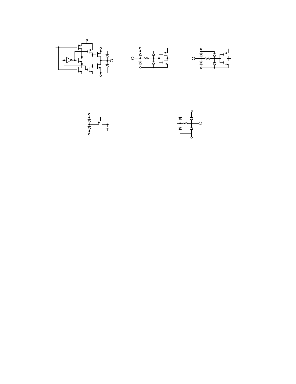
Figure 2. Equivalent Circuits
AVSS
c. CLK
AVDD
AVSS
–8–
REV. 0
Typical Performance Characteristics–A
SNR – dBFS
SFDR – dBc
SNR – dBc
100
80
60
40
dBFS AND dBc
50
70
90
A
IN
– dBFS
–30
–25 –20
–15 –10
0
–5
SFDR – dBFS
D9226
(AVDD = 5.0 V, DRVDD = 3.0 V, f
V
= 2.0 V, unless otherwise noted.)
REF
0
–10
–20
–30
–40
–50
–60
dBFS
–70
–80
–90
–100
–110
–120
0
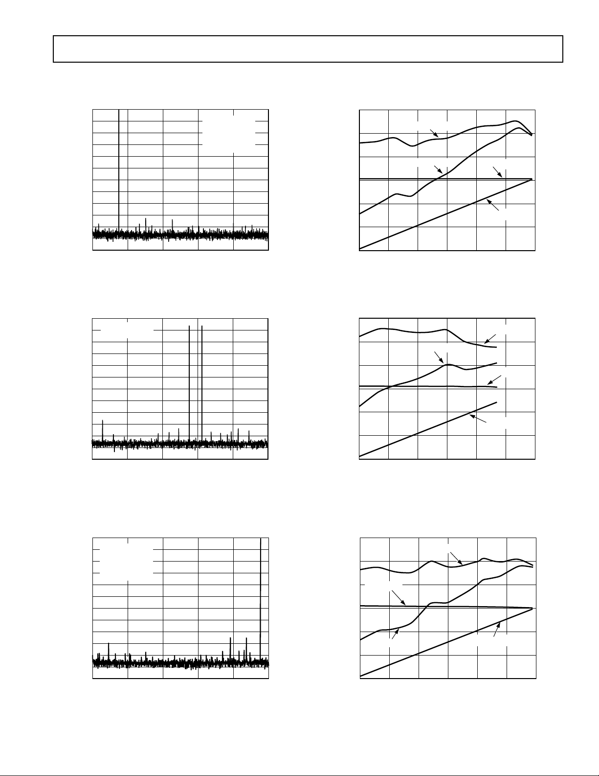
TPC 1. Single-Tone 8K FFT with fIN = 5 MHz
0
SNR = 70.4dBFS
–10
SFDR = 87.5dBFS
–20
–30
–40
–50
–60
dBFS
–70
–80
–90
–100
–110
–120
0
FREQUENCY – MHz
= 65 MSPS with CLK Stabilizer Enabled, TA = 25ⴗC, 2 V Differential Input Span, VCM = 2.5 V, AIN = –0.5 dBFS,
SAMPLE
100
FREQUENCY – MHz
SNR = 69.9dBc
SINAD = 69.8dBc
ENOB = 11.4BITS
THD = –86.4dBc
SFDR = 88.7dBc
90
80
70
dBFS AND dBc
60
50
32.56.5 13 19.5 26
40
–30
–25 –20
SFDR – dBFS
SFDR – dBc
–15 –10
– dBFS
A
IN
SNR – dBFS
SNR – dBc
TPC 4. Single-Tone SNR/SFDR vs. AIN with fIN = 5 MHz
32.56.5 13 19.5 26
–5
0
TPC 2. Dual-Tone 8K FFT with f
f
= 20 MHz (A
IN–2
0
–10
–20
–30
–40
–50
–60
dBFS
–70
–80
–90
–100
–110
–120
0 32.56.5 13 19.5 26
IN–1 = AIN–2
SNR = 69.5dBc
SINAD = 69.4dBc
ENOB = 11.3BITS
THD = –85dBc
SFDR = 87.6dBc
FREQUENCY – MHz
TPC 3. Single-Tone 8K FFT with fIN = 31 MHz
REV. 0
= –6.5 dBFS)
= 18 MHz and
IN–1
TPC 5. Dual-Tone SNR/SFDR vs. AIN with f
and f
= 20 MHz
IN–2
100
90
80
70
dBFS AND dBc
60
50
40
–30
SNR – dBFS
SFDR – dBc
–25 –20
SFDR – dBFS
–15 –10
– dBFS
A
IN
IN–1
SNR – dBc
–5
TPC 6. Single-Tone SNR/SFDR vs. AIN with fIN = 31 MHz
–9–
= 18 MHz
0
 Loading...