

Analog Devices AD9225 b Datasheet
Complete 12-Bit, 25 MSPS
Monolithic A/D Converter
AD9225
FEATURES
Monolithic 12-Bit, 25 MSPS ADC
Low Power Dissipation: 280 mW
Single 5 V Supply
No Missing Codes Guaranteed
Differential Nonlinearity Error: 0.4 LSB
Complete On-Chip Sample-and-Hold Amplifier and
Voltage Reference
Signal-to-Noise and Distortion Ratio: 71 dB
Spurious-Free Dynamic Range: –85 dB
Out-of-Range Indicator
Straight Binary Output Data
28-Lead SOIC
28-Lead SSOP
Compatible with 3 V Logic
GENERAL DESCRIPTION
The AD9225 is a monolithic, single-supply, 12-bit, 25 MSPS
analog-to-digital converter with an on-chip, high performance
sample-and-hold amplifier and voltage reference. The AD9225
uses a multistage differential pipelined architecture with output
error correction logic to provide 12-bit accuracy at 25 MSPS
data rates, and guarantees no missing codes over the full operating temperature range.
The AD9225 combines a low cost, high speed CMOS process
and a novel architecture to achieve the resolution and speed of
existing bipolar implementations at a fraction of the power
consumption and cost.
The input of the AD9225 allows for easy interfacing to both
imaging and communications systems. With the device’s truly
differential input structure, the user can select a variety of input
ranges and offsets, including single-ended applications. The
dynamic performance is excellent.
The sample-and-hold amplifier (SHA) is well suited for both
multiplexed systems that switch full-scale voltage levels in successive channels and sampling single-channel inputs at frequencies
up to and well beyond the Nyquist rate.
The AD9225’s wideband input, combined with the power and
cost savings over previously available monolithics, suits applications in communications, imaging, and medical ultrasound.
The AD9225 has an on-board programmable reference. An
external reference can also be chosen to suit the dc accuracy
and temperature drift requirements of an application.
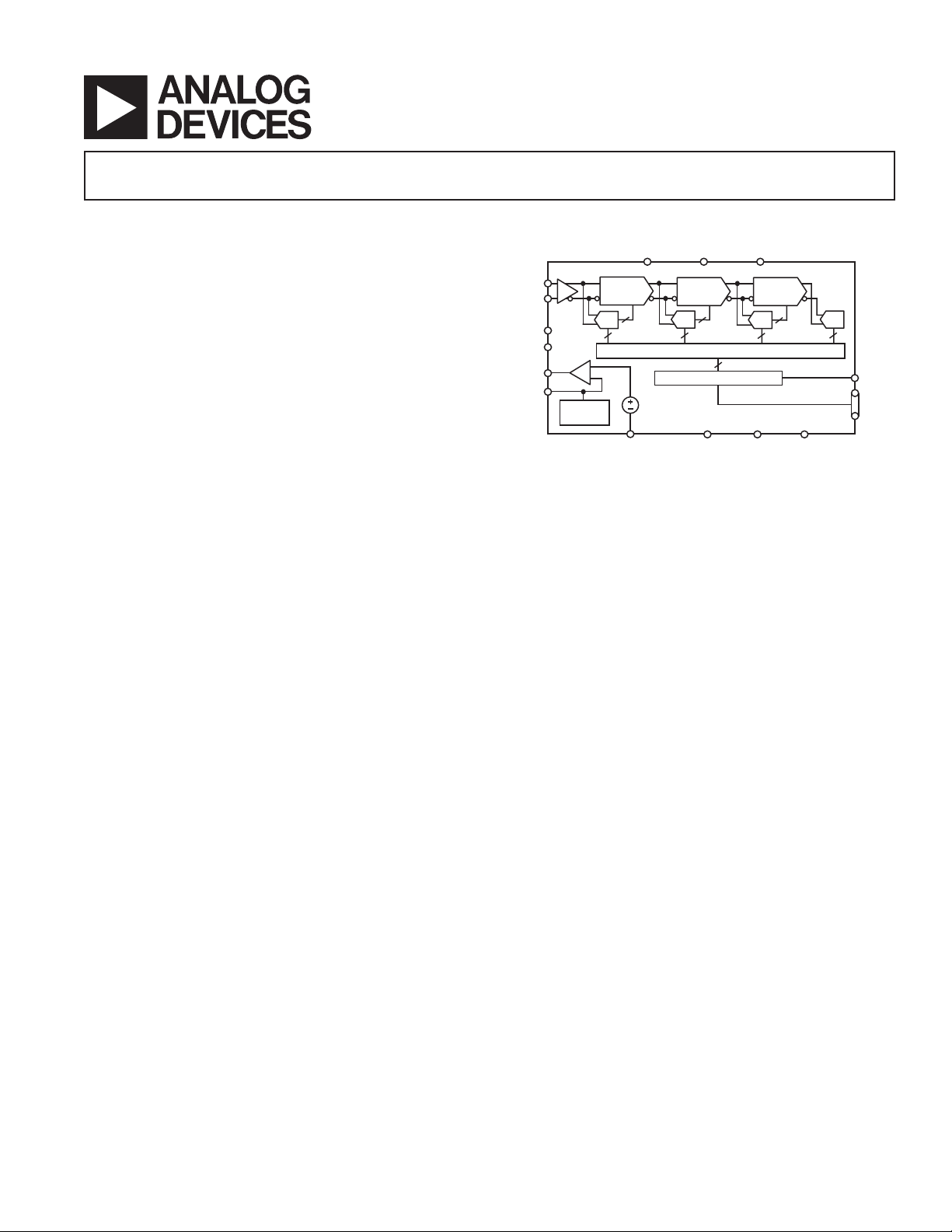
FUNCTIONAL BLOCK DIAGRAM
VINA
VINB
CAPT
CAPB
VREF
SENSE
SHA
MODE
SELECT
MDAC1
GAIN = 16
ADC
5
REFCOM
CLK
5
1V
AVDD
MDAC2
GAIN = 4
ADC
3
DIGITAL CORRECTION LOGIC
OUTPUT BUFFERS
DRVDD
MDAC3
GAIN = 4
3
ADC
3
12
AD9225
AVSS
DRVSS
3
CML
ADC
4
OTR
BIT 1
(MSB)
BIT 12
(LSB)
A single clock input is used to control all internal conversion
cycles. The digital output data is presented in straight binary
output format. An out-of-range signal indicates an overflow
condition that can be used with the most significant bit to determine low or high overflow.
PRODUCT HIGHLIGHTS
The AD9225 is fabricated on a very cost effective CMOS process. High speed precision analog circuits are combined with
high density logic circuits.
The AD9225 offers a complete, single-chip sampling, 12-bit,
25 MSPS analog-to-digital conversion function in 28-lead
SOIC and SSOP packages.
Low Power—The AD9225 at 280 mW consumes a fraction of
the power presently available in monolithic solutions.
On-Board Sample-and-Hold Amplifier (SHA)—The versatile SHA input can be configured for either single-ended or
differential inputs.
Out-of-Range (OTR)—The OTR output bit indicates when
the input signal is beyond the AD9225’s input range.
Single Supply—The AD9225 uses a single 5 V power supply,
simplifying system power supply design. It also features a separate digital driven supply line to accommodate 3 V and 5 V logic
families.
Pin Compatibility—The AD9225 is pin compatible with the
AD9220, AD9221, AD9223, and AD9224 ADCs.
REV. B
Information furnished by Analog Devices is believed to be accurate and
reliable. However, no responsibility is assumed by Analog Devices for its
use, nor for any infringements of patents or other rights of third parties that
may result from its use. No license is granted by implication or otherwise
under any patent or patent rights of Analog Devices. Trademarks and
registered trademarks are the property of their respective owners.
One Technology Way, P.O. Box 9106, Norwood, MA 02062-9106, U.S.A.
Tel: 781/329-4700 www.analog.com
Fax: 781/326-8703 © 2003 Analog Devices, Inc. All rights reserved.

AD9225–SPECIFICATIONS
DC SPECIFICATIONS
(AVDD = 5 V, DRVDD = 5 V, f
unless otherwise noted.)
= 25 MSPS, VREF = 2.0 V, VINB = 2.5 V dc, T
SAMPLE
MIN
to T
MAX
,
Parameter Min Typ Max Unit
RESOLUTION 12 Bits
MAX CONVERSION RATE 25 MHz
INPUT REFERRED NOISE
VREF = 1.0 V 0.35 LSB rms
VREF = 2.0 V 0.17 LSB rms
ACCURACY
Integral Nonlinearity (INL) ±1.0 ±2.5 LSB
Differential Nonlinearity (DNL) ±0.4 ±1.0 LSB
No Missing Codes 12 Bits Guaranteed
Zero Error (@ 25∞C) ±0.3 ±0.6 % FSR
Gain Error (@ 25∞C)
Gain Error (@ 25∞C)
1
2
±0.5 ±2.2 % FSR
±0.4 ±1.7 % FSR
TEMPERATURE DRIFT
Zero Error ±2 ppm/∞C
Gain Error
Gain Error
1
2
±26 ppm/∞C
±0.4 ppm/∞C
POWER SUPPLY REJECTION
AVDD (+5 V ± 0.25 V) ±0.1 ±0.35 % FSR
ANALOG INPUT
Input Span 2 V p-p
4V p-p
Input (VINA or VINB) Range 0 V
AVDD V
Input Capacitance 10 pF
INTERNAL VOLTAGE REFERENCE
Output Voltage (1 V Mode) 1.0 V
Output Voltage Tolerance (1 V Mode) ±5 ±17 mV
Output Voltage (2.0 V Mode) 2.0 V
Output Voltage Tolerance (2.0 V Mode) ±10 ±35 mV
Output Current (Available for External Loads) 1.0 mA
Load Regulation
3
1.0 3.4 mV
REFERENCE INPUT RESISTANCE 8 kW
POWER SUPPLIES
Supply Voltages
AVDD 4.75 5 5.25 V (±5% AVDD Operating)
DRVDD 2.85 5.25 V (±5% DRVDD Operating)
Supply Currents
IAVDD 65 72.5 mA
IDRVDD 2.0 4.0 mA
POWER CONSUMPTION
External Reference 280 310 mW (VREF = 1 V)
335 373 mW (VREF = 2 V)
Internal Reference 290 mW (VREF = 1 V)
345 mW (VREF = 2 V)
NOTES
1
Includes internal voltage reference error.
2
Excludes internal voltage reference error.
3
Load regulation with 1 mA load current (in addition to that required by the AD9225).
Specifications subject to change without notice.
REV. B–2–

AD9225
AC SPECIFICATIONS
(AVDD = 5 V, DRVDD = 5 V, f
otherwise noted.)
= 25 MSPS, VREF = 2.0 V, T
SAMPLE
MIN
to T
, Differential Input unless
MAX
Parameter Min Typ Max Unit
SIGNAL-TO-NOISE AND DISTORTION RATIO (S/N+D)
f
= 2.5 MHz 67.4 70.7 dB
INPUT
f
= 10 MHz 66.7 69.6 dB
INPUT
SIGNAL-TO-NOISE RATIO (SNR)
f
= 2.5 MHz 69.0 71 dB
INPUT
f
= 10 MHz 68.2 70 dB
INPUT
TOTAL HARMONIC DISTORTION (THD)
f
= 2.5 MHz –82 –72 dB
INPUT
f
= 10 MHz –81 –71.5 dB
INPUT
SPURIOUS FREE DYNAMIC RANGE
= 2.5 MHz 73 –85 dB
f
INPUT
= 10 MHz 72.5 –83 dB
f
INPUT
Full Power Bandwidth 105 MHz
Small Signal Bandwidth 105 MHz
Aperture Delay 1 ns
Aperture Jitter 1 ps rms
Acquisition to Full-Scale Step 10 ns
Specifications subject to change without notice.
DIGITAL SPECIFICATIONS
(AVDD = 5 V, DRVDD = 5 V, unless otherwise noted.)
Parameter Symbol Min Typ Max Unit
LOGIC INPUTS
High Level Input Voltage V
Low Level Input Voltage V
High Level Input Current (V
Low Level Input Current (V
= DRVDD) I
IN
= 0 V) I
IN
Input Capacitance C
IH
IL
IH
IL
IN
3.5 V
1.0 V
–10 +10 mA
–10 +10 mA
5pF
LOGIC OUTPUTS
High Level Output Voltage (IOH = 50 mA) V
High Level Output Voltage (I
Low Level Output Voltage (I
Low Level Output Voltage (I
= 0.5 mA) V
OH
= 1.6 mA) V
OL
= 50 mA) V
OL
Output Capacitance C
OH
OH
OL
OL
OUT
4.5 V
2.4 V
0.4 V
0.1 V
5pF
LOGIC OUTPUTS (with DRVDD = 3 V)
High Level Output Voltage (IOH = 50 mA) V
High Level Output Voltage (I
Low Level Output Voltage (I
= 0.5 mA) V
OH
= 1.6 mA) V
OL
Low Level Output Voltage (IOL = 50 mA) V
Specifications subject to change without notice.
OH
OH
OL
OL
2.95 V
2.80 V
0.4 V
0.05 V
(T
to T
SWITCHING SPECIFICATIONS
MIN
with AVDD = 5 V, DRVDD = 5 V, CL = 20 pF)
MAX
Parameter Symbol Min Typ Max Unit
Clock Period* t
CLOCK Pulse Width High t
CLOCK Pulse Width Low t
Output Delay t
C
CH
CL
OD
40 ns
18 ns
18 ns
13 ns
Pipeline Delay (Latency) 3 Clock Cycles
*The clock period may be extended to 1 ms without degradation in specified performance @ 25 ∞C.
Specifications subject to change without notice.
REV. B
–3–
AD9225
ABSOLUTE MAXIMUM RATINGS*
With
Pin Name Respect to Min Max Unit
AVDD AVSS –0.3 +6.5 V
DRVDD DRVSS –0.3 +6.5 V
AVSS DRVSS –0.3 +0.3 V
AVDD DRVDD –6.5 +6.5 V
REFCOM AVSS –0.3 +0.3 V
CLK AVSS –0.3 AVDD + 0.3 V
Digital Outputs DRVSS –0.3 DRVDD + 0.3 V
VINA, VINB AVSS –0.3 AVDD + 0.3 V
VREF AVSS –0.3 AVDD + 0.3 V
SENSE AVSS –0.3 AVDD + 0.3 V
CAPB, CAPT AVSS –0.3 AVDD + 0.3 V
Junction Temperature 150 ∞C
Storage Temperature –65 +150 ∞C
Lead Temperature (10 sec) 300 ∞C
*Stresses above those listed under Absolute Maximum Ratings may cause permanent damage to the device. This is a
stress rating only; functional operation of the device at these or any other conditions above those indicated in the
operational sections of this specification is not implied. Exposure to absolute maximum ratings for extended periods
may affect device reliability.
ANALOG
INPUT
INPUT
CLOCK
DATA
OUTPUT
S1
t
CH
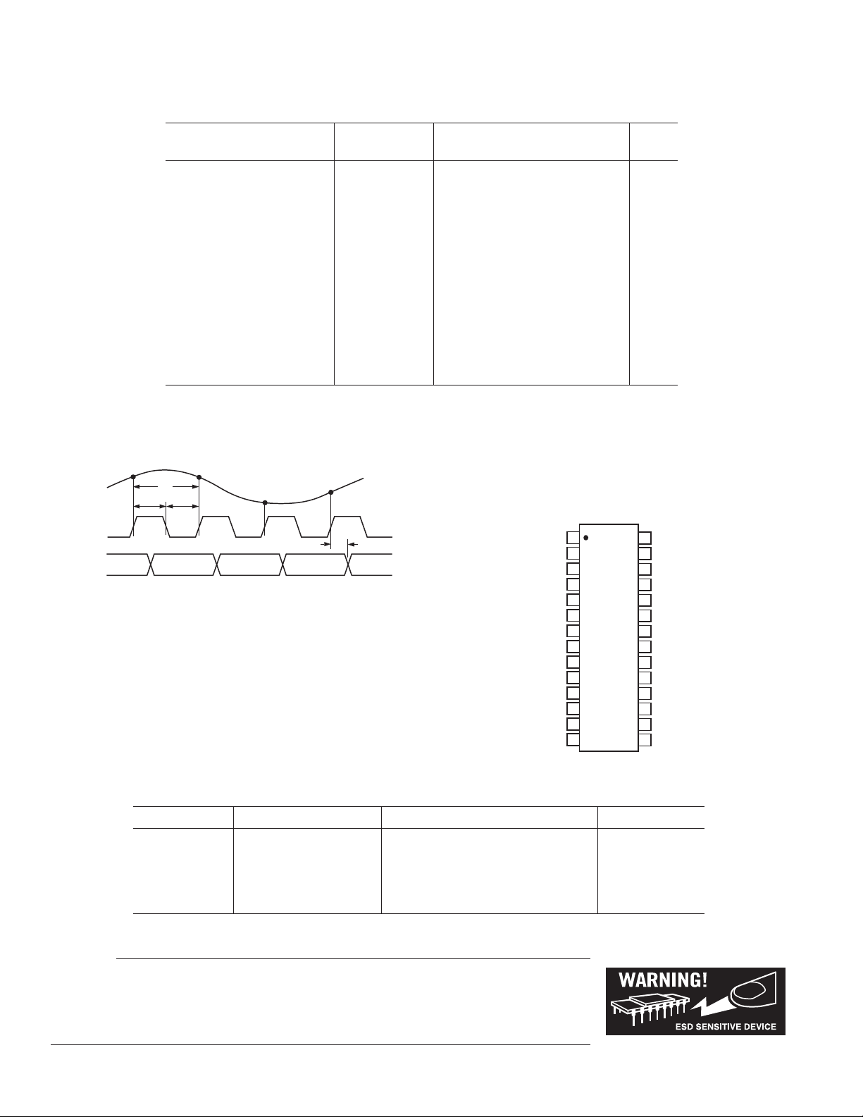
Figure 1. Timing Diagram
S2
t
C
t
CL
S3
S4
t
OD
DATA 1
PIN CONFIGURATION
28-Lead SOIC and SSOP
CLK
1
(LSB) BIT 12
(MSB ) BIT 1
BIT 11
BIT 10
BIT 9
BIT 8
BIT 7
BIT 6
BIT 5
BIT 4
BIT 3
BIT 2
OTR
2
3
4
5
6
AD9225
7
TOP VIEW
(Not to Scale)
8
9
10
11
12
13
14
28
27
26
25
24
23
22
21
20
19
18
17
16
15
DRVDD
DRVSS
AVDD
AVSS
VINB
VINA
CML
CAPT
CAPB
REFCOM
VREF
SENSE
AVSS
AVDD
ORDERING GUIDE
Model Temperature Range Package Description Package Option
AD9225AR –40∞C to +85∞C 28-Lead Wide Body Small Outline R-28
AD9225ARRL –40∞C to +85∞C 28-Lead Wide Body Small Outline R-28
AD9225ARS –40∞C to +85∞C 28-Lead Shrink Small Outline RS-28
AD9225ARSRL –40∞C to +85∞C 28-Lead Shrink Small Outline RS-28
AD9225-EB Evaluation Board
CAUTION
ESD (electrostatic discharge) sensitive device. Electrostatic charges as high as 4000 V readily
accumulate on the human body and test equipment and can discharge without detection. Although the
AD9225 features proprietary ESD protection circuitry, permanent damage may occur on devices
subjected to high energy electrostatic discharges. Therefore, proper ESD precautions are recommended
to avoid performance degradation or loss of functionality.
REV. B–4–

PIN FUNCTION DESCRIPTIONS
Pin Number Mnemonic Description
1 CLK Clock Input Pin
2BIT 12 Least Significant Data Bit (LSB)
3–12 BIT 11–2 Data Output Bit
13 BIT 1 Most Significant Data Bit (MSB)
14 OTR Out of Range
15, 26 AVDD 5 V Analog Supply
16, 25 AVSS Analog Ground
17 SENSE Reference Select
18 VREF Input Span Select (Reference I/O)
19 REFCOM Reference Common (AVSS)
20 CAPB Noise Reduction Pin
21 CAPT Noise Reduction Pin
22 CML Common-Mode Level (Midsupply)
23 VINA Analog Input Pin (+)
24 VINB Analog Input Pin (–)
27 DRVSS Digital Output Driver Ground
28 DRVDD 3 V to 5 V Digital Output Driver Supply
AD9225
TERMINOLOGY
Integral Nonlinearity (INL)
INL refers to the deviation of each individual code from a line
drawn from negative full scale through positive full scale. The
point used as negative full scale occurs 1/2 LSB before the first
code transition. Positive full scale is defined as a level 1 1/2 LSB
beyond the last code transition. The deviation is measured from
the middle of each particular code to the true straight line.
Differential Nonlinearity (DNL, No Missing Codes)
An ideal ADC exhibits code transitions that are exactly 1 LSB
apart. DNL is the deviation from this ideal value. Guaranteed
no missing codes to 12-bit resolution indicates that all 4096
codes, respectively, must be present over all operating ranges.
Zero Error
The major carry transition should occur for an analog value
1/2 LSB below VINA = VINB. Zero error is defined as the
deviation of the actual transition from that point.
Gain Error
The first code transition should occur at an analog value 1/2 LSB
above negative full scale. The last transition should occur at an
analog value 1 1/2 LSB below the nominal full scale. Gain error
is the deviation of the actual difference between first and last
code transitions and the ideal difference between first and last
code transitions.
Temperature Drift
The temperature drift for zero error and gain error specifies the
maximum change from the initial (25∞C) value to the value at
T
or T
MIN
Power Supply Rejection
MAX
.
The specification shows the maximum change in full scale from
the value with the supply at the minimum limit to the value with
the supply at its maximum limit.
Aperture Jitter
Aperture jitter is the variation in aperture delay for successive
samples and is manifested as noise on the input to the ADC.
Aperture Delay
Aperture delay is a measure of the sample-and-hold amplifier
(SHA) performance and is measured from the rising edge of the
clock input to when the input signal is held for conversion.
Signal-to-Noise and Distortion Ratio (S/N+D, SINAD)
S/N+D is the ratio of the rms value of the measured input
signal to the rms sum of all other spectral components below
the Nyquist frequency, including harmonics but excluding dc.
The value for S/N+D is expressed in decibels.
Effective Number of Bits (ENOB)
For a sine wave, SINAD can be expressed in terms of the number of bits. Using the following formula,
N = (SINAD – 1.76)/6.02
it is possible to get a measure of performance expressed as N,
the effective number of bits.
The effective number of bits for a device for sine wave inputs at
a given input frequency can be calculated directly from its measured SINAD.
Total Harmonic Distortion (THD)
THD is the ratio of the rms sum of the first six harmonic components to the rms value of the measured input signal and is
expressed as a percentage or in decibels.
Signal-to-Noise Ratio (SNR)
SNR is the ratio of the rms value of the measured input signal to
the rms sum of all other spectral components below the Nyquist
frequency, excluding the first six harmonics and dc. The value
for SNR is expressed in decibels.
Spurious-Free Dynamic Range (SFDR)
SFDR is the difference in dB between the rms amplitude of the
input signal and the peak spurious signal.
REV. B
–5–
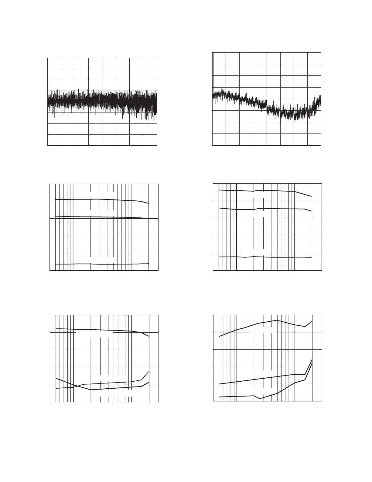
AD9225–Typical Performance Characteristics
(AVDD, DRVDD = 5 V, fS = 25 MHz (50% Duty Cycle), unless otherwise noted.)
1.00
0.75
0.50
0.25
0.00
Title
–0.25
–0.50
–0.75
–1.00
04095511
75
70
65
1022 1533 2044 2555 3066 3577
Title
TPC 1. Typical DNL
0.5dB 2V INT REF
6dB 2V INT REF
2.00
1.50
1.00
0.50
0.50
1.00
1.50
2.00
70
65
60
0
TITLE
511
1022 1533 2044 2555 3066 3577 40950
TPC 4. Typical INL
0.5dB INT 1V
6dB INT 1V
60
SINAD (dB)
55
20dB 2V INT REF
50
1
FREQUENCY (MHz)
10
TPC 2. SINAD vs. Input Frequency (Input Span = 4.0 V p-p,
V
= 2.5 V Differential Input)
CM
–60
–65
–70
THD (dB)
–75
–80
–85
20.0dB 2V INT REF
6.0dB 2V INT REF
0.5dB 2V INT REF
1
FREQUENCY (MHz)
10
55
SINAD (dB)
50
45
20dB INT 1V
1
FREQUENCY (MHz)
10
TPC 5. SINAD vs. Input Frequency (Input Span = 2 V p-p
V
= 2.5 V Differential Input)
CM
–60
1
20dB INT 1V
6dB INT 1V
0.5dB INT 1V
FREQUENCY (MHz)
10
–65
–70
THD (dB)
–75
–80
–85
TPC 3. THD vs. Input Frequency (Input Span = 4.0 V p-p,
= 2.5 V Differential Input)
V
CM
TPC 6. THD vs. Input Frequency (Input Span = 2 V p-p,
= 2.5 V Differential Input)
V
CM
REV. B–6–
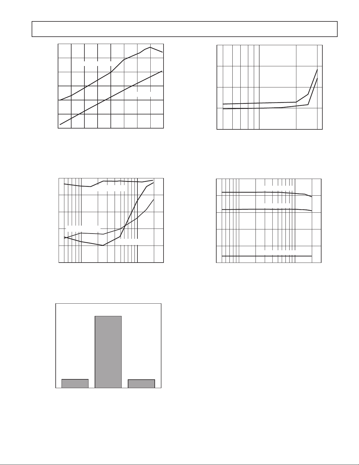
AD9225
90
80
70
60
50
SNR AND SFDR (dBFS)
40
30
–40
SFDR INT 2V REF
SNR INT 2V REF
–35
–30 –25 –20 –15 –10 –5 0
A
(dB)
IN
TPC 7. SNR/SFDR vs. AIN (Input Amplitude)
(f
= 12.5 MHz, Input Span = 4.0 V p-p, VCM = 2.5 V
IN
Differential Input)
–65
20.0dB 2V INT REF
–70
–75
–70
–75
–80
THD (dB)
INT 1V REF
–85
–90
INT 2V REF
10
FREQUENCY (MHz)
TPC 10. THD vs. Sample Rate, (AIN = –0.5 dB,
= 2.5 V, Input Span = 4.0 V p-p Differential Input)
V
CM
75
0.5dB 2V INT REF
70
6.0dB 2V INT REF
65
THD (dB)
6.0dB 2V INT REF
–80
–85
–90
1
FREQUENCY (MHz)
0.5dB 2V INT REF
10
TPC 8. THD vs. Input Frequency (Input Span =
4.0 V p-p, V
ITS
H
= 2.5 V Single-Ended Input)
CM
246447
3299
N – 1 N
B
IN
4206
N + 1
TPC 9. Grounded-Input Histogram (Input Span =
40 V p-p)
SNR (dB)
60
55
20.0dB 2V INT REF
50
1
FREQUENCY (MHz)
10
TPC 11. SNR vs. Input Frequency (Input Span =
4.0 V p-p, V
= 2.5 V Single-Ended Input)
CM
REV. B
–7–
AD9225
INTRODUCTION
The AD9225 is a high performance, complete single-supply
12-bit ADC. The analog input range of the AD9225 is highly
flexible, allowing for both single-ended or differential inputs
of varying amplitudes that can be ac-coupled or dc-coupled.
The AD9225 utilizes a four-stage pipeline architecture with a
wideband input sample-and-hold amplifier (SHA) implemented
on a cost-effective CMOS process. Each stage of the pipeline,
excluding the last stage, consists of a low resolution flash ADC
connected to a switched capacitor DAC and interstage residue
amplifier (MDAC). The residue amplifier amplifies the difference between the reconstructed DAC output and the flash input
for the next stage in the pipeline. One bit of redundancy is used
in each of the stages to facilitate digital correction of flash errors.
The last stage simply consists of a flash ADC.
The pipeline architecture allows a greater throughput rate at the
expense of pipeline delay or latency. This means that while the
converter is capable of capturing a new input sample every clock
cycle, it actually takes three clock cycles for the conversion to
be fully processed and appear at the output. This latency is not
a concern in most applications. The digital output, together
with the out-of-range indicator (OTR), is latched into an
output buffer to drive the output pins. The output drivers of
the AD9225 can be configured to interface with 5 V or 3.3 V
logic families.
The AD9225 uses both edges of the clock in its internal timing
circuitry (see Figure 1 and Specifications tables for exact timing
requirements). The ADC samples the analog input on the rising
edge of the clock input. During the clock low time (between the
falling edge and rising edge of the clock), the input SHA is in
the sample mode; during the clock high time it is in hold mode.
System disturbances just prior to the rising edge of the clock
and/or excessive clock jitter may cause the input SHA to acquire
the wrong value, and should be minimized.
ANALOG INPUT AND REFERENCE OVERVIEW
Figure 2 is a simplified model of the AD9225. It highlights the
relationship between the analog inputs, VINA and VINB, and the
reference voltage, VREF. Like the voltage applied to the top of
the resistor ladder in a flash ADC, the value VREF defines the
maximum input voltage to the ADC core. The minimum input
voltage to the ADC core is automatically defined to be –VREF.
VINA
VINB
AD9225
V
CORE
+VRE F
ADC
CORE
–VREF
12
Figure 2. Equivalent Functional Input Circuit
The addition of a differential input structure gives the user an
additional level of flexibility that is not possible with traditional
flash converters. The input stage allows the user to easily configure the inputs for either single-ended operation or differential
operation. The A/D converter’s input structure allows the dc
offset of the input signal to be varied independently of the input
span of the converter. Specifically, the input to the ADC core is
the difference of the voltages applied at the VINA and VINB
input pins. Therefore, the equation
VCORE = VINA – VINB (1)
defines the output of the differential input stage and provides
the input to the ADC core.
The voltage, VCORE, must satisfy the condition
–VREF £ VCORE £ VREF (2)
where VREF is the voltage at the VREF pin.
While an infinite combination of VINA and VINB inputs exist
that satisfy Equation 2, there is an additional limitation placed
on the inputs by the power supply voltages of the AD9225. The
power supplies bound the valid operating range for VINA and
VINB. The condition
AVSS – 0.3 V < VINA < AVDD + 0.3 V (3)
AVSS – 0.3 V < VINB < AVDD + 0.3 V
where AVSS is nominally 0 V and AVDD is nominally 5 V,
defines this requirement. The range of valid inputs for VINA
and VINB is any combination that satisfies both Equations
2 and 3.
For additional information showing the relationships among
VINA, VINB, VREF, and the digital output of the AD9225, see
Table IV.
Refer to Table I and Table II at the end of this section for a summary of the various analog input and reference configurations.
ANALOG INPUT OPERATION
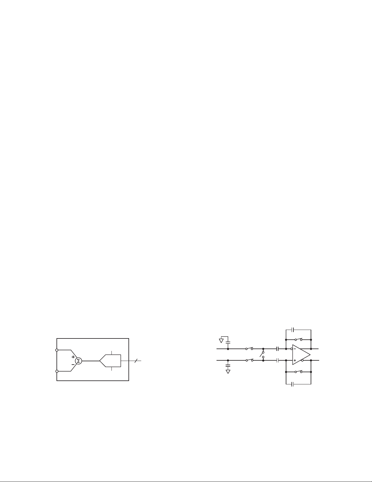
Figure 3 shows the equivalent analog input of the AD9225,
which consists of a differential sample-and-hold amplifier. The
differential input structure of the SHA is highly flexible, allowing the devices to be easily configured for either a differential or
single-ended input. The dc offset, or common-mode voltage, of
the input(s) can be set to accommodate either single-supply or
dual-supply systems. Also, note that the analog inputs, VINA
and VINB, are interchangeable, with the exception that reversing the inputs to the VINA and VINB pins results in a polarity
inversion.
C
H
Q
S2
Q
S2
C
H
VINA
VINB
+
C
PIN
Q
S1
C
PAR
Q
S1
–
C
PIN
C
PAR
C
S
Q
C
H1
S
Figure 3. Simplified Input Circuit
The AD9225 has a wide input range. The input peaks may be
moved to AVDD or AVSS before performance is compromised.
This allows for much greater flexibility when selecting singleended drive schemes. Op amps and ac coupling clamps can be
set to available reference levels rather than be dictated according
to what the ADC needs.
REV. B–8–
 Loading...