Quad, 10-Bit, 40/65 MSPS
V
V
V
V
V
V
V
V
A
V
Data Sheet
FEATURES
4 ADCs integrated into 1 package
94 mW ADC power per channel at 65 MSPS
SNR = 60 dB (to Nyquist)
ENOB = 9.7 bits
SFDR = 78 dBc (to Nyquist)
Excellent linearity
DNL = ±0.2 LSB (typical)
INL = ±0.3 LSB (typical)
Serial LVDS (ANSI-644, default)
Low power, reduced signal option (similar to IEEE 1596.3)
Data and frame clock outputs
315 MHz full-power analog bandwidth
2 V p-p input voltage range
1.8 V supply operation
Serial port control
Full-chip and individual-channel power-down modes
Flexible bit orientation
Built-in and custom digital test pattern generation
Programmable clock and data alignment
Programmable output resolution
Standby mode
APPLICATIONS
Medical imaging and nondestructive ultrasound
Portable ultrasound and digital beam-forming systems
Quadrature radio receivers
Diversity radio receivers
Tap e dr ive s
Optical networking
Test equipment
GENERAL DESCRIPTION
Serial LVDS 1.8 V ADC
AD9219
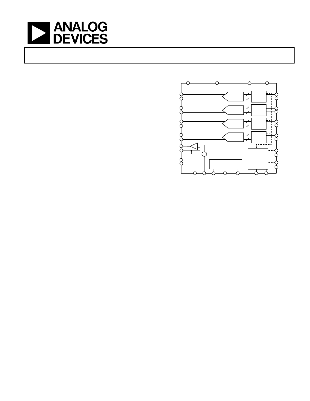
FUNCTIONAL BLOCK DIAGRAM
DD
IN + A
IN – A
IN + B
IN – B
IN + C
IN – C
IN + D
IN – D
VREF
SENSE
REFT
REFB
REF
SELECT
The ADC automatically multiplies the sample rate clock for the
appropriate LVDS serial data rate. A data clock output (DCO) for
capturing data on the output and a frame clock output (FCO)
for signaling a new output byte are provided. Individual-channel
power-down is supported and typically consumes less than
2 mW when all channels are disabled.
The ADC contains several features designed to maximize
flexibility and minimize system cost, such as programmable
clock and data alignment and programmable digital test pattern
generation. The available digital test patterns include built-in
deterministic and pseudorandom patterns, along with custom userdefined test patterns entered via the serial port interface (SPI).
+
–
AGND
PDWN
AD9219
0.5V
SERI AL P ORT
INTERFACE
SDIO/ODMRBIAS
CSB
PIPELINE
ADC
PIPELINE
ADC
PIPELINE
ADC
PIPELINE
ADC
Figure 1.
DRVDD
10
10
10
10
SCLK/DTP
DRGND
SERIAL
LVDS
SERIAL
LVDS
SERIAL
LVDS
SERIAL
LVDS
DATA RATE
MULTI PLI ER
CLK+
CLK–
D + A
D – A
D + B
D – B
D + C
D – C
D + D
D – D
FCO+
FCO–
DCO+
DCO–
5726-001
The AD9219 is a quad, 10-bit, 40/65 MSPS analog-to-digital converter (ADC) with an on-chip sample-and-hold circuit designed
for low cost, low power, small size, and ease of use. The product
operates at a conversion rate of up to 65 MSPS and is optimized for
outstanding dynamic performance and low power in applications
where a small package size is critical.
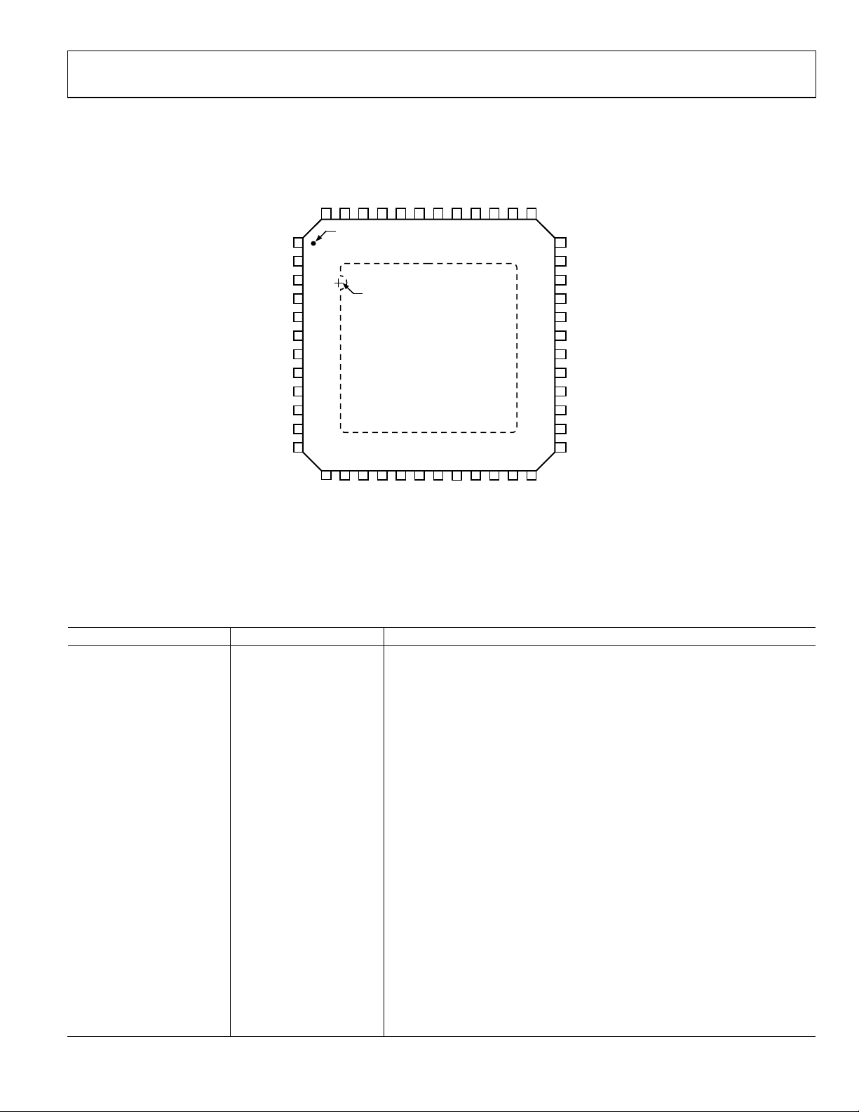
The AD9219 is available in an RoHS compliant, 48-lead LFCSP. It is
specified over the industrial temperature range of −40°C to +85°C.
PRODUCT HIGHLIGHTS
1. Small Footprint. Four ADCs are contained in a small, space-
saving package.
2. Low power of 94 mW/channel at 65 MSPS.
The ADC requires a single 1.8 V power supply and LVPECL-/
CMOS-/LVDS-compatible sample rate clock for full performance
operation. No external reference or driver components are
required for many applications.
3. Ease of Use. A data clock output (DCO) is provided that
operates at frequencies of up to 390 MHz and supports
double data rate (DDR) operation.
4. User Flexibility. The SPI control offers a wide range of flexible
features to meet specific system requirements.
5. Pin-Compatible Family. This includes the AD9287 (8-bit),
Rev. E
Information furnished by Analog Devices is believed to be accurate and reliable. However, no
responsibility is assumed by Analog Devices for its use, nor for any infringements of patents or other
rights of third parties that may result from its use. Specifications subject to change without notice. No
license is granted by implication or otherwise under any patent or patent rights of Analog Devices.
Trademarks and registered trademarks are the property of their respective owners.
AD9228 (12-bit), and AD9259 (14-bit).
One Technology Way, P.O. Box 9106, Norwood, MA 02062-9106, U.S.A.
Tel: 781.329.4700 www.analog.com
Fax: 781.461.3113 ©2006–2011 Analog Devices, Inc. All rights reserved.

AD9219 Data Sheet
TABLE OF CONTENTS
Features .............................................................................................. 1
Analog Input Considerations ................................................... 20
Applications ....................................................................................... 1
General Description ......................................................................... 1
Functional Block Diagram .............................................................. 1
Product Highlights ........................................................................... 1
Revision History ............................................................................... 2
Specifications ..................................................................................... 4
AC Specifications .......................................................................... 5
Digital Specifications ................................................................... 6
Switching Specifications .............................................................. 7
Timing Diagrams .............................................................................. 8
Absolute Maximum Ratings .......................................................... 10
Thermal Impedance ................................................................... 10
ESD Caution ................................................................................ 10
Pin Configuration and Function Descriptions ........................... 11
Equivalent Circuits ......................................................................... 13
Clock Input Considerations ...................................................... 23
Serial Port Interface (SPI) .............................................................. 31
Hardware Interface ..................................................................... 31
Memory Map .................................................................................. 33
Reading the Memory Map Table .............................................. 33
Reserved Locations .................................................................... 33
Default Values ............................................................................. 33
Logic Levels ................................................................................. 33
Evaluation Board ............................................................................ 37
Power Supplies ............................................................................ 37
Input Signals................................................................................ 37
Output Signals ............................................................................ 37
Default Operation and Jumper Selection Settings ................. 38
Alternative Analog Input Drive Configuration...................... 39
Outline Dimensions ....................................................................... 53
Typical Performance Characteristics ........................................... 15
Theory of Operation ...................................................................... 20
REVISION HISTORY
12/11—Rev. D to Rev. E
Added Exposed Pad Notation to Figure 5 ................................... 11
Changes to Output Signals Section and Figure 71 ..................... 37
Change to Default Operation and Jumper Selection Settings
Section .............................................................................................. 38
Change to Figure 74 ....................................................................... 41
Changed LFCSP_WQ to LFCSP_VQ Throughout .................... 53
Added Endnote 2 in Ordering Guide .......................................... 53
5/10—Rev. C to Rev. D
Updated Outline Dimensions ....................................................... 52
Changes to Ordering Guide .......................................................... 52
4/10—Rev. B to Rev. C
Changes to Table 16 ........................................................................ 33
Updated Outline Dimensions ....................................................... 52
7/07—Rev. A to Rev. B
Changes to Figure 2 and Figure 4 ................................................... 7
Changes to Table 17 ........................................................................ 50
Rev. E | Page 2 of 56
Ordering Guide .......................................................................... 53
5/07—Rev. 0 to Rev. A
Changes to Features .......................................................................... 1
Changes to Logic Output (SDIO/ODM) Section .......................... 5
Added Endnote 3 to Table 3 ............................................................. 5
Changes to Pipeline Latency ............................................................ 6
Changes to Figure 2 to Figure 4 ....................................................... 7
Changes to Figure 10 ...................................................................... 12
Changes to Figure 15, Figure 23 to Figure 26 Captions ............ 14
Changes to Figure 16, Figure 37, Figure 39, and Figure 40....... 14
Added Figure 46 and Figure 47 .................................................... 20
Change to Figure 50 ....................................................................... 21
Changes to Figure 51 ...................................................................... 21
Changes to Clock Duty Cycle Considerations Section ............. 22
Changes to Power Dissipation and
Power-Down Mode Section .......................................................... 23
Changes to Figure 58 ...................................................................... 23
Changes to Figure 61 to Figure 63 Captions ............................... 25
Change to Table 8 ........................................................................... 25
Changes to Digital Outputs and Timing Section ....................... 26
Changes to Table 9 Endnote .......................................................... 26
Added Table 10 ............................................................................... 27
Deleted Figure 62 and Figure 63 .................................................. 27

Data Sheet AD9219
Changes to RBIAS Pin Section ...................................................... 28
Changes to Figure 67 ...................................................................... 29
Changes to Hardware Interface Section ....................................... 30
Added Figure 68 .............................................................................. 31
Changes to Table 15 ........................................................................ 31
Changes to Reading the Memory Map Table Section ................ 32
Changes to Output Signals Section ............................................... 36
Changes to Figure 71 ...................................................................... 36
Changes to Default Operation and
Jumper Selection Settings Section ................................................ 37
Changes to Alternative Analog Input Drive Configuration
Section .............................................................................................. 38
Changes to Figure 74 ...................................................................... 40
Changes to Table 17 ........................................................................ 48
Changes to Ordering Guide ........................................................... 52
4/06—Revision 0: Initial Version
Rev. E | Page 3 of 56

AD9219 Data Sheet
SPECIFICATIONS
AVDD = 1.8 V, DRVDD = 1.8 V, 2 V p-p differential input, 1.0 V internal reference, AIN = −0.5 dBFS, unless otherwise noted.
Table 1.
AD9219-40 AD9219-65
Parameter1 Temperature Min Typ Max Min Typ Max Unit
RESOLUTION 10 10 Bits
ACCURACY
No Missing Codes Full Guaranteed Guaranteed
Offset Error Full ±1 ±8 ±1 ±8 mV
Offset Matching Full ±2 ±8 ±2 ±8 mV
Gain Error Full ±0.4 ±1.2 ±2 ±3.5 % FS
Gain Matching Full ±0.3 ±0.7 ±0.3 ±0.7 % FS
Differential Nonlinearity (DNL) Full ±0.1 ±0.4 ±0.15 ±0.4 LSB
Integral Nonlinearity (INL) Full ±0.15 ±0.4 ±0.3 ±0.75 LSB
TEMPERATURE DRIFT
Offset Error Full ±2 ±2 ppm/°C
Gain Error Full ±17 ±17 ppm/°C
Reference Voltage (1 V Mode) Full ±21 ±21 ppm/°C
REFERENCE
Output Voltage Error (V
Load Regulation at 1.0 mA (V
Input Resistance Full 6 6 kΩ
ANALOG INPUTS
Differential Input Voltage (V
Common-Mode Voltage Full AVDD/2 AVDD/2 V
Differential Input Capacitance Full 7 7 pF
Analog Bandwidth, Full Power Full 315 315 MHz
POWER SUPPLY
AVDD Full 1.7 1.8 1.9 1.7 1.8 1.9 V
DRVDD Full 1.7 1.8 1.9 1.7 1.8 1.9 V
I
Full 130 142 177 190 mA
AVDD
I
Full 30 32 33 37 mA
DRVDD
Total Power Dissipation (Including Output Drivers) Full 295 313 378 408 mW
Power-Down Dissipation Full 2 5.8 2 5.8 mW
Standby Dissipation2 Full 72 72 mW
CROSSTALK Full −100 −100 dB
CROSSTALK (Overrange Condition)3 Full −100 −100 dB
1
See the AN-835 Application Note, Understanding High Speed ADC Testing and Evaluation, for definitions and for details of how these tests were completed.
2
Can be controlled via the SPI.
3
Overrange condition is specific with 6 dB of the full-scale input range.
= 1 V) Full ±2 ±30 ±2 ±30 mV
REF
= 1 V) Full 3 3 mV
REF
= 1 V) Full 2 2 V p-p
REF
Rev. E | Page 4 of 56

Data Sheet AD9219
AC SPECIFICATIONS
AVDD = 1.8 V, DRVDD = 1.8 V, 2 V p-p differential input, 1.0 V internal reference, AIN = −0.5 dBFS, unless otherwise noted.
Table 2.
AD9219-40 AD9219-65
Parameter1 Temperature Min Typ Max Min Typ Max Unit
SIGNAL-TO-NOISE RATIO (SNR)
fIN = 2.4 MHz Full 61.2 60.2 dB
fIN = 19.7 MHz Full 60.0 60.5 60.2 dB
fIN = 35 MHz Full 61.0 59.0 60.2 dB
fIN = 70 MHz Full 60.9 60.1 dB
SIGNAL-TO-NOISE AND DISTORTION RATIO (SINAD)
fIN = 2.4 MHz Full 61.1 60.1 dB
fIN = 19.7 MHz Full 59.8 60.3 60.1 dB
fIN = 35 MHz Full 60.9 58.8 60.0 dB
fIN = 70 MHz Full 60.8 59.8 dB
EFFECTIVE NUMBER OF BITS (ENOB)
fIN = 2.4 MHz Full 9.87 9.71 Bits
fIN = 19.7 MHz Full 9.67 9.76 9.71 Bits
fIN = 35 MHz Full 9.84 9.51 9.71 Bits
fIN = 70 MHz Full 9.82 9.69 Bits
SPURIOUS-FREE DYNAMIC RANGE (SFDR)
fIN = 2.4 MHz Full 84 78 dBc
fIN = 19.7 MHz Full 71 82 78 dBc
fIN = 35 MHz Full 80 68 77 dBc
fIN = 70 MHz Full 79 72 dBc
WORST HARMONIC (Second or Third)
fIN = 2.4 MHz Full −84 −80 dBc
fIN = 19.7 MHz Full −82 −71 −80 dBc
fIN = 35 MHz Full −80 −77 −68 dBc
fIN = 70 MHz Full −79 −72 dBc
WORST OTHER (Excluding Second or Third)
fIN = 2.4 MHz Full −90 −78 dBc
fIN = 19.7 MHz Full −90 −77 −78 dBc
fIN = 35 MHz Full −90 −80 −70 dBc
fIN = 70 MHz Full −88 −80 dBc
TWO-TONE INTERMODULATION DISTORTION (IMD)—
AIN1 and AIN2 = −7.0 dBFS
f
= 15 MHz, f
IN1
f
= 70 MHz, f
IN1
1
See the AN-835 Application Note, Understanding High Speed ADC Testing and Evaluation, for definitions and for details of how these tests were completed.
= 16 MHz 25°C 81.5 78.1 dBc
IN2
= 71 MHz 25°C 79.5 74.5 dBc
IN2
Rev. E | Page 5 of 56

AD9219 Data Sheet
DIGITAL SPECIFICATIONS
AVDD = 1.8 V, DRVDD = 1.8 V, 2 V p-p differential input, 1.0 V internal reference, AIN = −0.5 dBFS, unless otherwise noted.
Table 3.
AD9219-40 AD9219-65
Parameter1 Temperature Min Typ Max Min Typ Max Unit
CLOCK INPUTS (CLK+, CLK−)
Logic Compliance CMOS/LVDS/LVPECL CMOS/LVDS/LVPECL
Differential Input Voltage2 Full 250 250 mV p-p
Input Common-Mode Voltage Full 1.2 1.2 V
Input Resistance (Differential) 25°C 20 20 kΩ
Input Capacitance 25°C 1.5 1.5 pF
LOGIC INPUTS (PDWN, SCLK/DTP)
Logic 1 Voltage Full 1.2 3.6 1.2 3.6 V
Logic 0 Voltage Full 0 0.3 0.3 V
Input Resistance 25°C 30 30 kΩ
Input Capacitance 25°C 0.5 0.5 pF
LOGIC INPUT (CSB)
Logic 1 Voltage Full 1.2 3.6 1.2 3.6 V
Logic 0 Voltage Full 0 0.3 0.3 V
Input Resistance 25°C 70 70 kΩ
Input Capacitance 25°C 0.5 0.5 pF
LOGIC INPUT (SDIO/ODM)
Logic 1 Voltage Full 1.2 DRVDD + 0.3 1.2 DRVDD + 0.3 V
Logic 0 Voltage Full 0 0.3 0 0.3 V
Input Resistance 25°C 30 30 kΩ
Input Capacitance 25°C 2 2 pF
LOGIC OUTPUT (SDIO/ODM)3
Logic 1 Voltage (IOH = 800 μA) Full 1.79 1.79 V
Logic 0 Voltage (IOL = 50 μA) Full 0.05 0.05 V
DIGITAL OUTPUTS (D + x, D − x), (ANSI-644)
Logic Compliance LVDS LV DS
Differential Output Voltage (VOD) Full 247 454 247 454 mV
Output Offset Voltage (VOS) Full 1.125 1.375 1.125 1.375 V
Output Coding (Default) Offset binary Offset binary
DIGITAL OUTPUTS (D + x, D − x),
(Low Power, Reduced Signal Option)
Logic Compliance LVDS LV DS
Differential Output Voltage (VOD) Full 150 250 150 250 mV
Output Offset Voltage (VOS) Full 1.10 1.30 1.10 1.30 V
Output Coding (Default) Offset binary Offset binary
1
See the AN-835 Application Note, Understanding High Speed ADC Testing and Evaluation, for definitions and for details of how these tests were completed.
2
This is specified for LVDS and LVPECL only.
3
This is specified for 13 SDIO pins sharing the same connection.
Rev. E | Page 6 of 56

Data Sheet AD9219
SWITCHING SPECIFICATIONS
AVDD = 1.8 V, DRVDD = 1.8 V, 2 V p-p differential input, 1.0 V internal reference, AIN = −0.5 dBFS, unless otherwise noted.
Table 4.
AD9219-40 AD9219-65
Parameter
CLOCK3
OUTPUT PARAMETERS3
APERTURE
1
See the AN-835 Application Note, Understanding High Speed ADC Testing and Evaluation, for definitions and for details of how these tests were completed.
2
Measured on standard FR-4 material.
3
Can be adjusted via the SPI.
4
t
SAMPLE
1, 2
Temp Min Typ Max Min Typ Max Unit
Maximum Clock Rate Full 40 65 MSPS
Minimum Clock Rate Full 10 10 MSPS
Clock Pulse Width High (tEH) Full 12.5 7.7 ns
Clock Pulse Width Low (tEL) Full 12.5 7.7 ns
Propagation Delay (tPD) Full 2.0 2.5 3.5 2.0 2.5 3.5 ns
Rise Time (tR) (20% to 80%) Full 300 300 ps
Fall Time (tF) (20% to 80%) Full 300 300 ps
FCO Propagation Delay (t
DCO Propagation Delay (t
DCO to Data Delay (t
DCO to FCO Delay (t
Data to Data Skew
(t
− t
DATA-MAX
DATA-MIN
) Full 2.0 2.5 3.5 2.0 2.5 3.5 ns
FCO
)4 Full t
CPD
DATA
FRAME
)4
)4
Full (t
Full (t
SAMPLE
SAMPLE
/20) − 300 (t
/20) − 300 (t
FCO
(t
+
SAMPLE
SAMPLE
SAMPLE
t
/20)
/20) (t
/20) (t
/20) + 300 (t
SAMPLE
/20) + 300 (t
SAMPLE
/20) − 300 (t
SAMPLE
/20) − 300 (t
SAMPLE
FCO
(t
SAMPLE
SAMPLE
SAMPLE
+
ns
/20)
/20) (t
/20) (t
/20) + 300 ps
SAMPLE
/20) + 300 ps
SAMPLE
Full ±50 ±150 ±50 ±150 ps
)
Wake-Up Time (Standby) 25°C 600 600 ns
Wake-Up Time (Power-Down) 25°C 375 375 μs
Pipeline Latency Full 8 8 CLK
cycles
Aperture Delay (tA) 25°C 500 500 ps
Aperture Uncertainty (Jitter) 25°C <1 <1 ps rms
Out-of-Range Recovery Time 25°C 1 2 CLK
cycles
/20 is based on the number of bits divided by 2 because the delays are based on half duty cycles.
Rev. E | Page 7 of 56
AD9219 Data Sheet
TIMING DIAGRAMS
N – 1
VIN ± x
CLK–
CLK+
DCO–
DCO+
FCO–
FCO+
D – x
D + x
t
A
N
t
EH
t
CPD
MSB
N – 9
t
FRAME
D8
N – 9D7N – 9
t
FCO
t
PD
t
EL
D6
N – 9
D5
N – 9
t
DATA
D4
N – 9
D3
N – 9
D2
N – 9
D1
N – 9
D0
N – 9
MSB
N – 8
D8
N – 8D7N – 8
D6
N – 8
D5
N – 8
05726-040
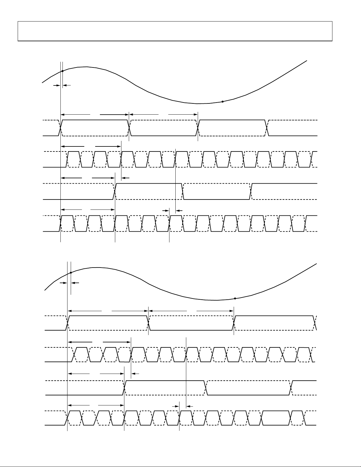
Figure 2. 10-Bit Data Serial Stream, MSB First (Default)
N – 1
VIN ± x
CLK–
CLK+
DCO–
DCO+
FCO–
FCO+
D – x
D + x
t
A
N
t
EH
t
CPD
t
FCO
t
PD
t
FRAME
MSB
D10
N – 9
N – 9D9N – 9D8N – 9D7N – 9D6N – 9D5N – 9D4N – 9D3N – 9D2N – 9D1N – 9D0N – 9
Figure 3. 12-Bit Data Serial Stream, MSB First
t
EL
t
DATA
D10
MSB
N – 8
N – 8
05726-039
Rev. E | Page 8 of 56
Data Sheet AD9219
V
N – 1
IN ± x
t
A
N
CLK–
CLK+
DCO–
DCO+
FCO–
FCO+
D – x
D + x
t
EH
t
CPD
t
FCO
t
PD
t
FRAME
LSB
N – 9D0N – 9D1N – 9D2N – 9D3N – 9D4N – 9D5N – 9D6N – 9D7N – 9D8N – 9
t
EL
t
DATA
LSB
N – 8D0N – 8
D1
N – 8
D2
N – 8
05726-041
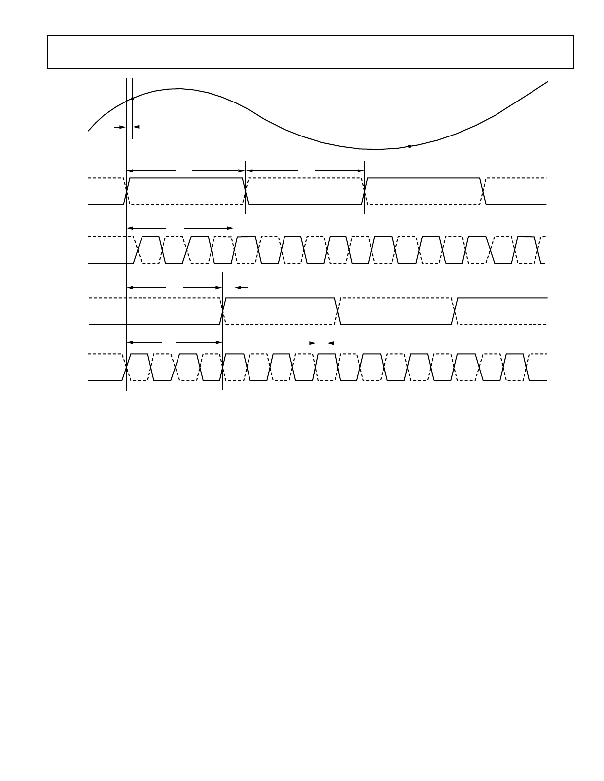
Figure 4. 10-Bit Stream, LSB First
Rev. E | Page 9 of 56
AD9219 Data Sheet
ABSOLUTE MAXIMUM RATINGS
Table 5.
With
Parameter
ELECTRICAL
AVDD AGND −0.3 V to +2.0 V
DRVDD DRGND −0.3 V to +2.0 V
AGND DRGND −0.3 V to +0.3 V
AVDD DRVDD −2.0 V to +2.0 V
Digital Outputs
(D + x, D − x, DCO+,
DCO−, FCO+, FCO−)
CLK+, CLK− AGND −0.3 V to +3.9 V
VIN + x, VIN − x AGND −0.3 V to +2.0 V
SDIO/ODM AGND −0.3 V to +2.0 V
PDWN, SCLK/DTP, CSB AGND −0.3 V to +3.9 V
REFT, REFB, RBIAS AGND −0.3 V to +2.0 V
VREF, SENSE AGND −0.3 V to +2.0 V
ENVIRONMENTAL
Operating Temperature
Range (Ambient)
Maximum Junction
Temperature
Lead Temperature
(Soldering, 10 sec)
Storage Temperature
Range (Ambient)
Respect To
DRGND −0.3 V to +2.0 V
−40°C to +85°C
150°C
300°C
−65°C to +150°C
Rating
Stresses above those listed under Absolute Maximum Ratings
may cause permanent damage to the device. This is a stress
rating only; functional operation of the device at these or any
other conditions above those indicated in the operational
section of this specification is not implied. Exposure to absolute
maximum rating conditions for extended periods may affect
device reliability.
THERMAL IMPEDANCE
Table 6.
Air Flow Velocity (m/sec) θ
0.0 24 °C/W
1.0 21 12.6 1.2 °C/W
2.5 19 °C/W
1
θJA for a 4-layer PCB with solid ground plane (simulated). Exposed pad
soldered to PCB.
1
θ
JA
JB
θJC Unit
ESD CAUTION
Rev. E | Page 10 of 56
Data Sheet AD9219
PIN CONFIGURATION AND FUNCTION DESCRIPTIONS
VIN – C
VIN + C
47
48
PIN 1
1
AVDD
2
AVDD
3
VIN – D
VIN + D
4
5
AVDD
6
AVDD
7
CLK–
8
CLK+
9
AVDD
10
AVDD
11
DRGND
12
DRVDD
NOTES
1. THE EXPOSED PAD MUST BE CONNECTED TO ANALOG GROUND.
INDICATO R
14
13
D – D
D + D
REFT
REFB
43
44
AD9219
TOP VIEW
17
18
D – B
D + B
VREF
42
19
D – A
AVDD
AVDD
45
46
EXPOSED PADDLE, PIN 0
(BOTTO M OF P ACKAGE)
16
15
D – C
D + C
SENSE
41
20
D + A
RBIAS
40
FCO–
AVDD
39
222123
FCO+
VIN + B
38
DCO–
VIN – B
37
36
AVDD
35
AVDD
34
VIN – A
33
VIN + A
32
AVDD
31
PDWN
30
CSB
29
SDIO/ODM
28
SCLK/DTP
27
AVDD
26
DRGND
25
DRVDD
24
DCO+
05726-003
Figure 5. 48-Lead LFCSP Pin Configuration, Top View
Table 7. Pin Function Descriptions
Pin No. Mnemonic Description
0 AGND Analog Ground (Exposed Paddle)
1, 2, 5, 6, 9, 10, 27, 32,
35, 36, 39, 45, 46
11, 26
12, 25
3
4
7
AVDD 1.8 V Analog Supply
DRGND Digital Output Driver Ground
DRVDD 1.8 V Digital Output Driver Supply
VIN − D ADC D Analog Input Complement
VIN + D ADC D Analog Input True
CLK− Input Clock Complement
8 CLK+ Input Clock True
13
14
15
16
17
18
D − D ADC D Digital Output Complement
D + D ADC D Digital Output True
D − C ADC C Digital Output Complement
D + C ADC C Digital Output True
D − B ADC B Digital Output Complement
D + B ADC B Digital Output True
19 D − A ADC A Digital Output Complement
20 D + A ADC A Digital Output True
21
22
23
24
FCO− Frame Clock Output Complement
FCO+ Frame Clock Output True
DCO− Data Clock Output Complement
DCO+ Data Clock Output True
28 SCLK/DTP Serial Clock/Digital Test Pattern
29
SDIO/ODM Serial Data IO/Output Driver Mode
Rev. E | Page 11 of 56

AD9219 Data Sheet
Pin No. Mnemonic Description
30
31 PDWN Power-Down
33
34
37
38
40
41
42
43
44
47
48
CSB Chip Select Bar
VIN + A ADC A Analog Input True
VIN − A ADC A Analog Input Complement
VIN − B ADC B Analog Input Complement
VIN + B ADC B Analog Input True
RBIAS External resistor sets the internal ADC core bias current
SENSE Reference Mode Selection
VREF Voltage Reference Input/Output
REFB Differential Reference (Negative)
REFT Differential Reference (Positive)
VIN + C ADC C Analog Input True
VIN − C ADC C Analog Input Complement
Rev. E | Page 12 of 56
Data Sheet AD9219
A
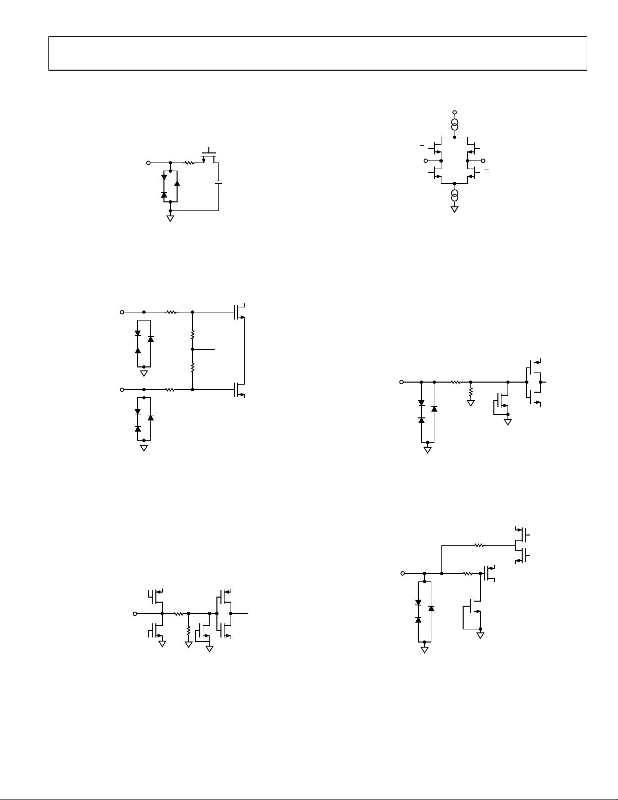
EQUIVALENT CIRCUITS
DRVDD
VIN ± x
Figure 6. Equivalent Analog Input Circuit
CLK+
CLK–
10
10k
10k
10
1.25V
V
D– D+
V
05726-030
DRGND
V
V
05726-005
Figure 9. Equivalent Digital Output Circuit
SCLK/DTP
ND PDWN
1k
30k
Figure 7. Equivalent Clock Input Circuit
SDIO/ODM
350
30k
Figure 8. Equivalent SDIO/ODM Input Circuit
05726-032
05726-033
Figure 10. Equivalent SCLK/DTP and PDWN Input Circuit
RBIAS
05726-035
100
05726-031
Figure 11. Equivalent RBIAS Circuit
Rev. E | Page 13 of 56
AD9219 Data Sheet
A
V
DD
70k
CSB
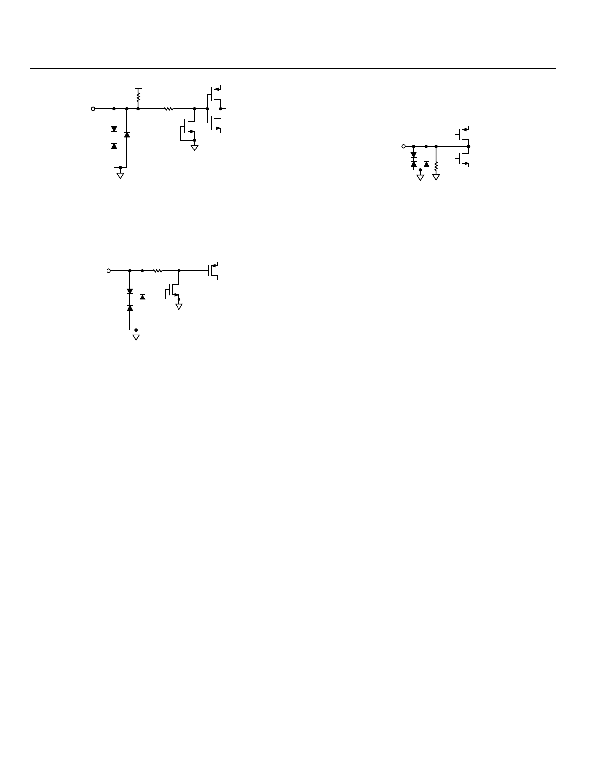
Figure 12. Equivalent CSB Input Circuit
1k
VREF
6k
05726-034
05726-037
Figure 14. Equivalent VREF Circuit
SENSE
1k
05726-036
Figure 13. Equivalent SENSE Circuit
Rev. E | Page 14 of 56
Data Sheet AD9219
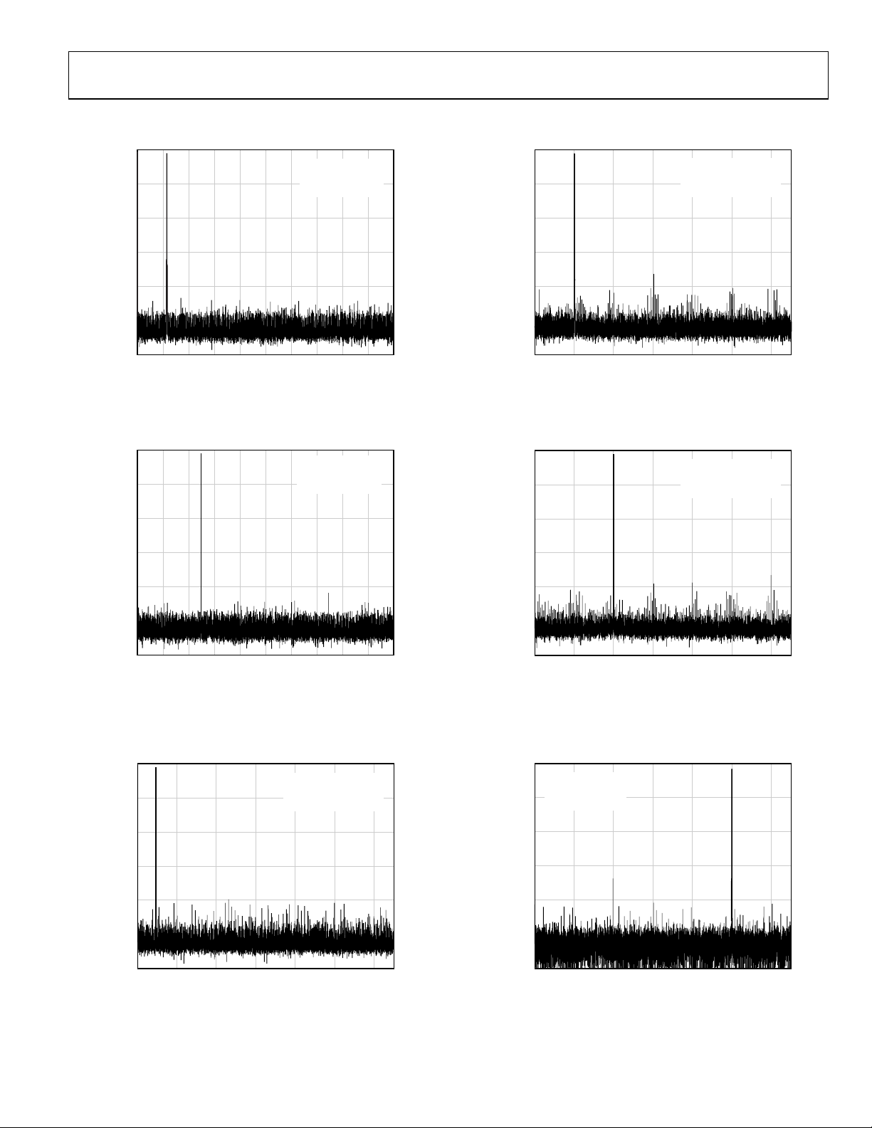
TYPICAL PERFORMANCE CHARACTERISTICS
–20
0
AIN = –0.5dBF S
SNR = 61.22dB
ENOB = 9.88 BI TS
SFDR = 85.20d Bc
–20
0
AIN = –0.5dBF S
SNR = 59.81dB
ENOB = 9.64 BI TS
SFDR = 70.02dBc
–40
–60
–80
AMPLITUDE (dBFS)
–100
–120
0 2 4 6 8 10 12 14 16 18 20
FREQUENCY (MHz)
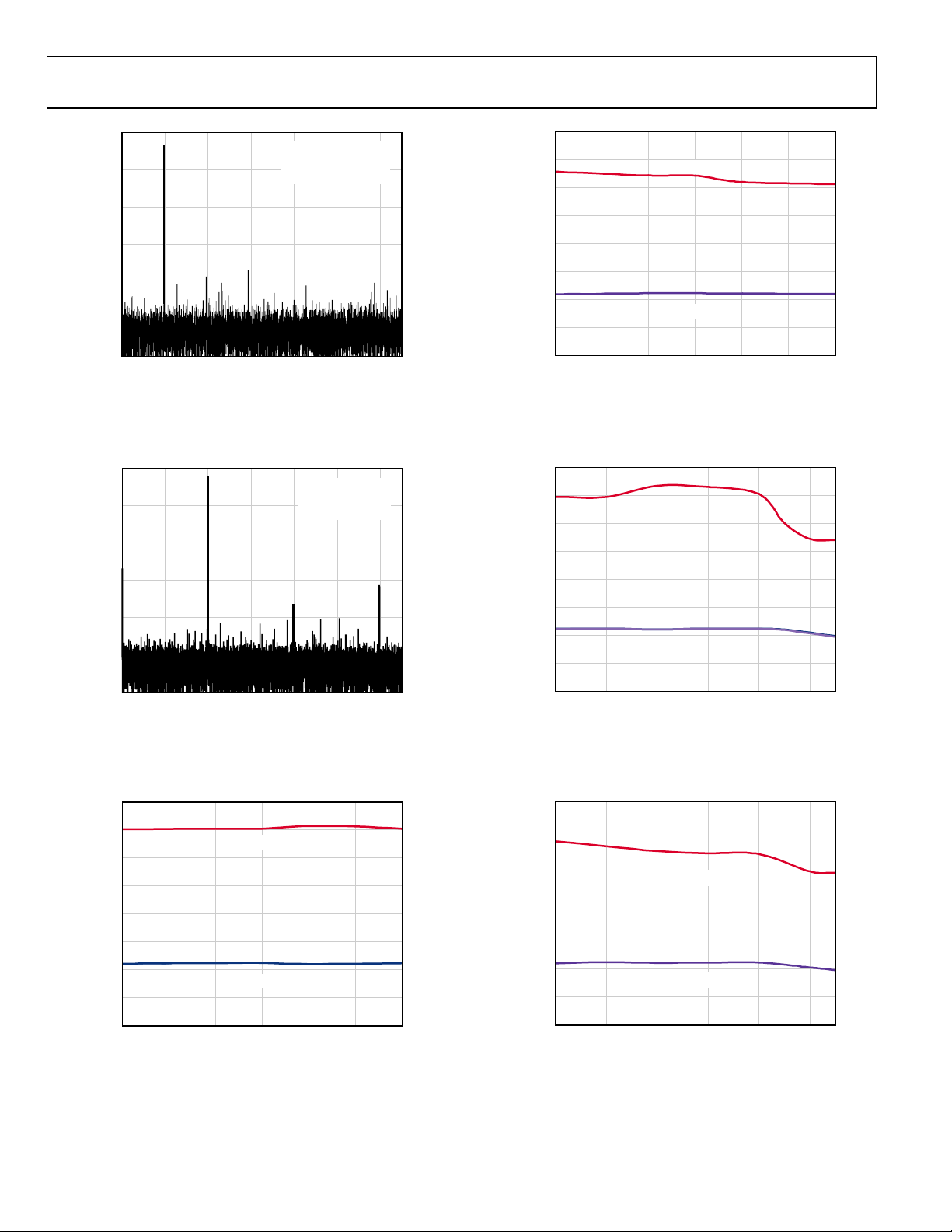
Figure 15. Single-Tone 32k FFT with fIN = 2.4 MHz, f
0
–20
–40
–60
–80
AMPLITUDE (dBFS)
–100
AIN = –0.5dBFS
SNR = 59.87dB
ENOB = 9.65 BITS
SFDR = 81.68d Bc
SAMPLE
= 40 MSPS
–40
–60
–80
AMPLITUDE (dBFS)
–100
05726-056
–120
030520251510
FREQUENCY (MHz )
Figure 18. Single-Tone 32k FFT with fIN = 70 MHz, f
0
–20
–40
–60
–80
AMPLITUDE (dBFS)
–100
ENOB = 9.62 BI TS
SFDR = 70.86dBc
= 65 MSPS
SAMPLE
AIN = –0.5dBF S
SNR = 59.68dB
05726-058
–120
0 2 4 6 8 10 12 14 16 18 20
FREQUENCY (MHz)
Figure 16. Single-Tone 32k FFT with fIN = 35 MHz, f
0
AIN = –0.5dBF S
SNR = 59.93dB
–20
–40
–60
–80
AMPLITUDE ( dBFS)
–100
–120
030520251510
FREQUENCY (MHz )
ENOB = 9.66 BI TS
SFDR = 77.58dBc
Figure 17. Single-Tone 32k FFT with fIN = 2.3 MHz, f
SAMPLE
SAMPLE
= 40 MSPS
= 65 MSPS
05726-076
05726-057
–120
030520251510
FREQUENCY (MHz )
Figure 19. Single-Tone 32k FFT with fIN = 120 MHz, f
0
AIN = –0.5dBF S
SNR = 59.93dB
ENOB = 9.66 BI TS
–20
SFDR = 63.51d Bc
–40
–60
–80
AMPLITUDE (dBFS)
–100
–120
030520251510
FREQUENCY (MHz )
Figure 20. Single-Tone 32k FFT with fIN = 170 MHz, f
SAMPLE
SAMPLE
= 65 MSPS
= 65 MSPS
05726-059
05726-053
Rev. E | Page 15 of 56
AD9219 Data Sheet
90
85
80
75
2V p-p, SFDR
–20
–40
0
AIN = –0. 5dBFS
SNR = 56. 72dB
ENOB = 9.13 BITS
SFDR = 66. 41dBc
–60
–80
AMPLITUDE ( dBFS)
–100
–120
030520251510
FREQUENCY (MHz)
Figure 21. Single-Tone 32k FFT with fIN = 190 MHz, f
0
AIN = –0.5dBF S
SNR = 58.57dB
–20
–40
–60
–80
AMPLITUDE (dBFS)
–100
–120
030520251510
FREQUENCY (MHz )
ENOB = 9.44 BI TS
SFDR = 57.95dBc
Figure 22. Single-Tone 32k FFT with fIN = 250 MHz, f
SAMPLE
SAMPLE
= 65 MSPS
= 65 MSPS
70
65
SNR/SFDR (dB)
60
55
05726-054
50
10 4015 30 352520
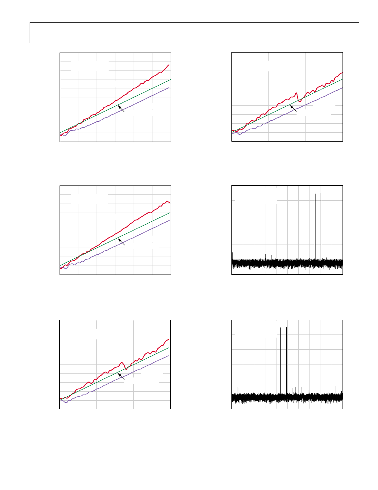
Figure 24. SNR/SFDR vs. Encode, fIN = 35 MHz, f
90
85
80
75
70
65
SNR/SFDR (dB)
60
55
05726-055
50
10 6040 503020
Figure 25. SNR/SFDR vs. Encode, fIN = 10.3 MHz, f
2V p-p, SNR
ENCODE (MSPS)
2V p-p, SFDR
2V p-p, SNR
ENCODE (MSPS)
SAMPLE
SAMPLE
05726-063
= 40 MSPS
05726-061
= 65 MSPS
90
85
80
75
70
65
SNR/SFDR (dB)
60
55
50
10 4015 30 352520
2V p-p, SFDR
2V p-p, SNR
ENCODE (MSPS)
Figure 23. SNR/SFDR vs. Encode, fIN = 10.3 MHz, f
SAMPLE
= 40 MSPS
05726-060
Rev. E | Page 16 of 56
90
85
80
75
70
65
SNR/SFDR (dB)
60
55
50
10 50 603020 40
2V p-p, SFDR
2V p-p, SNR
ENCODE (MSPS)
Figure 26. SNR/SFDR vs. Encode, fIN = 35 MHz, f
SAMPLE
05726-065
= 65 MSPS
Data Sheet AD9219
100
90
80
70
60
50
40
SNR/SF DR (dB)
30
20
10
f
=10.3MHz
IN
f
=40MSPS
SAMPLE
2V p-p, SFDR
70dB REFERENCE
0
–60 –10 0–40–50 –30 –20
ANALOG INPUT LEVEL (dBFS)
2V p-p, SNR
Figure 27. SNR/SFDR vs. Analog Input Level, fIN = 10.3 MHz, f
100
90
80
70
60
50
40
SNR/SFDR (dB)
30
20
10
Figure 28. SNR/SFDR vs. Analog Input Level, f
f
=35MHz
IN
f
=40MSPS
SAMPLE
2V p-p, SFDR
70dB REFERENCE
0
–60 –10 0–40–50 –30 –20
ANALOG INPUT LEVEL (dBFS)
= 35 MHz, f
IN
2V p-p, SNR
SAMPLE
SAMPLE
05726-062
= 40 MSPS
05726-066
= 40 MSPS
100
90
80
70
60
50
40
SNR/SFDR (dB)
30
20
10
f
=35MHz
IN
f
= 65MSPS
SAMPLE
2V p-p, SFDR
70dB REFERENCE
0
–60 –10 0–40–50 –30 –20
ANALOG INPUT LEVEL (dBFS)
2V p-p, SNR
Figure 30. SNR/SFDR vs. Analog Input Level, fIN = 35 MHz, f
0
AIN1 AND AIN2 = –7dBFS
SFDR = 82.54dBc
IMD2 = 88.33d Bc
–20
IMD3 = 81.77d Bc
–40
–60
–80
AMPLITUDE (dBFS)
–100
–120
02468101214161820
Figure 31. Two-Tone 32k FFT with f
FREQUENCY (MHz )
IN1
= 40 MSPS
f
SAMPLE
= 15 MHz and f
= 65 MSPS
SAMPLE
= 16 MHz,
IN2
05726-067
05726-048
100
90
80
70
60
50
40
SNR/SF DR (dB)
30
20
10
f
= 10.3MHz
IN
f
= 65MSPS
SAMPLE
2V p-p, SFDR
70dB REFERENCE
0
–60 –10 0–40–50 –30 –2 0
ANALOG INPUT LEVEL (dBFS)
2V p-p, SNR
Figure 29. SNR/SFDR vs. Analog Input Level, fIN = 10.3 MHz, f
SAMPLE
05726-064
= 65 MSPS
Rev. E | Page 17 of 56
0
AIN1 AND AIN2 = –7dBFS
SFDR = 79.13d Bc
IMD2 = 79.56d Bc
–20
IMD3 = 79.66d Bc
–40
–60
–80
AMPLI TUDE (d BFS)
–100
–120
0 2 4 6 8 10 12 14 16 18 20
Figure 32. Two-Tone 32k FFT with f
FREQUENCY (MHz)
IN1
= 40 MSPS
f
SAMPLE
= 70 MHz and f
= 71 MHz,
IN2
05726-049
 Loading...