Analog Devices AD9218 b Datasheet

10-Bit, 40/65/80/105 MSPS
FEATURES
Dual 10-bit, 40 MSPS, 65 MSPS, 80 MSPS, and 105 MSPS ADC
Low power: 275 mW at 105 MSPS per channel
On-chip reference and track-and-hold
300 MHz analog bandwidth each channel
SNR = 57 dB @ 41 MHz, Encode = 80 MSPS
1 V p-p or 2 V p-p analog input range each channel
3.0 V single-supply operation (2.7 V to 3.6 V)
Power-down mode for single-channel operation
Twos complement or offset binary output mode
Output data alignment mode
Pin compatible with 8-bit AD9288
–75 dBc crosstalk between channels
APPLICATIONS
Battery-powered instruments
Hand-held scopemeters
Low cost digital oscilloscopes
I and Q communications
Ultrasound equipment
A
IN
AINA
REF
IN
REF
OUT
REF
IN
A
IN
A
IN
ENCODE B
3 V Dual A/D Converter
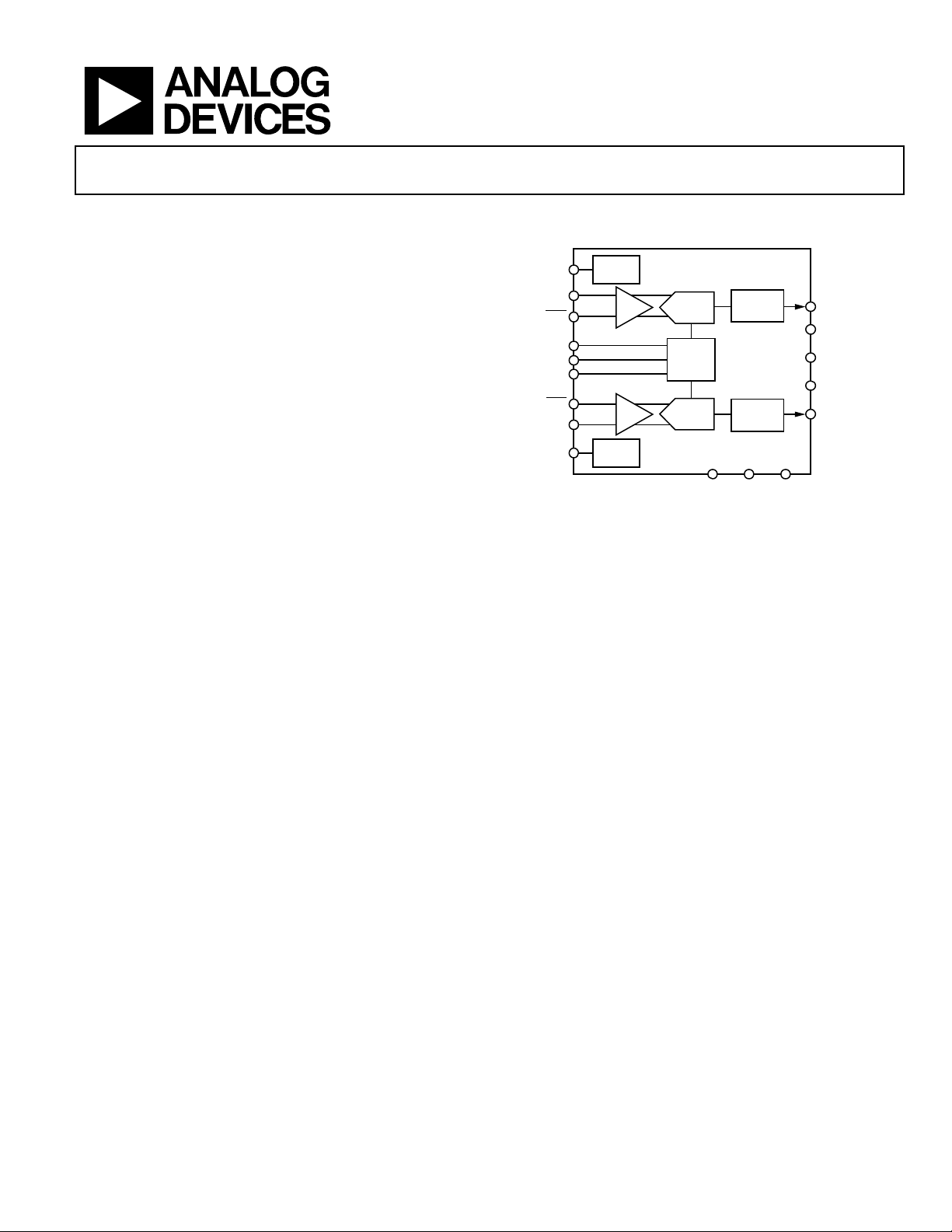
FUNCTIONAL BLOCK DIAGRAM
ADC
REF
ADC
V
Figure 1.
AD9218
/
REGISTER
10
/
REGISTER
10
D
OUTPUT
OUTPUT
GND
TIMINGENCODE A
A
A
B
B
B
T/H
T/H
TIMING
AD9218
D9A–D0
/
10
USER
SELECT NO. 1
USER
SELECT NO. 2
DATA
FORMAT/
GAIN
D9
–D0
/
B
10
V
DD
A
B
02001-B-001
GENERAL DESCRIPTION
The AD9218 is a dual 10-bit monolithic sampling analog-todigital converter with on-chip track-and-hold circuits. The
product is low cost, uses low power, is small and is easy to use.
The AD9218 operates at a 105 MSPS conversion rate with
outstanding dynamic performance over its full operating
range. Each channel can be operated independently.
The ADC requires only a single 3.0 V (2.7 V to 3.6 V) power
supply and a clock for full operation. No external reference or
driver components are required for many applications. The
digital outputs are TTL/CMOS compatible and a separate
output power supply pin supports interfacing with 3.3 V or
2.5 V logic.
The clock input is TTL/CMOS compatible and the 10-bit digital
outputs can be operated from 3.0 V (2.5 V to 3.6 V) supplies.
User-selectable options offer a combination of power-down
modes, digital data formats, and digital data timing schemes.
In power-down mode, the digital outputs are driven to a high
impedance state.
PRODUCT HIGHLIGHTS
1. Low power.
Just 275 mW power dissipation per channel at 105 MSPS.
Other speed grades proportionally scaled down while
maintaining high ac performance.
2. Pin compatibility upgrade.
Allows easy migration from 8-bit to 10-bit devices. Pin
compatible with the 8-bit AD9288 dual ADC.
3. Easy to use.
On-chip reference and user controls provide flexibility in
system design.
4. High performance.
Maintains 54 dB SNR at 105 MSPS with a Nyquist input.
5. Channel crosstalk.
Very low at –75 dBc.
6. Fabricated on an advanced CMOS process.
Available in a 48-lead low profile quad flat package
(7 mm × 7 mm LQFP) specified over the industrial
temperature range (–40°C to +85°C).
Rev. B
Information furnished by Analog Devices is believed to be accurate and reliable.
However, no responsibility is assumed by Analog Devices for its use, nor for any
infringements of patents or other rights of third parties that may result from its use.
Specifications subject to change without notice. No license is granted by implication or
otherwise under any patent or patent rights of Analog Devices. Trademarks and
registered trademarks are the property of their respective owners.
One Technology Way, P.O. Box 9106, Norwood, MA 02062-9106, U.S.A.
Tel: 781.329.4700
Fax: 781.326.8703 © 2004 Analog Devices, Inc. All rights reserved.
www.analog.com

AD9218
TABLE OF CONTENTS
Specifications..................................................................................... 3
DC Specifications ......................................................................... 3
Digital Specifications ................................................................... 4
AC Specifications.......................................................................... 5
Switching Specifications .............................................................. 6
Absolute Maximum Ratings............................................................ 8
ESD Caution.................................................................................. 8
Pin Configuration and Function Descriptions............................. 9
Te r m in o l o g y ................................................................................ 10
Equivalent Circuits..................................................................... 12
Typical Performance Characteristics........................................... 13
Theory of Operation ......................................................................18
AD9218/AD9288 Customer PCB BOM...................................... 20
Evaluation Board ............................................................................ 21
Power Connector ........................................................................ 21
Analog Inputs.............................................................................. 21
Volt a ge R ef e re n ce ....................................................................... 21
Clocking....................................................................................... 21
Data Outputs............................................................................... 21
Data Format/Gain...................................................................... 21
Timing ......................................................................................... 21
Troubleshooting.......................................................................... 25
Outline Dimensions....................................................................... 26
Ordering Guide .......................................................................... 27
Using the AD9218 ENCODE Input .........................................18
Applications.................................................................................19
REVISION HISTORY
Revision B:
1/04—Data sheet changed from REV A. to REV. B
Updated format..................................................................... Universal
Changes to General Description .......................................................1
Changes to DC Specifications............................................................ 3
Changes to Switching Specifications................................................. 6
Added AD9218/AD9288 Customer PCB BOM section............... 20
Added Evaluation Board section..................................................... 21
Revision A:
7/03—Data Sheet changed from REV. 0 to REV. A.
Updated Ordering Guide.................................................................... 6
Changes to Terminology section...................................................... .8
Changes to Figure 17b....................................................................... 19
Updated Outline Dimensions.......................................................... 24
Rev.B | Page 2 of 28

AD9218
SPECIFICATIONS
DC SPECIFICATIONS
Table 1. VDD = 3.0 V, VD = 3.0 V; external reference, unless otherwise noted.
AD9218BST-40/-65 AD9218BST-80/-105
Parameter Temp
RESOLUTION 10 10 Bits
ACCURACY
No Missing Codes1 Full VI Guaranteed, not tested Guaranteed, not tested
Offset Error2 25°C I –18 2 18 –18 2 18 LSB
Gain Error2 25°C I –2 3 8 –2 3.5 8 % FS
Differential Nonlinearity
25°C I –1 ±0.3/±0.6 1/1.3 –1 ±0.5/±0.8 1.2/1.7 LSB
(DNL)
Full VI ±0.8 ±0.6/±0.9 LSB
Integral Nonlinearity (INL) 25°C I –1/–1.6 ±0.3/±1 1/1.6 –1.35/–2.7 ±0.75/±2 +1.35/2.7 LSB
Full VI ±1 ±1/±2.3 LSB
TEMPERATURE DRIFT
Offset Error Full V 10 4 ppm/°C
Gain Error2 Full V 80 100 ppm/°C
Reference Full V 40 40 ppm/°C
REFERENCE
Internal Reference Voltage
(REFOUT) 25°C I 1.18 1.24 1.28 1.18 1.24 1.28 V
Input Resistance
Full VI 9 11 13 9 11 13 kΩ
(REFIN A, B)
ANALOG INPUTS
Differential Input Voltage
Range (A
IN, AIN
)3
Common-Mode Voltage
Full
3
Full V VD/3 VD/3 V
Input Resistance Full VI 8 10 14 8 10 14 kΩ
Input Capacitance 25°C V 3 3 pF
POWER SUPPLY
VD Full IV 2.7 3 3.6 2.7 3 3.6 V
VDD Full IV 2.7 3 3.6 2.7 3 3.6 V
Supply Currents
IVD (VD = 3.0 V)4 Full VI 108/117 113/122 172/183 175/188 mA
IVDD (VDD = 3.0 V)4 25°C V 7/11 13/17 mA
Power Dissipation DC5 Full VI 325/350 340/365 515/550 525/565 mW
IVD Power-Down Current6 Full VI 20 22 mA
Power Supply Rejection
25°C I
Ratio
1
No missing codes across industrial temperature range guaranteed for 40 MSPS, 65 MSPS, and 80 MSPS grades. No missing codes at room temperature guaranteed
for 105 MSPS grade.
2
Gain error and gain temperature coefficients are based on the ADC only (with a fixed 1.25 V external reference) -65 Grade in 2 V p-p range, -40, -85, -105 grades in
1 V p-p range.
3
A
IN
(AIN –
) = ±0.5 V in 1 V range (full scale), (AIN –
overdriven externally by a low impedance source by ±300 mV (differential drive, gain=1) or ±150 mV (differential drive, gain= 2).
4
AC power dissipation measured with rated encode and a 10.3 MHz analog input @ 0.5 dBFS, C
5
DC power dissipation measured with rated encode and a dc analog input (outputs static, IVDD = 0).
6
In power-down state IVDD = ±10 µA typical (all grades).
Test
Level
V
A
Min Typ Max Min Typ Max Unit
1 or 2
IN
) = ±1 V in 2 V range (full scale). The analog inputs will self-bias to VD/3. This common mode voltage can be
±1 ±1 mV/V
= 5 pF.
LOAD
1
V
Rev. B | Page 3 of 28

AD9218
DIGITAL SPECIFICATIONS
Table 2.VDD = 3.0 V, VD = 3.0 V; external reference, unless otherwise noted.
Test AD9218BST-40/-65 AD9218BST-80/-105
Parameter Temp Level Min Typ Max Min Typ Max Unit
DIGITAL INPUTS
Encode Input Common
Mode
Encode 1 Voltage Full VI 2 2 V
Encode 0 Voltage Full VI 0.8 0.8 V
Encode Input Resistance Full VI 1.8 2.0 2.3 1.8 2.0 2.3 kΩ
Logic 1 Voltage—S1, S2,
DFS
Logic 0 Voltage—S1, S2,
DFS
Logic 1 Current—S1 Full VI –50 ±0 50 –50 ±0 50 µA
Logic 0 Current—S1 Full VI –400 –230 –50 –400 –230 –50 µA
Logic 1 Current—S2 Full VI 50 230 400 50 230 400 µA
Logic 0 Current—S2 Full VI –50 ±0 50 –50 ±0 50 µA
Logic 1 Current—DFS Full VI 30 100 200 30 100 200 µA
Logic 0 Current—DFS Full VI –400 –230 –50 –400 –230 –50 µA
Input Capacitance—S1, S2,
Encode Inputs
Input Capacitance DFS 25°C V 4.5 4.5 pF
DIGITAL OUTPUTS
Logic 1 Voltage Full VI 2.45 2.45 V
Logic 0 Voltage Full VI 0.05 0.05 V
Output Coding Twos Complement or Offset Binary Twos Complement or Offset Binary
Full V VD/2 VD/2 V
Full VI 2 2 V
Full VI 0.8 0.8 V
25°C V 2 2 pF
Rev.B | Page 4 of 28

AD9218
AC SPECIFICATIONS
Table 3.VDD = 3.0 V, VD = 3.0 V; external reference, unless otherwise noted.
AD9218BST-40/-65 AD9218BST-80/-105
Parameter Temp
DYNAMIC PERFORMANCE1
Signal-to-Noise Ratio (SNR)
(Without Harmonics)
fIN = 10.3 MHz 25°C I 58/55 59/57 57/53 58/55 dB
fIN = Nyquist
2
25°C I –/54 59/56 55/52 57/54 dB
Signal-to-Noise Ratio (SINAD)
(With Harmonics)
fIN = 10.3 MHz 25°C I 58/54 59/56 56/52 58/53 dB
fIN = Nyquist2 25°C I –/53 59/55 55/51 57/53 dB
Effective Number of Bits
fIN = 10.3 MHz 25°C I 9.4/8.8 9.6/9.1 9.1/8.4 9.4/8.6 Bits
fIN = Nyquist2 25°C I –/8.6 9.6/8.9 9/8.3 9.3/8.6 Bits
Second Harmonic Distortion
fIN= 10.3 MHz 25°C I –72/–66 –89/–77 –69/–60 –77/–68 dBc
fIN = Nyquist2 25°C I –/–63 –89/–72 –65/–57 –76/–66 dBc
Third Harmonic Distortion
fIN = 10.3 MHz 25°C I –68/–62 –79/–68 –62/–57 –71/–63 dBc
fIN = Nyquist2 25°C I –/–60 –78/–64 –63/–57 –73/–69 dBc
Spurious Free Dynamic Range SFDR
fIN = 10.3 MHz 25°C I –68/–62 –79/–67 –62/–57 –69/–62 dBc
fIN = Nyquist2 25°C I –/–60 –78/–64 –63/–57 –70/–63 dBc
Two-Tone Intermod Distortion (IMD)
f
= 10 MHz, f
IN1
= 11 MHz 25°C V –74/–73 dBc
IN2
at –7 dBFS
f
= 30 MHz, f
IN1
= 31 MHz 25°C V –73/–73 –77/–67 dBc
IN2
at –7 dBFS
Analog Bandwidth, Full Power 25°C V 300 300 MHz
Crosstalk 25°C V –75 –75 dBc
1
AC specifications based on an analog input voltage of –0.5 dBFS at 10.3 MHz unless otherwise noted. AC specifications for -40, -80, -105 grades are tested in 1 V p-p
range and driven differentially. AC specifications for -65 grade are tested in 2 V p-p range and driven differentially.
2
The –65, –80, and –105 grades are tested close to Nyquist for that grade: 31 MHz, 39 MHz, and 51 MHz for the -65, -80, and -105 grades, respectively.
Test
Level
Min Typ Max Min Typ Max Unit
Rev. B | Page 5 of 28

AD9218
SWITCHING SPECIFICATIONS
Table 4. VDD = 3.0 V, VD = 3.0 V; external reference, unless otherwise noted.
Test AD9218BST-40/-65 AD9218BST-80/-105
Parameter Temp Level Min Typ Max Min Typ Max Unit
ENCODE INPUT PARAMETERS
Maximum Encode Rate Full VI 40/65 80/105 MSPS
Minimum Encode Rate Full IV 20/20 20/20 MSPS
Encode Pulsewidth High (tEH) Full IV 7/6 5/3.8 ns
Encode Pulsewidth Low (tEL) Full IV 7/6 5/3.8 ns
Aperture Delay (tA) 25°C V 2 2 ns
Aperture Uncertainty (Jitter) 25°C V 3 3 ps rms
DIGITAL OUTPUT PARAMETERS
Output Valid Time (tV)
Output Propagation Delay (tPD)1 Full VI 4.5 7 4.5 6 ns
Output Rise Time (tR) 25°C V 1 1.0 ns
Output Fall Time (tF) 25°C V 1.2 1.2 ns
Out of Range Recovery Time 25°C V 5 5 ns
Transient Response Time 25°C V 5 5 ns
Recovery Time from Power Down 25°C V 10 10 Cycles
Pipeline Delay Full IV 5 5 Cycles
1
Full VI 2.5 2.5 ns
1
tV and tPD are measured from the 1.5 level of the ENCODE input to the 50%/50% levels of the digital outputs swing. The digital output load during test is not to exceed
an ac load of 5 pF or a dc current of ±40 µA. Rise and fall times measured from 10% to 90%.
AINA
B
A
IN
ENCODE
A&B
–D0
D9
A
D9B–D0
A
B
SAMPLE N
t
A
t
EH
SAMPLE
N+1
SAMPLE
t
EL
DATA N–5 DATA N–4 DATA N–3 DATA N–2 DATA N–1 DATA N
DATA N–5 DATA N–4 DATA N–3 DATA N–2 DATA N–1 DATA N
1/f
S
N+2
SAMPLE
N+3
SAMPLE
N+4
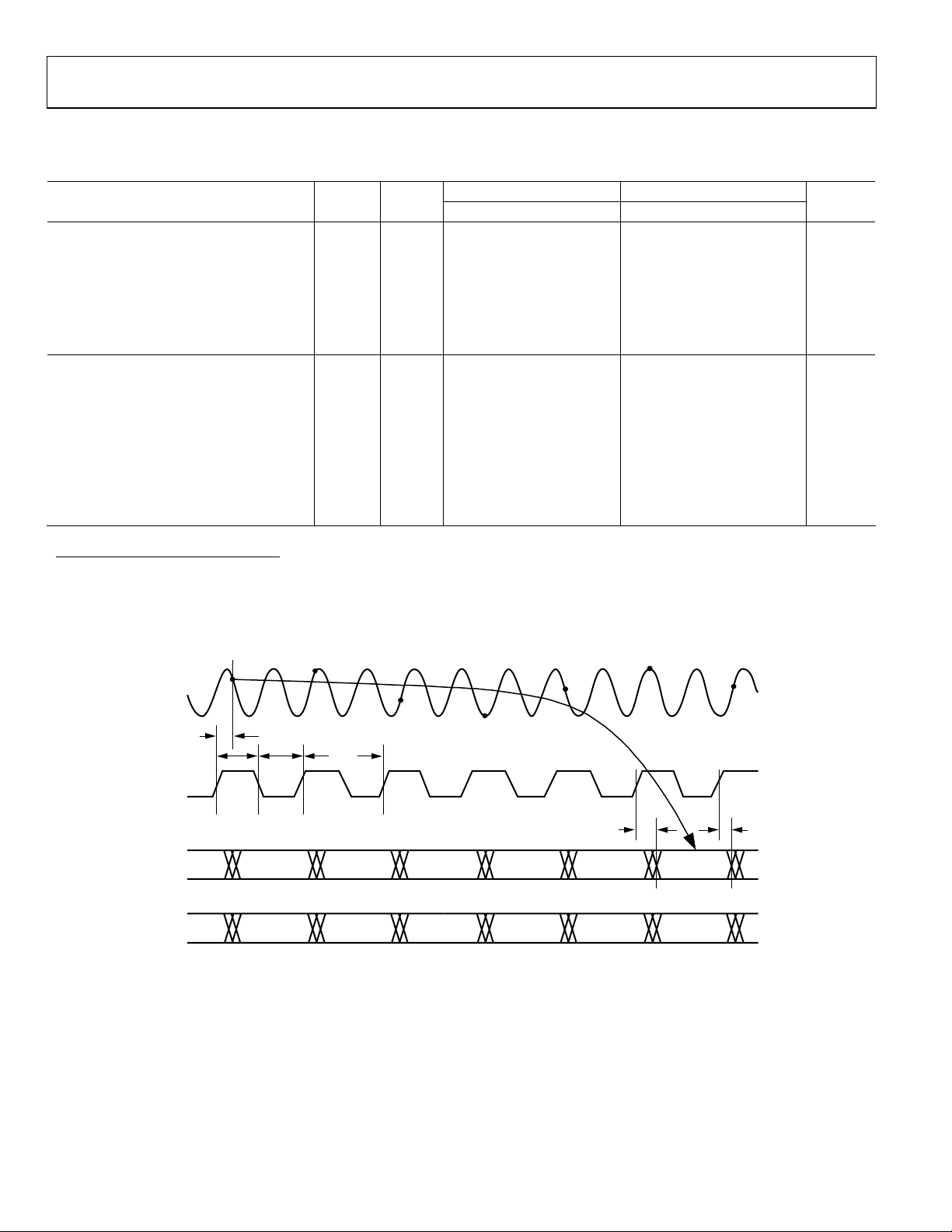
Figure 2. Normal Operation, Same Clock (S1 = 1, S2 = 0) Channel Timing
SAMPLE
N+5
t
PD
SAMPLE
N+6
t
V
02001-B-002
Rev.B | Page 6 of 28

AD9218
AINA
A
ENCODE A
ENCODE B
D9
A
D9B–D0
IN
–D0
SAMPLE
B
t
A
t
EH
A
B
SAMPLE
N
DATA N–10 DATA N–8 DATA N–6 DATA N–4 DATA N–2 DATA N DATA N+2
SAMPLE
N+1
t
N+2
SAMPLE
EL
1/f
DATA N–9 DATA N–7 DATA N–5 DATA N–3 DATA N–1 DATA N+1
N+3
S
SAMPLE
N+4
SAMPLE
N+5
SAMPLE
SAMPLE
N+6
N+7
SAMPLE
N+8
t
PD
t
V
02001-B-003
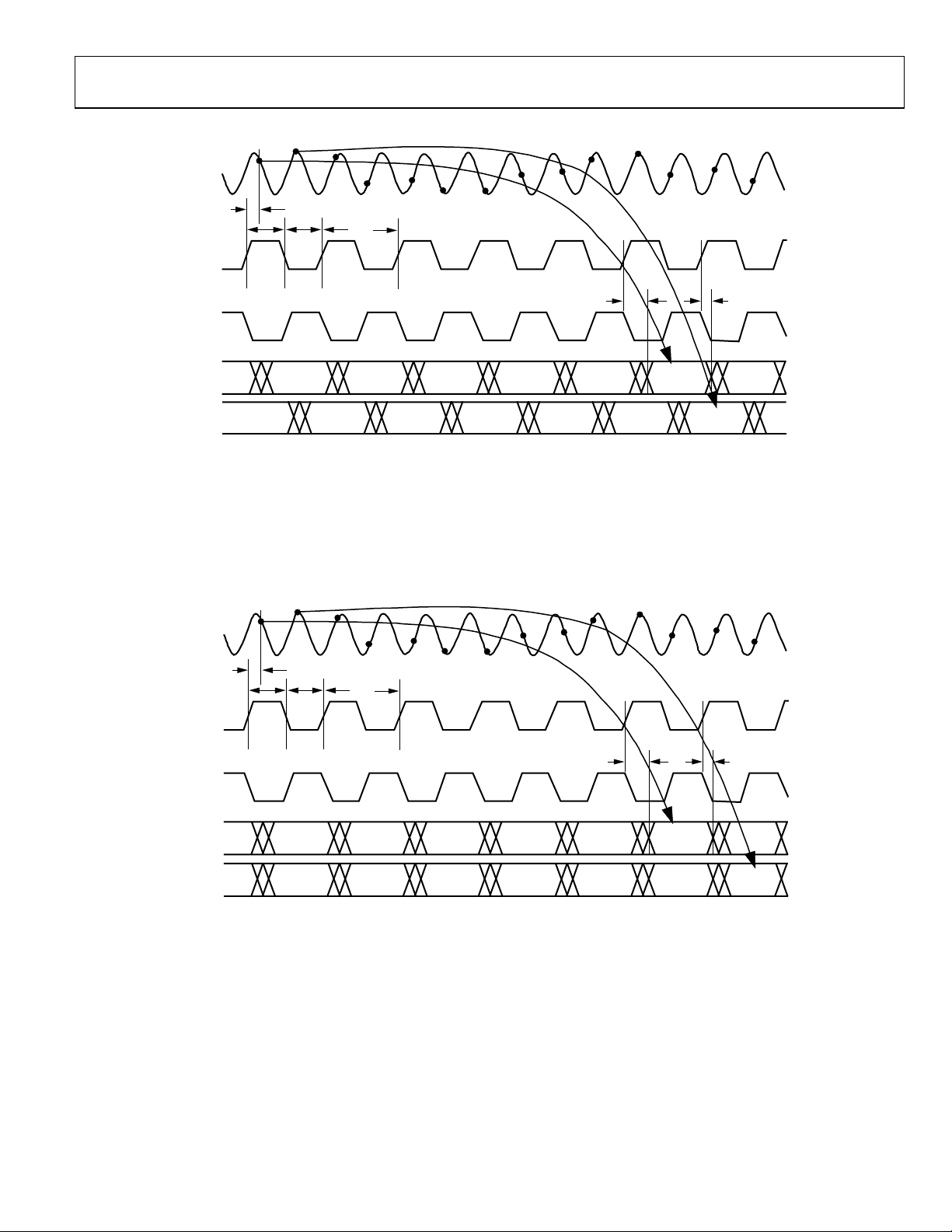
Figure 3. Normal Operation with Two Clock Sources (S1 = 1, S2 = 0) Channel Timing
AINA
A
B
IN
ENCODE A
SAMPLE
t
A
t
EH
SAMPLE
N
N+1
t
SAMPLE
N+2
SAMPLE
EL
1/f
N+3
S
SAMPLE
N+4
SAMPLE
N+5
SAMPLE
SAMPLE
N+6
N+7
SAMPLE
N+8
t
V
02001-B-004
ENCODE B
–D0
D9
A
D9B–D0
t
PD
A
B
DATA N–10 DATA N–8 DATA N–6 DATA N–4 DATA N–2 DATA N DATA N+2
DATA N–11 DATA N–9 DATA N–7 DATA N–5 DATA N–3 DATA N–1 DATA N+1
Figure 4. Data Align with Two Clock Sources (S1 = 1, S2 = 1) Channel Timing
Rev. B | Page 7 of 28

AD9218
ABSOLUTE MAXIMUM RATINGS
Stresses above those listed under Absolute Maximum Ratings
may cause permanent damage to the device. This is a stress
rating only; functional operation of the device at these or any
other conditions outside of those indicated in the operation
sections of this specification is not implied. Exposure to
absolute maximum ratings for extended periods may affect
device reliability.
Table 7. User Select Modes
S1 S2 Power-Down and Data Alignment Settings
0 0 Power down both channel A and B.
0 1 Power down channel B only.
1 0 Normal operation (data align disabled).
1 1
Table 5. Stress Ratings
Parameter Rating
VD, V
DD
Analog inputs –0.5 V to VD + 0.5 V
Digital inputs –0.5 V to VDD + 0.5 V
REFIN inputs –0.5 V to VD + 0.5 V
Digital output current 20 mA
Operating temperature –55°C to +125°C
Storage temperature –65°C to +150°C
Maximum junction temperature 150°C
Maximum case temperature 150°C
θA (measured on a 4-layer board with
solid ground plane)
4 V
57°C/W
Table 6. Test Levels
Test Level Description
I 100% production tested.
II
III Sample tested only.
IV
V Parameter is a typical value only.
VI
100% production tested at 25°C and sample
tested at specified temperatures.
Parameter is guaranteed by design and
characterization testing.
100% production tested at 25°C; guaranteed by
design and characterization testing for industrial
temperature range.
100% production tested at temperature
extremes for military devices.
Data align enabled (data from both channels
available on rising edge of Clock A. Channel B data is
delayed by a 1/2 clock cycle.)
ESD CAUTION
ESD (electrostatic discharge) sensitive device. Electrostatic charges as high as 4000 V readily accumulate on the
human body and test equipment and can discharge without detection. Although this product features
proprietary ESD protection circuitry, permanent damage may occur on devices subjected to high energy
electrostatic discharges. Therefore, proper ESD precautions are recommended to avoid performance
degradation or loss of functionality.
Rev.B | Page 8 of 28

AD9218
PIN CONFIGURATION AND FUNCTION DESCRIPTIONS
(MSB)
A
AD7AD6AD5AD4AD3AD2A
VDENCAVDDGND
4847464544434241403938
1
GND
2
A
A
IN
A
A
3
IN
DFS/GAIN
REF
REF
REF
IN
OUT
IN
A
IN
A
IN
GND
4
A
5
6
B
7
S1
8
9
S2
10
B
11
B
12
1314151617181920212223
D
B
V
ENC
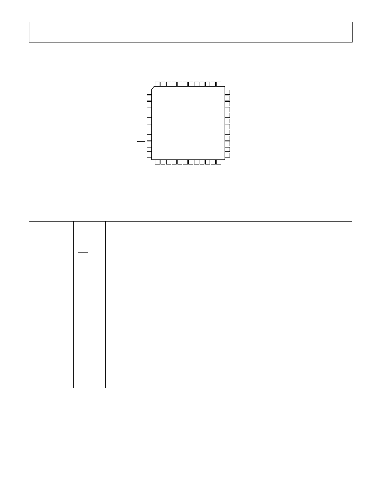
Figure 5. Pin Configuration
D8
D9
AD9218
TOP VIEW
(Not to Scale)
BD8BD7BD6BD5BD4BD3BD2B
DD
V
GND
(MSB) D9
37
36
D1
A
35
D0
A
GND
34
33
V
DD
GND
32
31
V
D
V
30
D
GND
29
28
V
DD
27
GND
26
D0
B
D1
25
B
24
02001-B-005
Table 8. Pin Function Descriptions
Pin Number Mnemonic Description
1, 12, 16, 27, 29,
GND Ground.
32, 34, 45
2 AINA Analog Input for Channel A.
3
AA
IN
4 DFS/GAIN
Analog Input for Channel A (complementary).
Data Format Select and Analog Input Gain Mode. Low = offset binary output available, 1 V p-p supported;
high = twos complement output available, 1 V p-p supported; floating = offset binary output available,
2 V p-p supported; set to V
= twos complement output available, 2 V p-p supported.
REF
5 REFINA Reference Voltage Input for Channel A.
6 REF
Internal Reference Voltage.
OUT
7 REFINB Reference Voltage Input for Channel B.
8 S1 User Select No. 1. Refer to Table 7.
9 S2
10
User Select No. 2. Refer to
BA
IN
Analog Input for Channel B (complementary).
Table 7.
11 AINB Analog Input for Channel B.
13, 30, 31, 48 VD Analog Supply (3 V).
14 ENCB Clock Input for Channel B.
15, 28, 33, 46 VDD Digital Supply (2.5 V to 3.6 V).
17–26 D9B–D0B Digital Output for Channel B (D9B = MSB).
35–44 D0A–D9A Digital Output for Channel A (D9A = MSB).
47 ENCA Clock Input for Channel A.
Rev. B | Page 9 of 28
