ANALOG DEVICES AD9218 Service Manual
查询AD9218供应商查询AD9218供应商
10-Bit, 40/65/80/105 MSPS
a
FEATURES
Dual 10-Bit, 40 MSPS, 65 MSPS, 80 MSPS, and
105 MSPS ADC
Low Power: 275 mW at 105 MSPS per Channel
On-Chip Reference and Track/Holds
300 MHz Analog Bandwidth Each Channel
SNR = 57 dB @ 41 MHz, Encode = 80 MSPS
1 V p-p or 2 V p-p Analog Input Range Each Channel
Single 3.0 V Supply Operation (2.7 V–3.6 V)
Power-Down Mode for Single Channel Operation
Two’s Complement or Offset Binary Output Mode
Output Data Alignment Mode
Pin-Compatible with 8-Bit AD9288
–75 dBc Crosstalk between Channels
APPLICATIONS
Battery-Powered Instruments
Hand-Held Scopemeters
Low Cost Digital Oscilloscopes
I and Q Communications
Ultrasound Equipment
ENCODE A
A
IN
A
IN
REFINA
REF
OUT
REF
IN
AINB
A
IN
ENCODE B
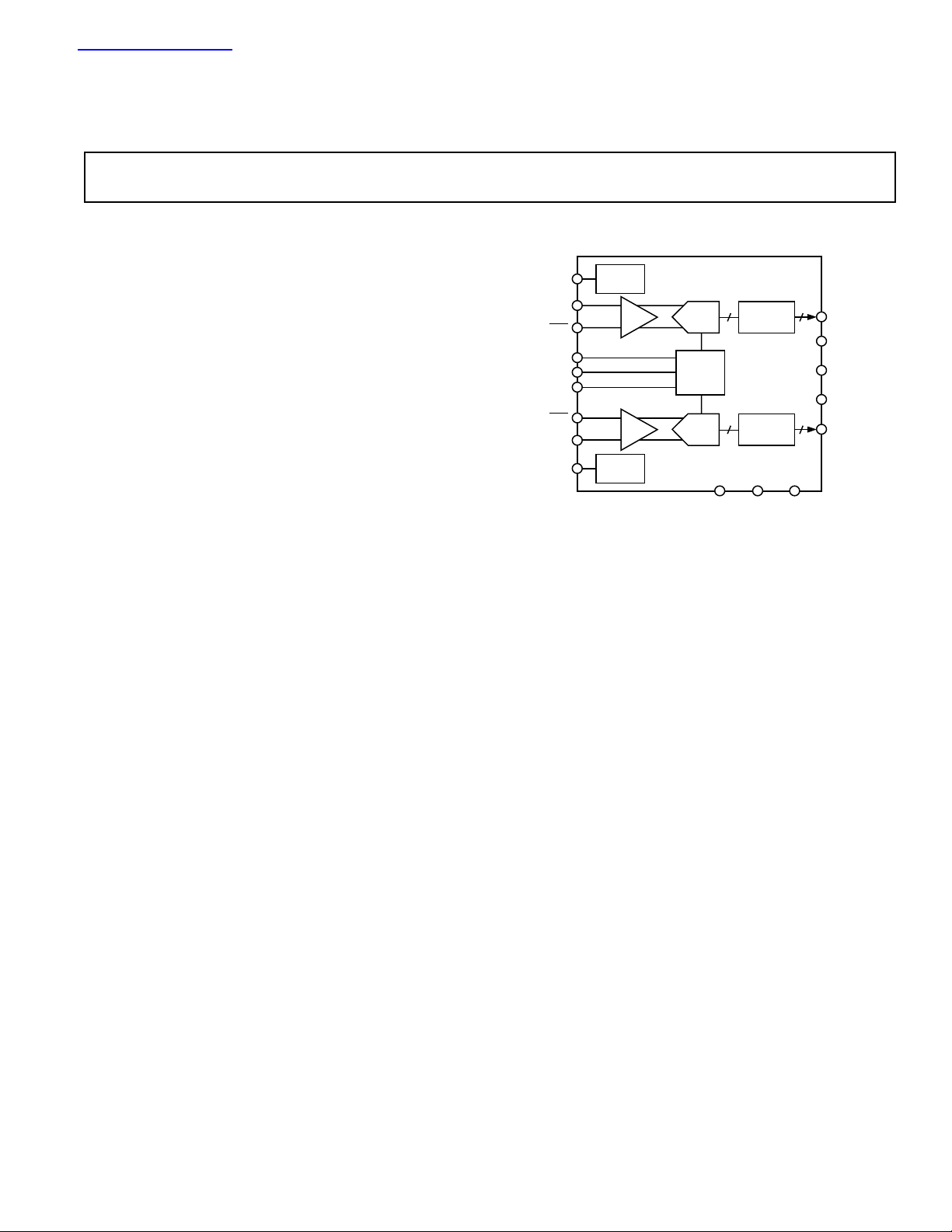
3 V Dual A/D Converter
FUNCTIONAL BLOCK DIAGRAM
FUNCTIONAL BLOCK DIAGRAM
ADC
10 10
REF
ADC
10 10
D
AD9218
OUTPUT
REGISTER
OUTPUT
REGISTER
GNDV
TIMING
A
A
B
B
T/H
T/H
TIMING
AD9218
D9A–D
USER
SELECT #1
USER
SELECT #2
DATA
FORMAT/
GAIN
D
9B–D0B
V
DD
0A
GENERAL DESCRIPTION
The AD9218 is a dual 10-bit monolithic sampling analog-todigital converter with on-chip track-and-hold circuits and is
optimized for low cost, low power, small size and ease of use.
The product operates at a 105 MSPS conversion rate with
outstanding dynamic performance over its full operating range.
Each channel can be operated independently.
The ADC requires only a single 3.0 V (2.7 V to 3.6 V) power
supply and an encode clock for full operation. No external
reference or driver components are required for many applications. The digital outputs are TTL/CMOS-compatible and a
separate output power supply pin supports interfacing with
3.3 V or 2.5 V logic.
The clock input is TTL/CMOS-compatible and the 10-bit
digital outputs can be operated from 3.0 V (2.5 V to 3.6 V)
supplies. User-selectable options are available to offer a combination of power-down modes, digital data formats and digital
data timing schemes. In power-down mode, the digital outputs
are driven to a high-impedance state.
Fabricated on an advanced CMOS process, the AD9218 is
available in a 48-lead surface-mount plastic package (7 × 7 mm
LQFP) specified over the industrial temperature range (–40°C
to +85°C).
PRODUCT HIGHLIGHTS
Low Power—Just 275 mW power dissipation per channel at
105 MSPS. Other speed grade proportionally scaled down while
maintaining high ac performance.
Pin Compatibility Upgrade—Allows easy migration from 8-bit
to 10-bit. Pin-compatible with the 8-bit AD9288 dual ADC.
Ease of Use—On-chip reference and user controls provide flexibility in system design.
High Performance—Maintain 54 dB SNR at 105 MSPS with a
Nyquist input.
Channel Crosstalk—Very low at –75 dBc.
REV. 0
Information furnished by Analog Devices is believed to be accurate and
reliable. However, no responsibility is assumed by Analog Devices for its
use, nor for any infringements of patents or other rights of third parties that
may result from its use. No license is granted by implication or otherwise
under any patent or patent rights of Analog Devices.
One Technology Way, P.O. Box 9106, Norwood, MA 02062-9106, U.S.A.
Tel: 781/329-4700 www.analog.com
Fax: 781/326-8703 © Analog Devices, Inc., 2001

AD9218–SPECIFICATIONS
DC SPECIFICATIONS
(VDD = 3.0 V, VD = 3.0 V; external reference, unless otherwise noted.)
Test AD9218BST-40/-65 AD9218BST-80/-105
Parameter Temp Level Min Typ Max Min Typ Max Unit
RESOLUTION 10 10 Bits
ACCURACY
No Missing Codes
Offset Error
Gain Error
1
2
2
Full VI GNT GNT
25°C I –18 2 18 –18 2 18 LSB
25°C I –2 3 8 –2 3.5 8 % FS
Differential Nonlinearity 25°CI –1 ±0.3/±0.6 1/1.3 –1 ± 0.5/± 0.8 1.2/1.7 LSB
(DNL)
Full VI ±0.8 ±0.6/±0.9 LSB
Integral Nonlinearity (INL) 25°C I –1/–1.6 ±0.3/±1 1/1.6 –1.35/–2.7 ±0.75/±2 1.35/2.7 LSB
Full VI ±1 ±1/±2.3 LSB
TEMPERATURE DRIFT
Offset Error Full V 10 4 ppm/°C
Gain Error
2
Full V 80 100 ppm/°C
Reference Full V 40 40 ppm/°C
REFERENCE
Internal Reference Voltage 25°C I 1.18 1.24 1.28 1.18 1.24 1.28 V
(REFOUT)
Input Resistance (REFIN A, B) Full V 9 11 13 9 11 13 kΩ
ANALOG INPUTS
Differential Input Voltage Full V 1 or 2 1 V
Range (AIN, AIN)
3
Common-Mode Voltage Full V VD/3 VD/3 V
Input Resistance Full VI 8 10 14 8 10 14 kΩ
Input Capacitance 25°CV 3 3 pF
POWER SUPPLY
V
D
V
DD
Supply Currents
IV
(VD = 3.0 V)
D
(VDD = 3.0 V)
IV
DD
4
4
Power Dissipation DC
IV
Power-Down Current
D
5
6
Full IV 2.7 3 3.6 2.7 3 3.6 V
Full IV 2.7 3 3.6 2.7 3 3.6 V
Full VI 108/117 113/122 172/183 175/188 mA
25°C V 7/11 13/17 mA
Full VI 325/350 340/365 515/550 525/565 mW
Full VI 20 22 mA
Power Supply Rejection Ratio 25°CI ±1 ±1 mV/V
NOTES
1
No Missing Codes across industrial temperature range guaranteed for -40 MSPS, -65 MSPS, and -80 MSPS grades. No missing codes at room temperature guaranteed for -105 grade.
2
Gain error and gain temperature coefficients are based on the ADC only (with a fixed 1.25 V external reference) -65 Grade in 2 V p-p range, -40, -85, -105 Grades in
1 V p-p range.
3
(AIN – AIN) = ±0.5 V in 1 V range (full scale), (AIN – AIN) = ± 1 V in 2 V range (full scale).
4
AC Power Dissipation measured with rated encode and a 10.3 MHz analog input @ 0.5 dBFS, C
5
DC Power Dissipation measured with rated encode and a dc analog input (Outputs Static, IVDD = 0)
6
In power-down state IVDD = ±10 µA typical (all grades).
Specifications subject to change without notice.
LOAD
= 5 pF.
–2–
REV. 0

AD9218
DIGITAL SPECIFICATIONS
(VDD = 3.0 V, VD = 3.0 V; external reference, unless otherwise noted.)
Test AD9218BST-40/-65 AD9218BST-80/-105
Parameter Temp Level Min Typ Max Min Typ Max Unit
DIGITAL INPUTS
Encode Input Common Mode Full V VD/2 VD/2 V
Encode “1” Voltage Full VI 2 2 V
Encode “0” Voltage Full VI 0.8 0.8 V
Encode Input Resistance Full VI 1.8 2.0 2.3 1.8 2.0 2.3 kΩ
Logic “1” Voltage—S1, S2, DFS Full VI 2 2 V
Logic “0” Voltage—S1, S2, DFS Full VI 0.8 0.8 V
Logic “1” Current—S1 Full VI –50 ±10 +50 –50 ±10 +50 µA
Logic “0” Current—S1 Full VI –400 –230 –50 –400 –230 –50 µA
Logic “1” Current—S2 Full VI 50 230 400 50 230 400 µA
Logic “0” Current—S2 Full VI –50 ±10 +50 –50 ±10 +50 µA
Logic “1” Current—DFS Full VI 30 100 200 30 100 200 µA
Logic “0” Current—DFS Full VI –400 –230 –50 –400 –230 –50 µA
Input Capacitance—S1, S2, Encode Inputs 25°CV 2 2 pF
Input Capacitance DFS 25°C V 4.5 4.5 pF
DIGITAL OUTPUTS
Logic “1” Voltage Full VI 2.45 2.45 V
Logic “0” Voltage Full VI 0.05 0.05 V
Output Coding Two’s Comp. or Offset Binary Two’s Comp. or Offset Binary
Specifications subject to change without notice.
AC SPECIFICATIONS
(V
= 3.0 V, VD = 3.0 V; external reference, unless otherwise noted.)
DD
Test AD9218BST-40/-65 AD9218BST-80/-105
Parameter Temp Level Min Typ Max Min Typ Max Unit
DYNAMIC PERFORMANCE
1
Signal-to-Noise Ratio (SNR)
(Without Harmonics)
fIN = 10.3 MHz 25°C I 58/55 59/57 57/53 58/55 dB
f
= Nyquist
IN
2
25°C I -/54 59/56 55/52 57/54 dB
Signal-to-Noise Ratio (SINAD)
(With Harmonics)
f
= 10.3 MHz 25°C I 58/54 59/56 56/52 58/53 dB
IN
f
= Nyquist
IN
2
25°C I -/53 59/55 55/51 57/53 dB
Effective Number of Bits
fIN = 10.3 MHz 25°C I 9.4/8.8 9.6/9.1 9.1/8.4 9.4/8.6 Bits
f
= Nyquist
IN
2
25°C I -/8.6 9.6/8.9 9/8.3 9.3/8.6 Bits
Second Harmonic Distortion
fIN = 10.3 MHz 25°C I –72/–66 –89/–77 –69/–60 –77/–68 dBc
f
= Nyquist
IN
2
25°C I -/–63 –89/–72 –65/–57 –76/–66 dBc
Third Harmonic Distortion
fIN = 10.3 MHz 25°C I –68/–62 –79/–68 –62/–57 –71/–63 dBc
f
= Nyquist
IN
2
25°C I -/–60 –78/–64 –63/–57 –73/–69 dBc
Spurious Free Dynamic Range SFDR
fIN = 10.3 MHz 25°C I –68/–62 –79/–67 –62/–57 –69/–62 dBc
f
= Nyquist
IN
2
25°C I -/–60 –78/–64 –63/–57 –70/–63 dBc
Two-Tone Intermod Distortion (IMD)
f
= 10 MHz, f
IN1
= 11 MHz 25°C V –74/–73 dBc
IN2
at –7 dBFS
f
= 30 MHz, f
IN1
= 31 MHz 25°C V –73/–73 –77/–67 dBc
IN2
at –7 dBFS
Analog Bandwidth, Full Power 25°C V 300 300 MHz
Crosstalk 25°C V –75 –75 dBc
NOTES
1
AC specs based on an analog input voltage of –0.5 dBFS at 10.3 MHz unless otherwise noted. AC specs for -40, -80, -105 grades are tested in 1 V p-p range and
driven differentially. AC specs for -65 grade are tested in 2 V p-p range and driven differentially.
2
The -65, -80, and -105 grades are tested close to Nyquist for that grade: 31 MHz, 39 MHz, and 51 MHz for the -65, -80, and -105 grades respectively.
Specifications subject to change without notice.
REV. 0
–3–
AD9218–SPECIFICATIONS
SWITCHING SPECIFICATIONS
(VDD = 3.0 V, VD = 3.0 V; external reference, unless otherwise noted.)
Test AD9218BST-40/-65 AD9218BST-80/-105
Parameter Temp Level Min Typ Max Min Typ Max Unit
ENCODE INPUT PARAMETERS
Maximum Encode Rate Full VI 40/65 80/105 MSPS
Minimum Encode Rate Full IV 20/20 20/20 MSPS
Encode Pulsewidth High (t
Encode Pulsewidth Low (t
Aperture Delay (t
)25°CV 2 2 ns
A
) Full IV 7/6 5/3.8 ns
EH
) Full IV 7/6 5/3.8 ns
EL
Aperture Uncertainty (Jitter) 25°C V 3 3 ps rms
DIGITAL OUTPUT PARAMETERS
Output Valid Time (tV)* Full VI 3 3 ns
Output Propagation Delay (t
Output Rise Time (t
Output Fall Time (t
)25°C V 1 1.0 ns
R
)25°C V 1.2 1.2 ns
F
)* Full VI 4.5 7 4.5 6 ns
PD
Out of Range Recovery Time 25°CV 5 5 ns
Transient Response Time 25°CV 5 5 ns
Recovery Time from Power-Down 25°C V 10 10 Cycles
Pipeline Delay Full IV 5 5 Cycles
NOTES
*tV and tPD are measured from the 1.5 level of the ENCODE input to the 50%/50% levels of the digital outputs swing. The digital output load during test is not to
exceed an ac load of 5 pF or a dc current of ± 40 µA. Rise and fall times measured from 10% to 90%.
Specifications subject to change without notice.
SAMPLE N
SAMPLE
N+1
SAMPLE
N+5
SAMPLE
N+6
ENCODE
A&B
D9A–D
D9B–D
A,
A
IN
B
A
IN
t
A
t
EH
0A
0B
t
EL
DATA N–5
DATA N–5 DATA N–4 DATA N–3 DATA N–2 DATA N–1 DATA N
1/f
DATA N–4 DATA N–3 DATA N–2 DATA N–1 DATA N
SAMPLE
N+2
S
SAMPLE
N+3
SAMPLE
N+4
t
PD
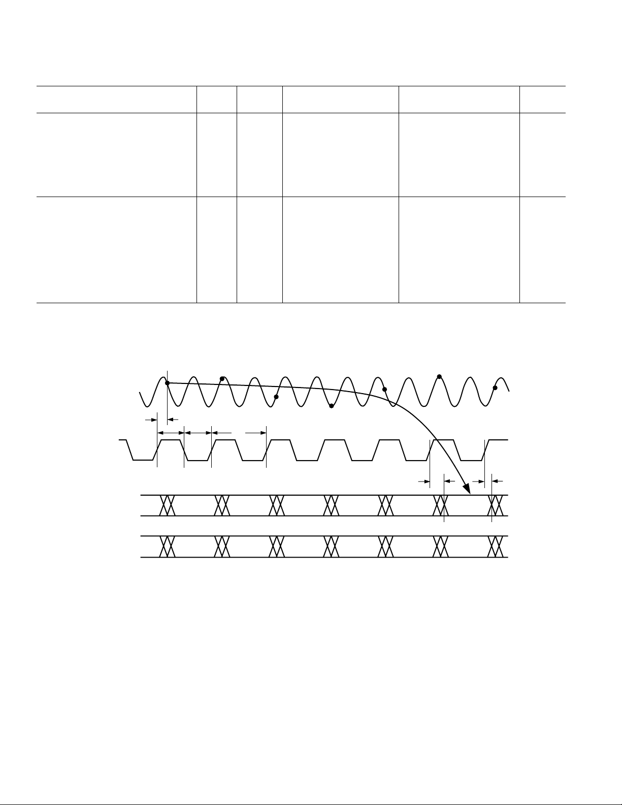
Figure 1. Normal Operation, Same Clock (S1 = 1, S2 = 0) Channel Timing
t
V
–4–
REV. 0
AD9218
SAMPLE
N+1
t
N+2
SAMPLE
EL
DATA N–9 DATA N–7 DATA N–5 DATA N–3 DATA N–1 DATA N+1
SAMPLE
N+3
1/f
S
N+4
SAMPLE
N+5
SAMPLE
SAMPLE
N+6
N+7
SAMPLE
N+8
t
PD
ENCODE A
ENCODE B
D
D9B–D
A
A,
IN
A
IN
9A–D0A
SAMPLE
B
t
A
t
EH
0B
SAMPLE
N
DATA N–10 DATA N–8 DATA N–6 DATA N–4 DATA N–2 DATA N DATA N+2
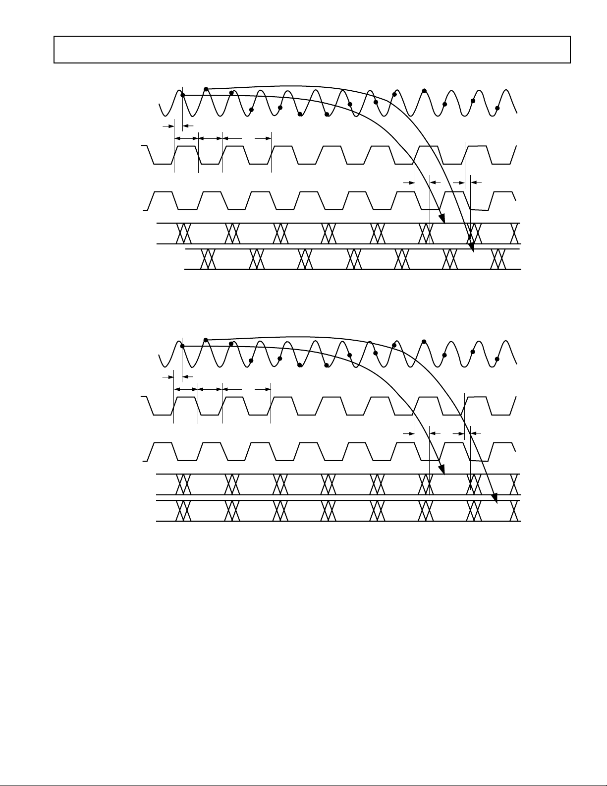
Figure 2. Normal Operation with Two Clock Sources (S1 = 1, S2 = 0) Channel Timing
SAMPLE
N+1
t
EL
SAMPLE
N+2
SAMPLE
1/f
N+3
S
SAMPLE
N+4
SAMPLE
N+5
SAMPLE
SAMPLE
N+6
N+7
SAMPLE
N+8
ENCODE A
SAMPLE
N
A
A,
IN
A
B
IN
t
A
t
EH
t
V
ENCODE B
D
D9B–D
t
PD
9A–D0A
0B
DATA N–10 DATA N–8 DATA N–6 DATA N–4 DATA N–2 DATA N DATA N+2
DATA N–11 DATA N–9 DATA N–7 DATA N–5 DATA N–3 DATA N–1 DATA N+1
Figure 3. Data Align with Two Clock Sources (S1 = 1, S2 = 1) Channel Timing
t
V
REV. 0
–5–
AD9218
WARNING!
ESD SENSITIVE DEVICE
ABSOLUTE MAXIMUM RATINGS
VD, VDD . . . . . . . . . . . . . . . . . . . . . . . . . . . . . . . . . . . . . . . 4 V
Analog Inputs . . . . . . . . . . . . . . . . . . . . –0.5 V to V
Digital Inputs . . . . . . . . . . . . . . . . . . . –0.5 V to V
REF
Inputs . . . . . . . . . . . . . . . . . . . . . –0.5 V to VD + 0.5 V
IN
Digital Output Current . . . . . . . . . . . . . . . . . . . . . . . . . 20 mA
Operating Temperature . . . . . . . . . . . . . . . . –55°C to +125°C
Storage Temperature . . . . . . . . . . . . . . . . . . –65°C to +150°C
Maximum Junction Temperature . . . . . . . . . . . . . . . . . 150°C
Maximum Case Temperature . . . . . . . . . . . . . . . . . . . . 150°C
2
. . . . . . . . . . . . . . . . . . . . . . . . . . . . . . . . . . . . . . . 57°C/W
θ
JA
NOTES
1
Stresses above those listed under Absolute Maximum Ratings may cause permanent damage to the device. This is a stress rating only; functional operation of the
device at these or any other conditions outside of those indicated in the operation
sections of this specification is not implied. Exposure to absolute maximum ratings
for extended periods may affect device reliability.
2
Measured on a four-layer board with solid ground plane.
1
EXPLANATION OF TEST LEVELS
Test Level
+ 0.5 V
D
+ 0.5 V
DD
I 100% production tested.
II 100% production tested at 25°C and sample tested at speci-
fied temperatures.
III Sample tested only.
IV Parameter is guaranteed by design and characterization testing.
V Parameter is a typical value only.
VI 100% production tested at 25°C; guaranteed by design
and characterization testing for industrial temperature
range; 100% production tested at temperature extremes
for military devices.
CAUTION
ESD (electrostatic discharge) sensitive device. Electrostatic charges as high as 4000 V readily
accumulate on the human body and test equipment and can discharge without detection. Although
the AD9218 features proprietary ESD protection circuitry, permanent damage may occur on
devices subjected to high-energy electrostatic discharges. Therefore, proper ESD precautions are
recommended to avoid performance degradation or loss of functionality.
ORDERING GUIDE
Temperature Package
Model Range Package Description Option
AD9218BST-40, -65, -80, -105 –40°C to +85°C Metric Quad Flat Pack (1.4 mm thick: LQFP) ST-48
AD9218-65PCB 25°C Evaluation Board (Supports -40/-65 Grade)
AD9218-105PCB 25°C Evaluation Board (Supports -80/-105 Grade)
Table I. User Select Modes
S1 S2 User Select Options
0 0 Power-Down Both Channel A and B.
0 1 Power-Down Channel B Only.
1 0 Normal Operation (Data Align Disabled).
1 1 Data Align Enabled (data from both channels
available on rising edge of Clock A. Channel B
data is delayed by a 1/2 clock cycle.)
–6–
REV. 0
AD9218
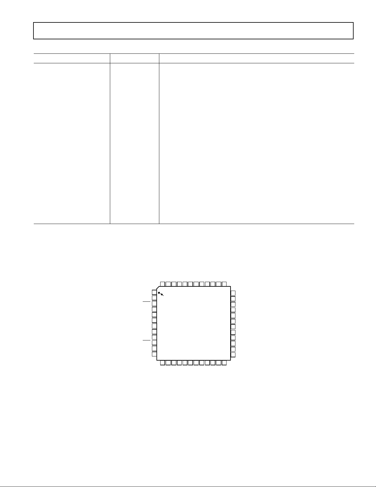
PIN FUNCTION DESCRIPTIONS
Pin No. Mnemonic Description
1, 12, 16, 27, 29, 32, 34, 45 GND Ground
2A
3 AINA Analog Input for Channel A (Complementary)
4 DFS/GAIN Data Format Select and Analog Input Gain Mode. (Low = offset binary out-
5 REF
6 REF
7 REFINB Reference Voltage Input for Channel B
8 S1 User Select #1 (Refer to Table I)
9 S2 User Select #2 (Refer to Table I)
10 AINB Analog Input for Channel B (Complementary)
11 A
13, 30, 31, 48 V
14 ENC
15, 28, 33, 46 V
17–26 D9
35–44 D0
47 ENC
A Analog Input for Channel A
IN
put available, 1 V p-p supported; high = two’s complement output available,
1 V p-p supported; floating = offset binary output available, 2 V p-p supported;
Set to V
A Reference Voltage Input for Channel A
IN
OUT
B Analog Input for Channel B
IN
D
B
DD
–D0
B
B
–D9
A
A
A
Internal Reference Voltage
Analog Supply (3 V)
Clock Input for Channel B
Digital Supply (2.5 V to 3.6 V)
Digital Output for Channel B (D9B = MSB)
Digital Output for Channel A (D9A = MSB)
Clock Input for Channel A
= two’s complement output available, 2 V p-p supported.)
REF
GND
A
IN
AINA
DFS/GAIN
REF
IN
REF
OUT
REFINB
A
IN
AINB
GND
PIN CONFIGURATION
(MSB)
B
ENC
V
A
D9
AD9218
TOP VIEW
(Not to Scale)
B
DD
GND
(MSB) D9
VDENCAVDDGND
48 47 46 45 44 39 38 3743 42 41 40
1
PIN 1
2
A
IDENTIFIER
3
4
5
A
6
7
8
S1
9
S2
B
10
11
12
13 14 15 16 17 18 19 20 21 22 23 24
D
V
AD7AD6AD5AD4AD3AD2A
D8
D8BD7BD6BD5BD4BD3BD2
36
D1
A
35
D0
A
34
GND
33
V
DD
32
GND
31
V
D
30
V
D
29
GND
28
V
DD
27
GND
26
D0
B
25
D1
B
B
REV. 0
–7–

AD9218
TERMINOLOGY
Analog Bandwidth
The analog input frequency at which the spectral power of the
fundamental frequency (as determined by the FFT analysis) is
reduced by 3 dB.
Aperture Delay
The delay between the 50% point of the rising edge of the
ENCODE command and the instant at which the analog input
is sampled.
Aperture Uncertainty (Jitter)
The sample-to-sample variation in aperture delay.
Crosstalk
Coupling onto one channel being driven by a low level (–40 dBFS)
signal when the adjacent interfering channel is driven by a
full-scale signal.
Differential Analog Input Resistance, Differential Analog
Input Capacitance and Differential Analog Input Impedance
The real and complex impedances measured at each analog
input port. The resistance is measured statically and the capacitance and differential input impedances are measured with a
network analyzer.
Differential Analog Input Voltage Range
The peak-to-peak differential voltage that must be applied to
the converter to generate a full-scale response. Peak differential
voltage is computed by observing the voltage on a single pin
and subtracting the voltage from the other pin, which is 180
degrees out of phase. Peak-to-peak differential is computed by
rotating the inputs phase 180 degrees and again taking the peak
measurement. The difference is then computed between both
peak measurements.
Differential Nonlinearity
The deviation of any code width from an ideal 1 LSB step.
Effective Number of Bits
The effective number of bits (ENOB) is calculated from the
measured SNR based on the equation:
SNR dB
ENOB
ENCODE Pulsewidth/Duty Cycle
MEASURED
=
– ..176
602
Pulsewidth high is the minimum amount of time that the
ENCODE pulse should be left in Logic 1 state to achieve rated
performance; pulsewidth low is the minimum time ENCODE
pulse should be left in low state. See timing implications of
changing t
in text. At a given clock rate, these specifica-
ENCH
tions define an acceptable ENCODE duty cycle.
Full-Scale Input Power
Expressed in dBm. Computed using the following equation:
Gain Error
Power
Full Scale
−
2
V
Full Scale rms
Z
10
=
log
INPUT
0 001
.
−
Gain error is the difference between the measured and ideal full
scale input voltage range of the ADC.
Harmonic Distortion, Second
The ratio of the rms signal amplitude to the rms value of the
second harmonic component, reported in dBc.
Harmonic Distortion, Third
The ratio of the rms signal amplitude to the rms value of the
third harmonic component, reported in dBc.
Integral Nonlinearity
The deviation of the transfer function from a reference line
measured in fractions of 1 LSB using a “best straight line”
determined by a least square curve fit.
Minimum Conversion Rate
The encode rate at which the SNR of the lowest analog signal
frequency drops by no more than 3 dB below the guaranteed limit.
Maximum Conversion Rate
The encode rate at which parametric testing is performed.
Output Propagation Delay
The delay between a differential crossing of ENCODE and
ENCODE and the time when all output data bits are within
valid logic levels.
Noise (for Any Range within the ADC)
VZ
=× ×
NOISE
0 001 10
.
−−
FS SNR Signal
dBm dBc dBFS
10
Where Z is the input impedance, FS is the full scale of the
device for the frequency in question, SNR is the value for the
particular input level, and Signal is the signal level within the
ADC reported in dB below full scale. This value includes both
thermal and quantization noise.
Power Supply Rejection Ratio
The ratio of a change in input offset voltage to a change in
power supply voltage.
Signal-to-Noise-and-Distortion (SINAD)
The ratio of the rms signal amplitude (set 1 dB below full scale)
to the rms value of the sum of all other spectral components,
including harmonics but excluding dc.
Signal-to-Noise Ratio (without Harmonics)
The ratio of the rms signal amplitude (set at 1 dB below full
scale) to the rms value of the sum of all other spectral components, excluding the first five harmonics and dc.
Spurious-Free Dynamic Range (SFDR)
The ratio of the rms signal amplitude to the rms value of the
peak spurious spectral component. The peak spurious component may or may not be a harmonic. May be reported in dBc
(i.e., degrades as signal level is lowered), or dBFS (always
related back to converter full scale).
Two-Tone Intermodulation Distortion Rejection
The ratio of the rms value of either input tone to the rms value
of the worst third order intermodulation product; reported in dBc.
Two-Tone SFDR
The ratio of the rms value of either input tone to the rms value
of the peak spurious component. The peak spurious component
may or may not be an IMD product. May be reported in dBc
(i.e., degrades as signal level is lowered), or in dBFS (always
related back to converter full scale).
–8–
REV. 0
 Loading...