Analog Devices AD9215 a Datasheet

10-Bit, 65/80/105 MSPS,
FEATURES
Single 3 V supply operation (2.7 V to 3.3 V)
SNR = 58 dBc (to Nyquist)
SFDR = 77 dBc (to Nyquist)
Low power ADC core: 96 mW at 65 MSPS, 104 mW
@ 80 MSPS, 120 mW at 105 MSPS
Differential input with 300 MHz bandwidth
On-chip reference and sample-and-hold amplifier
DNL = ±0.25 LSB
Flexible analog input: 1 V p-p to 2 V p-p range
Offset binary or twos complement data format
Clock duty cycle stabilizer
APPLICATIONS
Ultrasound equipment
IF sampling in communications receivers
Battery-powered instruments
Hand-held scopemeters
Low cost digital oscilloscopes
VIN+
VIN–
REFT
REFB
VREF
SENSE
3 V A/D Converter
FUNCTIONAL BLOCK DIAGRAM
DRVDD
10
MODE
SELECT
REF
SELECT
AVDD
SHA
AD9215
AGND
PIPELINE
ADC CORE
CORRECTION LOGIC
OUTPUT BUFFERS
CLOCK
DUTY CYCLE
STABLIZER
0.5V
CLK PDWN MODE
Figure 1.
AD9215
OR
D9 (MSB)
D0
DGND
02874-A-001
PRODUCT DESCRIPTION
The AD9215 is a family of monolithic, single 3 V supply, 10-bit,
65/80/105 MSPS analog-to-digital converters (ADC). This family
features a high performance sample-and-hold amplifier (SHA)
and voltage reference. The AD9215 uses a multistage differential
pipelined architecture with output error correction logic to provide 10-bit accuracy at 105 MSPS data rates and to guarantee no
missing codes over the full operating temperature range.
The wide bandwidth, truly differential sample-and-hold amplifier (SHA) allows for a variety of user-selectable input ranges
and offsets including single-ended applications. It is suitable for
multiplexed systems that switch full-scale voltage levels in
successive channels and for sampling single-channel inputs at
frequencies well beyond the Nyquist rate. Combined with
power and cost savings over previously available ADCs, the
AD9215 is suitable for applications in communications, imaging, and medical ultrasound.
A single-ended clock input is used to control all internal conversion
cycles. A duty cycle stabilizer compensates for wide variations in the
clock duty cycle while maintaining excellent performance. The digital
output data is presented in straight binary or twos complement formats. An out-of-range signal indicates an overflow condition, which
can be used with the MSB to determine low or high overflow.
Fabricated on an advanced CMOS process, the AD9215 is available in both a 28-lead surface-mount plastic package and a
32-lead chip scale package and is specified over the industrial
temperature range of −40°C to +85°C.
PRODUCT HIGHLIGHTS
1. The AD9215 operates from a single 3 V power supply and
features a separate digital output driver supply to accommodate 2.5 V and 3.3 V logic families.
2. Operating at 105 MSPS, the AD9215 core ADC consumes
a low 120 mW; at 80 MSPS, the power dissipation is 104
mW; and at 65 MSPS, the power dissipation is 96 mW.
3. The patented SHA input maintains excellent performance
for input frequencies up to 200 MHz and can be configured for single-ended or differential operation.
4. The AD9215 is part of several pin compatible 10-, 12-, and
14-bit low power ADCs. This allows a simplified upgrade
from 10 bits to 12 bits for systems up to 80 MSPS.
5. The clock duty cycle stabilizer maintains converter per-
formance over a wide range of clock pulse widths.
6. The out of range (OR) output bit indicates when the signal
is beyond the selected input range.
Rev. A
Information furnished by Analog Devices is believed to be accurate and reliable.
However, no responsibility is assumed by Analog Devices for its use, nor for any
infringements of patents or other rights of third parties that may result from its use.
Specifications subject to change without notice. No license is granted by implication
or otherwise under any patent or patent rights of Analog Devices. Trademarks and
registered trademarks are the property of their respective owners.
One Technology Way, P.O. Box 9106, Norwood, MA 02062-9106, U.S.A.
Tel: 781.329.4700
Fax: 781.326.8703 © 2004 Analog Devices, Inc. All rights reserved.
www.analog.com

AD9215
TABLE OF CONTENTS
Specifications..................................................................................... 3
REVISION HISTORY
Absolute Maximum Ratings............................................................ 6
Explanation of Test Levels........................................................... 6
ESD Caution.................................................................................. 6
Pin Configurations and Function Descriptions ........................... 7
Equivalent Circuits....................................................................... 8
Definitions of Specifications ....................................................... 8
Typical Performance Characteristics ........................................... 10
Applying the AD9215 Theory of Operation............................... 14
Clock Input and Considerations ..............................................15
Evaluation Board ........................................................................ 18
Outline Dimensions ....................................................................... 33
Ordering Guide........................................................................... 34
2/04—Data Sheet Changed from a REV. 0 to a REV. A
Renumbered Figures and Tables ..............................UNIVERSAL
Changes to Product Title................................................................ 1
Changes to Features ........................................................................ 1
Changes to Product Description................................................... 1
Changes to Product Highlights .....................................................1
Changes to Specifications............................................................... 2
Changes to Figure 2......................................................................... 4
Changes to Figures 9 to 11 ........................................................... 10
Added Figure 14 ............................................................................10
Added Figures 16 and 18.............................................................. 11
Changes to Figures 21 to 24 and 25 to 26................................... 12
Deleted Figure 25........................................................................... 12
Changes to Figures 28 and 29...................................................... 13
Changes to Figure 31.....................................................................14
Changes t0 Figure 35..................................................................... 16
Changes to Figures 50 through 58...............................................26
Added Table 11 .............................................................................. 31
Updated Outline Dimensions...................................................... 32
Changes to Ordering Guide......................................................... 33
5/03—Revision 0: Initial Version
Rev. A | Page 2 of 36

AD9215
SPECIFICATIONS
AVDD = 3 V, DRVDD = 2.5 V, specified maximum conversion rate, 2 V p-p differential input, 1.0 V internal reference, unless otherwise
noted.
Table 1. DC Specifications
AD9215BRU-65/
AD9215BCP-65
Parameter
Temp
Test
Level Min Typ Max Min Typ Max Min Typ Max Unit
RESOLUTION Full VI 10 10 10 Bits
ACCURACY
No Missing Codes Full VI Guaranteed Guaranteed Guaranteed
Offset Error1 Full VI ±0.3 ±2.0 ±0.3 ±2.0 ±0.3 ±2.0 % FSR
Gain Error1 Full VI 0 +1.5 +4.0 +1.5 +4.0 +1.5 +4.0 % FSR
Differential Nonlinearity (DNL)2 Full VI −1.0 ±0.5 +1.0 −1.0 ±0.5 +1.0 −1.0 ±0.6 +1.2 LSB
Integral Nonlinearity (INL)2 Full VI ±0.5 ±1.2 ±0.5 ±1.2 ±0.65 ±1.2 LSB
TEMPERATURE DRIFT
Offset Error1 Full V +15 +15 +15 ppm/°C
Gain Error
1
Full V +30 +30 +30 ppm/°C
Reference Voltage (1 V Mode) Full V ±230 ±230 ±230 ppm/°C
INTERNAL VOLTAGE REFERENCE
Output Voltage Error (1 V Mode) Full VI ±2 ±35 ±2 ±35 ±2 ±35 mV
Load Regulation @ 1.0 mA Full V 0.2 0.2 0.2 mV
Output Voltage Error (0.5 V Mode) Full V ± 1 ±1 ±1 mV
Load Regulation @ 0.5 mA Full V 0.2 0.2 0.2 mV
INPUT REFERRED NOISE
VREF = 0.5 V 25°C V 0.8 0.8 0.8 LSB rms
VREF = 1.0 V 25°C V 0.4 0.4 0.4 LSB rms
ANALOG INPUT
Input Span, VREF = 0.5 V Full IV 1 1 1 V p-p
Input Span, VREF = 1.0 V Full IV 2 2 2 V p-p
Input Capacitance3 Full V 2 2 2 pF
REFERENCE INPUT RESISTANCE Full V 7 7 7 kΩ
POWER SUPPLIES
Supply Voltage
AVDD Full IV 2.7 3.0 3.3 2.7 3.0 3.3 2.7 3.0 3.3 V
DRVDD Full IV 2.25 2.5 3.6 2.25 2.5 3.6 2.25 2.5 3.6 V
Supply Current
2
I
Full VI 32 35 34.5 39 40 44 mA
AVDD
2
I
25°C V 7.0 8.6 11.3 mA
DRVDD
PSRR Full V ± 0.1 ± 0.1 ± 0.1 % FSR
POWER CONSUMPTION
Sine Wave Input2
2
I
Full VI 96 104 120 mW
AVDD
2
I
25°C V 18 20 25 mW
DRVDD
Standby Power4 25°C V 1.0 1.0 1.0 mW
AD9215BRU-80/
AD9215BCP-80
AD9215BRU-105/
AD9215BCP-105
1
With a 1.0 V internal reference.
2
Measured at fIN = 2.4 MHz, full-scale sine wave, with approximately 5 pF loading on each output bit.
3
Input capacitance refers to the effective capacitance between one differential input pin and AGND. Refer to for the equivalent analog input structure. Figure 5
4
Standby power is measured with a dc input, the CLK pin inactive (i.e., set to AVDD or AGND).
Rev. A | Page 3 of 36

AD9215
AVDD = 3 V, DRVDD = 2.5 V, specified maximum conversion rate, 2 V p-p differential input, 1.0 V internal reference,
AIN = −0.5 dBFS, MODE = AVDD/3 (duty cycle stabilizer [DCS] enabled), unless otherwise noted.
Table 2. AC Specifications
AD9215BRU-65/
AD9215BCP-65
Parameter
Temp
Test
Level
Min Typ Max Min Typ Max Min Typ Max Unit
SIGNAL-TO-NOISE RATIO (SNR)
fIN = 2.4 MHz Full VI 56.0 58.5 56.0 58.5 57.5 dB
25°C I 57.0 59.0 57.0 59.0 56.6 58.5 dB
fIN = Nyquist
1
Full VI 56.0 58.0 56.0 58.0 57.5 dB
25°C I 56.5 58.5 56.5 58.5 56.4 58.0 dB
fIN = 70 MHz 25°C V 58.0 57.8 dB
fIN = 100 MHz 25°C V 57.5 57.7 dB
SIGNAL-TO-NOISE AND DISTORTION (SINAD)
fIN = 2.4 MHz Full VI 55.8 58.5 55.7 58.5 57.6 dB
25°C I 56.5 59.0 56.8 58.5 56.5 58.2 dB
fIN = Nyquist1 Full VI 55.8 58.0 55.5 58.0 57.3 dB
25°C I 56.3 58.5 56.3 58.5 56.1 57.8 dB
fIN = 70 MHz 25°C V 56.0 57.7 dB
fIN = 100 MHz 25°C V 55.5 57.4 dB
EFFECTIVE NUMBER OF BITS (ENOB)
fIN = 2.4 MHz Full VI 9.1 9.5 9.0 9.5 9.3 Bits
25°C I 9.2 9.6 9.3 9.5 9.2 9.5 Bits
fIN = Nyquist1 Full VI 9.1 9.4 9.0 9.4 9.4 Bits
25°C I 9.1 9.5 9.0 9.5 9.1 9.4 Bits
fIN = 70 MHz 25°C V 9.1 9.4 Bits
fIN = 100 MHz 25°C V 9.0 9.3 Bits
WORST HARMONIC (Second or Third)
fIN = 2.4 MHz Full VI −78 −64 −78 −64 −78 dBc
25°C I −80 −65 −80 −65 −84 −70 dBc
fIN = Nyquist1 Full VI −77 −64 −76 −63 −74 dBc
25°C I −78 −65 −78 −65 −75 −61 dBc
fIN = 70 MHz 25°C V −70 −75 dBc
fIN = 100 MHz 25°C V −70 −74 dBc
WORST OTHER (Excluding Second or Third)
fIN = 2.4 MHz Full VI −77 −67 −77 −66 −73 dBc
25°C I −78 −68 −77 −68 −75 −66 dBc
fIN = Nyquist1 Full VI −77 −67 −77 −66 −71 dBc
25°C I −78 −68 −77 −68 −75 −63 dBc
fIN = 70 MHz 25°C V −80 -75 dBc
fIN = 100 MHz 25°C V −80 −75 dBc
TWO-TONE SFDR (AIN = –7 dBFS)
f
= 70.3 MHz, f
IN1
f
= 100.3 MHz, f
IN1
= 71.3 MHz 25°C V 75 75 dBc
IN2
= 101.3 MHz 25°C V 74 74 dBc
IN2
ANALOG BANDWIDTH 25°C V 300 300 300 MHz
AD9215BRU-80/
AD9215BCP-80
AD9215BRU-105/
AD9215BCP-105
1
Tested at fIN = 35 MHz for AD9215-65; fIN = 39 MHz for AD9215-80; and fIN = 50 MHz for AD9215-105.
Rev. A | Page 4 of 36
AD9215
Table 3. Digital Specifications
AD9215BRU-65/
AD9215BCP-65
Parameter
Temp
Test
Level Min Typ Max Min Typ Max Min Typ Max Unit
LOGIC INPUTS (CLK, PDWN)
High Level Input Voltage Full IV 2.0 2.0 2.0 V
Low Level Input Voltage Full IV 0.8 0.8 0.8 V
High Level Input Current Full IV −650 +10 −650 +10 −650 +10 µA
Low Level Input Current Full IV −70 +10 −70 +10 −70 +10 µA
Input Capacitance Full V 2 2 2 pF
LOGIC OUTPUTS1
DRVDD = 2.5 V
High Level Output Voltage Full IV 2.45 2.45 2.45 V
Low Level Output Voltage Full IV 0.05 0.05 0.05 V
1
Output voltage levels measured with a 5 pF load on each output.
Table 4. Switching Specifications
AD9215BRU-65/
AD9215BCP-65
Parameter
Temp
Test
Level Min Typ Max Min Typ Max Min Typ Max
CLOCK INPUT PARAMETERS
Maximum Conversion Rate Full VI 65 80 105 MSPS
Minimum Conversion Rate Full V 5 5 5 MSPS
CLOCK Period Full V 15.4 12.5 9.5 ns
DATA OUTPUT PARAMETERS
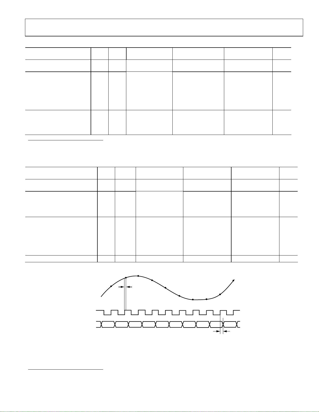
Output Delay1 (tOD) Full VI 2.5 4.8 6.5 2.5 4.8 6.5 2.5 4.8 6.5 ns
Pipeline Delay (Latency) Full V 5 5 5 Cycles
Aperture Delay 25°C V 2.4 2.4 2.4 ns
Aperture Uncertainty (Jitter) 25°C V 0.5 0.5 0.5 ps rms
Wake-Up Time2 25°C V 7 7 7 ms
OUT-OF-RANGE RECOVERY TIME 25°C V 1 1 1 Cycles
N+1
ANALOG
INPUT
N–1
N
t
N+2
A
N+3
AD9215BRU-80/
AD9215BCP-80
AD9215BRU-80/
AD9215BCP-80
N+4
N+5
N+6
AD9215BRU-105/
AD9215BCP-105
AD9215BRU-105/
N+8
N+7
AD9215BCP-105
Unit
CLK
DATA
OUT
N–7 N–6 N–5 N–4 N–3 N–2 N–1 N N+1 N+2
t
PD
Figure 2. Timing Diagram
02874-A-002
1
Output delay is measured from CLK 50% transition to DATA 50% transition, with 5 pF load on each output.
2
Wake-up time is dependent on the value of decoupling capacitors; typical values shown with 0.1 µF and 10 µF capacitors on REFT and REFB.
Rev. A | Page 5 of 36
AD9215
ABSOLUTE MAXIMUM RATINGS
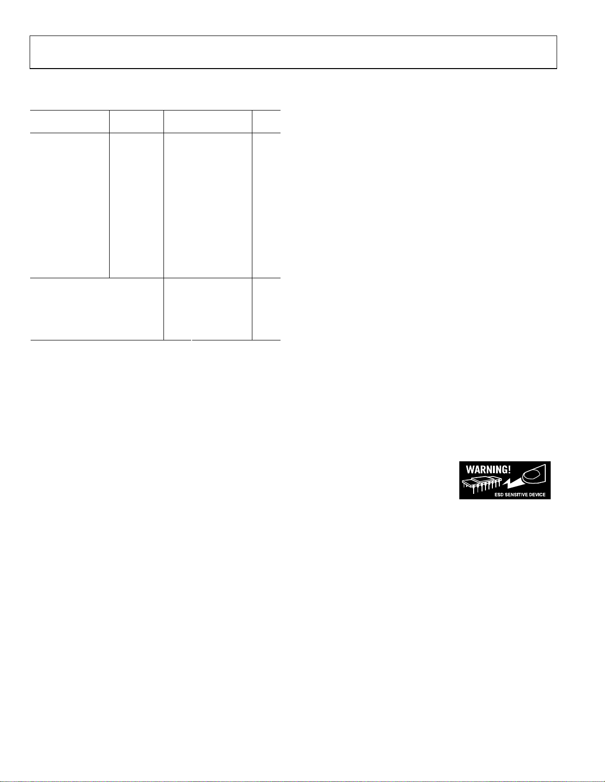
Table 5.
Mnemonic
ELECTRICAL
AVDD AGND −0.3 +3.9 V
DRVDD DRGND −0.3 +3.9 V
AGND DRGND −0.3 +0.3 V
AVDD DRVDD −3.9 +3.9 V
Digital Outputs DRGND −0.3 DRVDD + 0.3 V
CLK, MODE AGND −0.3 AVDD + 0.3 V
VIN+, VIN− AGND −0.3 AVDD + 0.3 V
VREF AGND −0.3 AVDD + 0.3 V
SENSE AGND −0.3 AVDD + 0.3 V
REFB, REFT AGND −0.3 AVDD + 0.3 V
PDWN AGND −0.3 AVDD + 0.3 V
ENVIRONMENTAL
Operating Temperature
Junction Temperature
Lead Temperature (10 sec)
Storage Temperature
NOTES
1
Absolute maximum ratings are limiting values to be applied individually, and
beyond which the serviceability of the circuit may be impaired. Functional
operability is not necessarily implied. Exposure to absolute maximum rating
conditions for an extended period of time may affect device reliability.
2
Typical thermal impedances 28-lead TSSOP: θJA = 67.7°C/W, 32-lead LFCSP:
= 32.7°C/W; heat sink soldered down to ground plane.
θ
JA
With
Respect to Min Max
2
−40 +85 °C
150 °C
300 °C
−65 +150 °C
1
Unit
EXPLANATION OF TEST LEVELS
Tes t Le v el
I 100% production tested.
II 100% production tested at 25°C and sample tested at
specified temperatures.
III Sample tested only.
IV Parameter is guaranteed by design and characterization
testing.
V Parameter is a typical value only.
VI 100% production tested at 25°C; guaranteed by design and
characterization testing for industrial temperature range;
100% production tested at temperature extremes for military devices.
ESD CAUTION
ESD (electrostatic discharge) sensitive device. Electrostatic charges as high as 4000 V readily accumulate on the
human body and test equipment and can discharge without detection. Although this product features
proprietary ESD protection circuitry, permanent damage may occur on devices subjected to high energy
electrostatic discharges. Therefore, proper ESD precautions are recommended to avoid performance
degradation or loss of functionality.
Rev. A | Page 6 of 36
AD9215
PIN CONFIGURATIONS AND FUNCTION DESCRIPTIONS
OR
1
MODE
2
SENSE
3
4
VREF
5
REFB
6
REFT
AVDD
AGND
VIN+
VIN–
AGND
AVDD
PDWN
AD9215
TOP VIEW
7
(Not to Scale)
8
9
10
11
12
13
CLK
14
DNC = DO NOT CONNECT
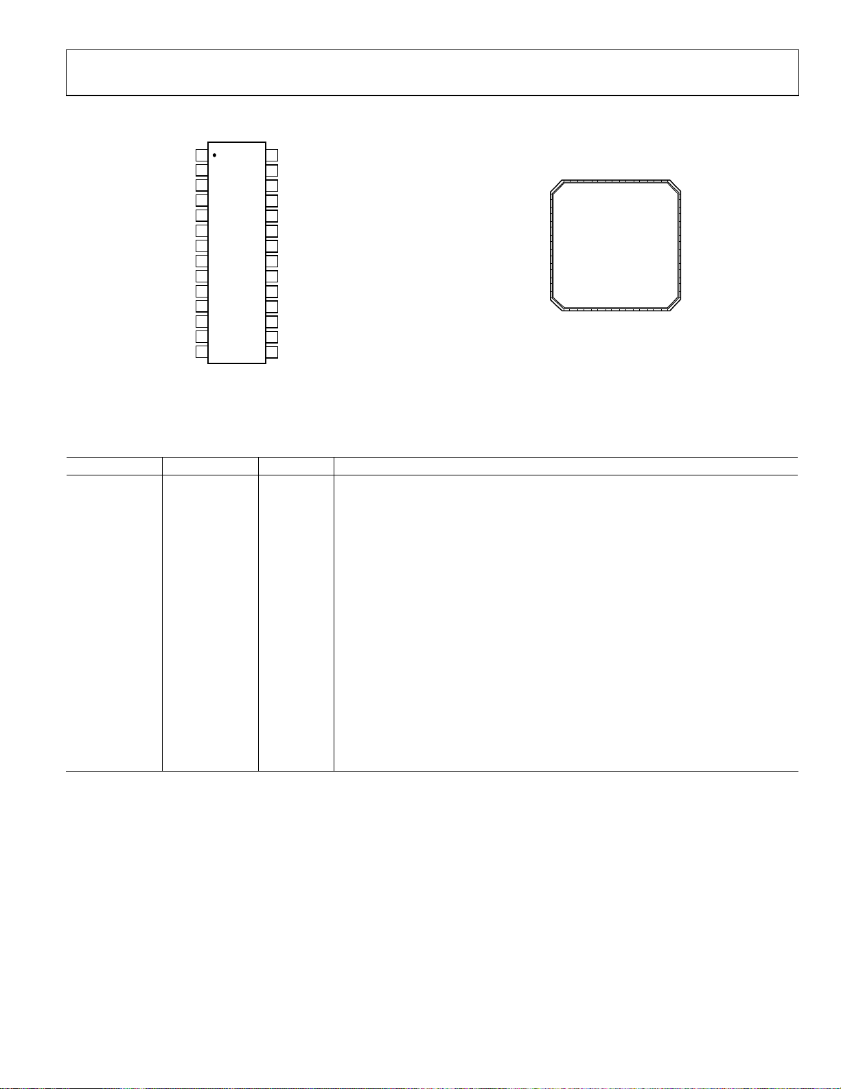
Figure 3. TSSOP (RU-28)
28
27
26
25
24
23
22
21
20
19
18
17
16
15
D9 (MSB)
D8
D7
D6
DRVDD
DRGND
D5
D4
D3
D2
D1
D0 (LSB)
DNC
DNC
32 AVDD
31 AGND
30 VIN–
29 VIN+
28 AGND
27 AVDD
26 REFT
25 REFB
DNC 1
CLK 2
DNC 3
PDWN 4
DNC 5
DNC 6
DNC 7
DNC 8
02874-A-003
DNC = DO NOT CONNECT
(Not to Scale)
D1 10
(LSB) D0 9
AD9215
TOP VIEW
D2 11
D3 12
D4 13
D5 14
DRVDD 16
DRGND 15
Figure 4. LFCSP (CP-32)
Table 6. Pin Function Descriptions
TSSOP Pin No. LFCSP Pin No. Mnemonic Description
1 21 OR Out-of-Range Indicator.
2 22 MODE Data Format and Clock Duty Cycle Stabilizer (DCS) Mode Selection.
3 23 SENSE Reference Mode Selection.
4 24 VREF Voltage Reference Input/Output.
5 25 REFB Differential Reference (Negative).
6 26 REFT Differential Reference (Positive).
7, 12 27, 32 AVDD Analog Power Supply.
8, 11 28, 31 AGND Analog Ground.
9 29 VIN+ Analog Input Pin (+).
10 30 VIN− Analog Input Pin (−).
13 2 CLK Clock Input Pin.
14 4 PDWN Power-Down Function Selection (Active High).
15 to 16 1, 3, 5 to 8 DNC Do not connect, recommend floating this pin.
17 to 22,
25 to 28
9 to 14,
17 to 20
D0 (LSB) to
D9 (MSB)
Data Output Bits.
23 15 DRGND Digital Output Ground.
24 16 DRVDD
Digital Output Driver Supply. Must be decoupled to DRGND with a
minimum 0.1 µF capacitor. Recommended decoupling is 0.1 µF in parallel with 10 µF.
24 VREF
23 SENSE
22 MODE
21 OR
20 D9 (MSB)
19 D8
18 D7
17 D6
02874-A-004
Rev. A | Page 7 of 36
AD9215
EQUIVALENT CIRCUITS
AVDD
MODE
02874-A-005
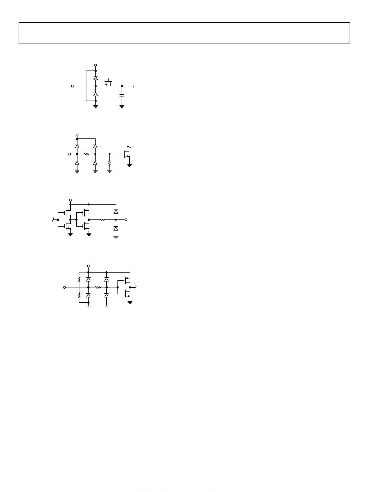
Figure 5. Equivalent Analog Input Circuit
AVDD
MODE
20kΩ
02874-A-006
Figure 6. Equivalent MODE Input Circuit
DRVDD
D9–D0,
OR
02874-A-007
Figure 7. Equivalent Digital Output Circuit
AVDD
2.6kΩ
CLK
2.6kΩ
02874-A-008
Figure 8. Equivalent Digital Input Circuit
DEFINITIONS OF SPECIFICATIONS
Aperture Delay
Aperture delay is a measure of the sample-and-hold amplifier
(SHA) performance and is measured from the rising edge of the
clock input to when the input signal is held for conversion.
Aperture Jitter
Aperture jitter is the variation in aperture delay for successive
samples and can be manifested as frequency-dependent noise
on the input to the ADC.
Clock Pulse Width and Duty Cycle
Pulse width high is the minimum amount of time that the clock
pulse should be left in the Logic 1 state to achieve rated performance. Pulse width low is the minimum time the clock pulse
should be left in the low state. At a given clock rate, these speci-
fications define an acceptable clock duty cycle.
Differential Nonlinearity (DNL, No Missing Codes)
An ideal ADC exhibits code transitions that are exactly 1 LSB
apart. DNL is the deviation from this ideal value. Guaranteed
no missing codes to 10-bit resolution indicate that all 1024
codes, respectively, must be present over all operating ranges.
Effective Number of Bits (ENOB)
For a sine wave, SINAD can be expressed in terms of the number of bits. Using the following formula, it is possible to obtain a
measure of performance expressed as N, the effective number of
bits
N = (SINAD – 1.76)/6.02
Thus, the effective number of bits for a device for sine wave
inputs at a given input frequency can be calculated directly
from its measured SINAD.
Gain Error
The first code transition should occur at an analog value 1/2
LSB above negative full scale. The last transition should occur at
an analog value 1 1/2 LSB below the positive full scale. Gain
error is the deviation of the actual difference between the first
and last code transitions and the ideal difference between the
first and last code transitions.
Integral Nonlinearity (INL)
INL refers to the deviation of each individual code from a line
drawn from “negative full scale” through “positive full scale.”
The point used as negative full scale occurs 1/2 LSB before the
first code transition. Positive full scale is defined as a level 1 1/2
LSB beyond the last code transition. The deviation is measured
from the middle of each particular code to the true straight line.
Maximum Conversion Rate
The clock rate at which parametric testing is performed.
Minimum Conversion Rate
The clock rate at which the SNR of the lowest analog signal
frequency drops by no more than 3 dB below the guaranteed
limit.
Offset Error
The major carry transition should occur for an analog value 1/2
LSB below VIN+ = VIN−. Zero error is defined as the deviation
of the actual transition from that point.
Out-of-Range Recovery Time
Out-of-range recovery time is the time it takes for the ADC to
reacquire the analog input after a transient from 10% above
positive full scale to 10% above negative full scale, or from 10%
below negative full scale to 10% below positive full scale.
Output Propagation Delay
The delay between the clock logic threshold and the time when
Rev. A | Page 8 of 36

AD9215
all bits are within valid logic levels.
Power Supply Rejection
The specification shows the maximum change in full scale from
the value with the supply at the minimum limit to the value
with the supply at its maximum limit.
Signal-to-Noise and Distortion (SINAD) Ratio
SINAD is the ratio of the rms value of the measured input signal to the rms sum of all other spectral components below the
Nyquist frequency, including harmonics but excluding dc. The
value for SINAD is expressed in decibels.
Signal-to-Noise Ratio (SNR)
SNR is the ratio of the rms value of the measured input signal to
the rms sum of all other spectral components below the Nyquist
frequency, excluding the first six harmonics and dc. The value
for SNR is expressed in decibels.
Spurious-Free Dynamic Range (SFDR)
SFDR is the difference in dB between the rms amplitude of the
input signal and the peak spurious signal.
Temperature Drift
The temperature drift for zero error and gain error specifies the
maximum change from the initial (25°C) value to the value at
or T
T
MIN
MAX
.
Total Harmonic Distortion (THD)
THD is the ratio of the rms sum of the first six harmonic components to the rms value of the measured input signal and is
expressed as a percentage or in decibels.
Two-Tone SFDR
The ratio of the rms value of either input tone to the rms value
of the peak spurious component. The peak spurious component
may or may not be an IMD product. It may be reported in dBc
(i.e., degrades as signal levels are lowered) or in dBFS (always
related back to converter full scale).
Rev. A | Page 9 of 36
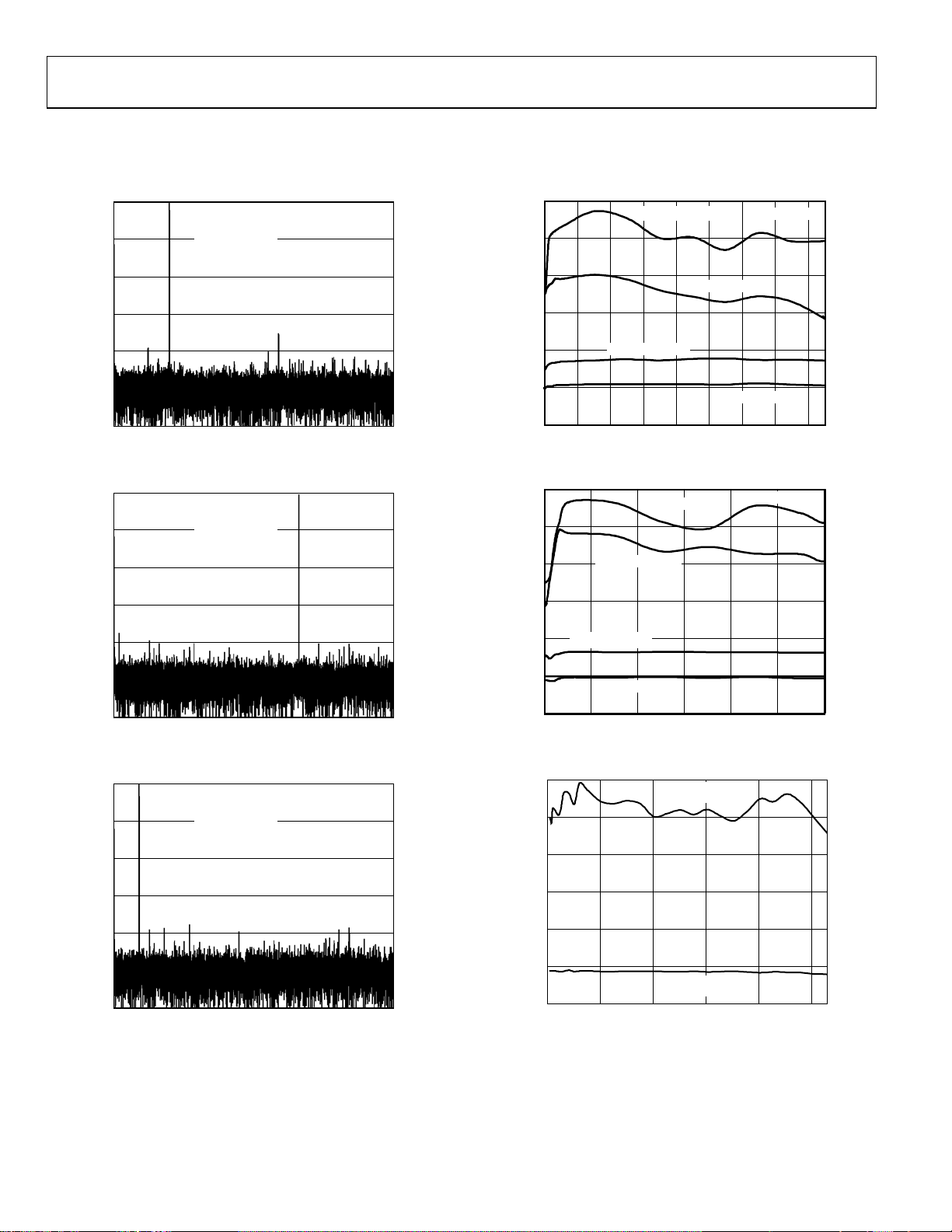
AD9215
TYPICAL PERFORMANCE CHARACTERISTICS
AVDD = 3.0 V, DRVDD = 2.5 V with DCS enabled, TA = 25°C, 2 V differential input, AIN = −0.5 dBFS, VREF = 1.0 V, unless
otherwise noted.
80
75
70
2V p-p SFDR (dBc)
1V p-p SFDR (dBc)
AIN = –0.5dBFS
–20
–40
0
AIN = –0.5dBFS
SNR = 58.0
ENOB = 9.4 BITS
SFDR = 75.5dB
–60
–80
AMPLITUDE (dBFS)
–100
–120
0 52.5045.9439.3832.8126.2519.6913.136.56
FREQUENCY (MHz)
Figure 9. Single-Tone 32k FFT with f
0
AIN = –0.5dBFS
SNR = 57.8
ENOB = 9.4 BITS
SFDR = 75.0dB
FREQUENCY (MHz)
AMPLITUDE (dBFS)
–100
–120
–20
–40
–60
–80
0 52.5045.9439.3832.8126.2519.6913.136.56
Figure 10. Single-Tone 32k FFT with f
0
AIN = –0.5dBFS
–20
–40
SNR = 57.7
ENOB = 9.3 BITS
SFDR = 75dB
= 10.3 MHZ, f
IN
= 70.3 MHz, f
IN
SAMPLE
SAMPLE
= 105 MSPS
= 105 MSPS
65
dB
60
55
02874-A-062
50
5 1525354555657585
Figure 12. AD9215-80 SNR/SFDR vs. f
80
75
70
65
dB
60
55
02874-A-063
50
5 152535455565
Figure 13. AD9215-65 SNR/SFDR vs. f
85
80
75
2V p-p SNR (dB)
1V p-p SFDR (dBc)
2V p-p SNR (dB)
1V p-p SNR (dB)
ENCODE (MSPS)
2V p-p SFDR (dBc)
ENCODE (MSPS)
2V p-p SFDR
1V p-p SNR (dB)
, fIN = 10.3 MHz
SAMPLE
AIN = –0.5dBFS
, fIN = 10.3 MHz
SAMPLE
02874-A-012
02874-A-013
–60
–80
AMPLITUDE (dBFS)
–100
–120
0 52.5045.9439.3832.8126.2519.6913.136.56
FREQUENCY (MHz)
Figure 11. Single-Tone 32k FFT with f
= 100.3 MHz, f
IN
= 105 MSPS
SAMPLE
02874-A-065
Rev. A | Page 10 of 36
70
dB
65
60
55
0 10080604020
f
SAMPLE
Figure 14. AD9215-105 SNR/SFDR vs. f
2V p-p SNR
(MSPS)
, fIN = 10.3 MHz
SAMPLE
02874-A-066
AD9215
80
80
70
60
80dB REFERENCE LINE
50
40
dB
30
20
10
0
–50 –40–45 –35 –25–30 –10–15–20 –5 0
2V p-p SFDR (dBc)
ANALOG INPUT LEVEL
1V p-p SFDR (dBc)
2V p-p SNR (dB)
1V p-p SNR (dB)
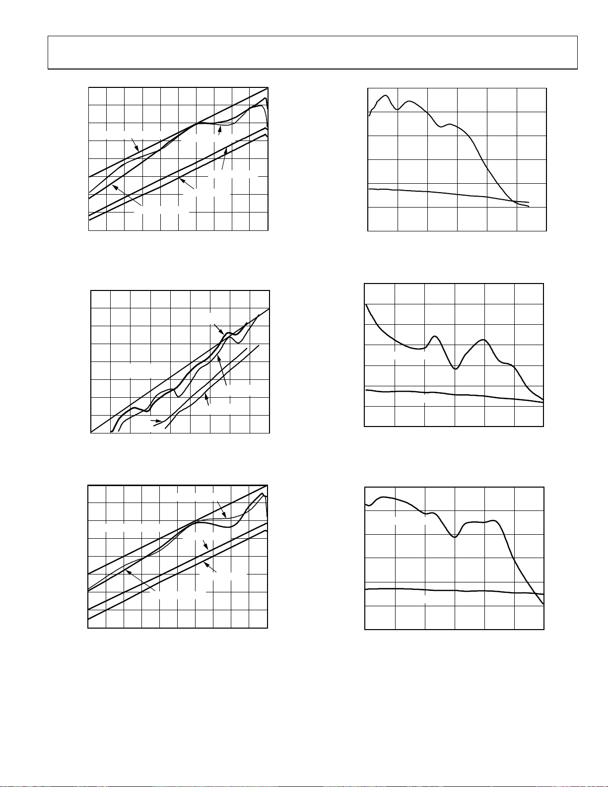
Figure 15. AD9215-80 SNR/SFDR vs.
Analog Input Drive Level, f
80
70
60
50
40
dB
30
20
10
0
–90 –80 –70 –60 –50 –40 –30 –20 –10 0
–70dBFS
REFERENCE LINE
2V p-p
SNR
ANALOG INPUT LEVEL (–dBFS)
= 80 MSPS, fIN = 39.1 MHz
SAMPLE
2 SFDR dBc
1V p-p SFDR (dBc)
1V p-p SNR
Figure 16. AD9215-105 SNR/SFDR vs.
Analog Input Drive Level, f
80
70
60
80dB REFERENCE LINE
50
= 105 MSPS, fIN = 50.3 MHz
SAMPLE
1V p-p SFDR (dBc)
2V p-p SNR (dB)
75
SFDR
70
65
dB
60
55
02874-A-014
50
0 50 100 150 200 250 300
SNR
FREQUENCY (MHz)
02874-A-072
Figure 18. AD9215-105 SNR/SFDR vs.
, AIN = −0.5 dBFS, f
f
IN
85
80
75
70
dB
65
60
55
02874-A-067
50
2V p-p SFDR (dBc)
2V p-p SNR (dB)
0 10050 150 250200 300
f
IN
SAMPLE
(MHz)
= 105 MSPS
02874-A-016
Figure 19. AD9215-80 SNR/SFDR vs.
fIN, AIN = −0.5 dBFS, f
80
75
2V p-p SFDR (dBc)
70
SAMPLE
= 80 MSPS
40
dB
30
20
10
0
–50 –40–45 –35 –25–30 –10–15–20 –5 0
2V p-p SFDR (dBc)
ANALOG INPUT LEVEL
1V p-p SNR (dB)
Figure 17. AD9215-65 SNR/SFDR vs.
Analog Input Drive Level, f
= 65 MSPS, fIN = 30.3 MHz
SAMPLE
02874-A-015
Rev. A | Page 11 of 36
65
dB
60
55
50
0 10050 150 250200 300
2V p-p SNR (dB)
ANALOG INPUT (MHz)
Figure 20. AD9215-65 SNR/SFDR vs.
, AIN = −0.5 dBFS, f
f
IN
SAMPLE
= 65 MSPS
02874-A-017
 Loading...