10-Bit, 65/80/105 MSPS
a
FEATURES
SNR = 57 dB @ 39 MHz Analog Input (–0.5 dBFS)
Low Power
190 mW at 65 MSPS
285 mW at 105 MSPS
30 mW Power-Down Mode
300 MHz Analog Bandwidth
On-Chip Reference and Track/Hold
1 V p-p or 2 V p-p Analog Input Range Option
Single 3.3 V Supply Operation (2.7 V–3.6 V)
Two’s Complement or Offset Binary Data Format Option
APPLICATIONS
Battery-Powered Instruments
Hand-Held Scopemeters
Low-Cost Digital Oscilloscopes
Ultrasound Equipment
Cable Reverse Path
Broadband Wireless
Residential Power Line Networks
A
A
ENCODE
IN
IN
3 V A/D Converter
AD9214
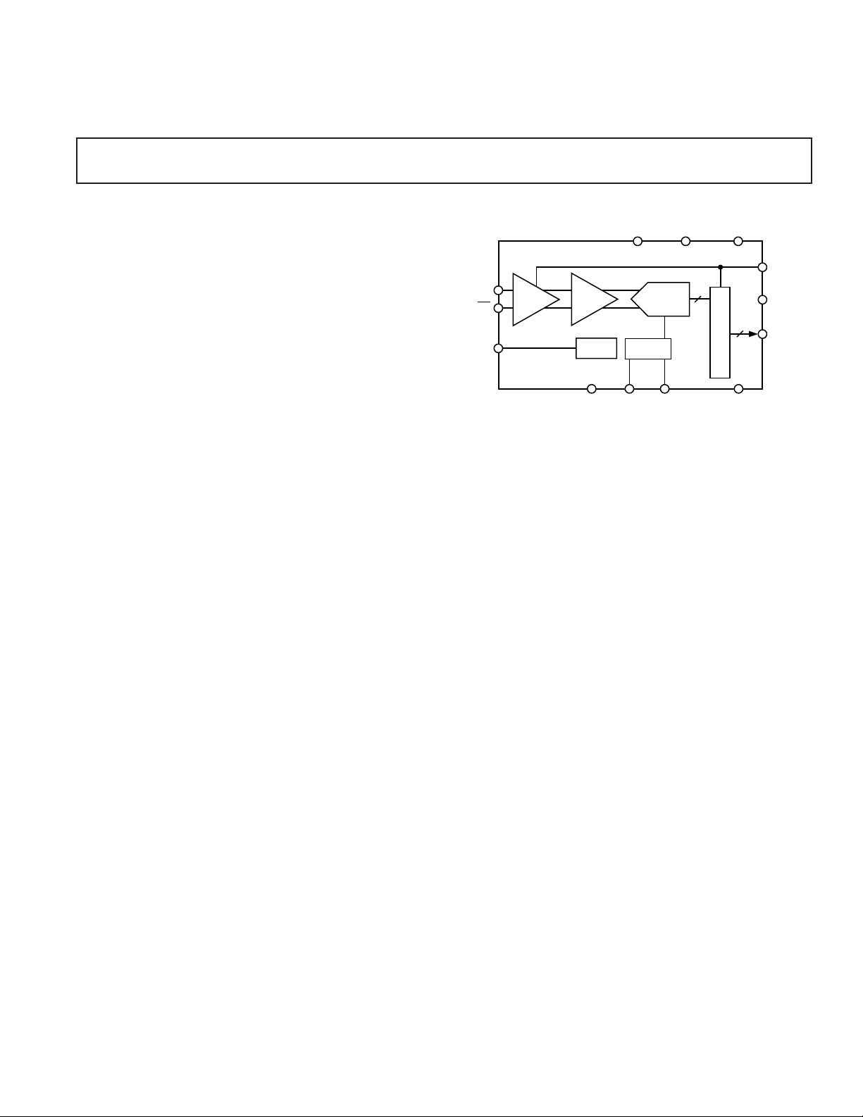
FUNCTIONAL BLOCK DIAGRAM
PWRDWN
AV
DD
AD9214
T/HBUFFER
AGND
REF
PIPELINE
REFTIMING
REFSENSE
ADC
CORE
10
DrV
DD
DFS/GAIN
OR
10
D
9–D0
OUTPUT REGISTER
DGND
PRODUCT DESCRIPTION
The AD9214 is a 10-bit monolithic sampling analog-to-digital
converter (ADC) with an on-chip track-and-hold circuit, and
is optimized for low cost, low power, small size, and ease of use.
The product operates up to 105 MSPS conversion rate with
outstanding dynamic performance over its full operating range.
The ADC requires only a single 3.3 V (2.7 V to 3.6 V) power
supply and an encode clock for full performance operation. No
external reference or driver components are required for many
applications. The digital outputs are TTL/CMOS compatible
and a separate output power supply pin supports interfacing
with 3.3 V or 2.5 V logic.
The clock input is TTL/CMOS compatible. In the power-down
state, the power is reduced to 30 mW. A gain option allows
support for either 1 V p-p or 2 V p-p analog signal input swing.
Fabricated on an advanced CMOS process, the AD9214 is
available in a 28-lead surface-mount plastic package (28-SSOP)
specified over the industrial temperature range (–40°C to +85°C).
PRODUCT HIGHLIGHTS
High Performance—Outstanding ac performance from 65 MSPS
to 105 MSPS. SNR greater than 55 dB typical and as high
as 58 dB.
Low Power—The AD9214 at 285 mW consumes a fraction of
the power available in existing high-speed monolithic solutions.
In sleep mode, power is reduced to 30 mW.
Single Supply—The AD9214 uses a single 3 V supply, simplifying system power supply design. It also features a separate digital
output driver supply line to accommodate 2.5 V logic families.
Small Package—The AD9214 is packaged in a small 28-lead
surface-mount plastic package (28-SSOP).
REV. D
Information furnished by Analog Devices is believed to be accurate and
reliable. However, no responsibility is assumed by Analog Devices for its
use, nor for any infringements of patents or other rights of third parties that
may result from its use. No license is granted by implication or otherwise
under any patent or patent rights of Analog Devices.
One Technology Way, P.O. Box 9106, Norwood, MA 02062-9106, U.S.A.
Tel: 781/329-4700 www.analog.com
Fax: 781/326-8703 © Analog Devices, Inc., 2002

AD9214–SPECIFICATIONS
(AVDD = 3 V, DrVDD = 3 V; T
DC SPECIFICATIONS
frequency used, unless otherwise noted.)
= –40ⴗC, T
MIN
= +85ⴗC; external 1.25 V voltage reference and rated encode
MAX
Parameter Temp Level Min Typ Max Min Typ Max Min Typ Max Unit
Test AD9214-65 AD9214-80 AD9214-105
RESOLUTION 10 10 10 Bits
ACCURACY
No Missing Codes 25°C VI Guaranteed Guaranteed Guaranteed
Full VI Guaranteed Guaranteed
Offset Error Full VI –18 0 +18 –18 0 +18 –18 0 +18 LSB
Gain Error
Differential Nonlinearity
Integral Nonlinearity
1
2
(DNL) Full V –1.0 +1.2 –1.0 +1.4 +1.7 LSB
2
25°C I –2 +8 –2 +8 –2 +8 % FS
25°C I –1.0 ± 0.5 +1.0 –1.0 ±0.5 +1.2 –1.0 ±0.8 +1.5 LSB
25°C I –1.35 ± 0.75 +1.35 –1.5 ±0.75 +1.5 –2.2 ± 1.5 +2.2 LSB
(INL) Full V –1.9 +1.9 –1.8 +1.8 –2.5 +2.5 LSB
TEMPERATURE DRIFT
Offset Error Full V 16 16 16 ppm/°C
Gain Error
1
Full V 150 150 150 ppm/°C
Reference Voltage Full V 80 80 80 ppm/°C
REFERENCE (REF)
Internal Reference Voltage 25°C VI 1.18 1.23 1.28 1.18 1.23 1.28 1.18 1.23 1.28 V
Output Current
Input Current
3
4
Full V 200 200 200 µA
Full V 123 123 123 µA
Input Resistance Full V 10 10 10 kΩ
ANALOG INPUTS (AIN, AIN)
Differential Input Range Full V 1 or 2 1 or 2 1 or 2 V p-p
Common-Mode Voltage Full V AVDD/3 AVDD/3 AVDD/3 V
Differential Input Resistance5Full V 20 20 20 kΩ
Differential Input Capacitance Full V 5 5 5 pF
POWER SUPPLY
Supply Voltages
AV
DD
DrV
DD
Supply Current
I
(AVDD = 3.0 V)
AVDD
Power-Down Current
I
(AVDD = 3.0 V) Full VI 10 15 10 15 10 15 mA
AVDD
Power Consumption
6
7
8
Full IV 2.7 3.6 2.7 3.6 2.7 3.6 V
Full IV 2.7 3.6 2.7 3.6 2.7 3.6 V
Full VI 64 75 90 105 95 110 mA
Full VI 190 220 250 300 285 325 mW
PSRR 25°CI ±0.5 ±1 ±1 LSB/V
Full V ±2 ±2 ± 2 mV/V
NOTES
1
Gain error and gain temperature coefficient are based on the ADC only (with a fixed 1.25 V external reference).
2
Measured with 1 V AIN range for AD9214-80 and AD9214-105. Measured with 2 V AIN range for AD9214-65.
3
REFSENSE externally connected to AGND, REF is configured as an output for the internal reference voltage.
4
REFSENSE externally connected to AVDD, REF is configured as an input for an external reference voltage.
5
10 kΩ to AVDD/3 on each input.
6
I
is measured with an analog input of 10.3 MHz, 0.5 dBFS, sine wave, rated encode rate, and PWRDN = 0. See Typical Performance Characteristics and
AVDD
Applications section for I
7
Power-down supply currents measured with PWRDN = 1; rated encode rate, AIN = full-scale dc input.
8
Power consumption measured with AIN = full-scale dc input.
Specifications subject to change without notice.
DrVDD
.
–2–
REV. D

AD9214
DIGITAL SPECIFICATIONS
Parameter Temp Level Min Typ Max Min Typ Max Min Typ Max Unit
DIGITAL INPUTS
Logic “1” Voltage Full IV 2.0 2.0 2.0 V
Logic “0” Voltage Full IV 0.8 0.8 0.8 V
Input Capacitance Full V 2.0 2.0 2.0 pF
DIGITAL OUTPUTS
Logic Compatibility CMOS/TTL CMOS/TTL CMOS/TTL V
Logic “1” Voltage Full VI DrV
Logic “0” Voltage Full VI 50 50 50 mV
NOTES
1
Digital Inputs include ENCODE and PWRDN.
2
Digital Outputs include D0–D9 and OR.
Specifications subject to change without notice.
AC SPECIFICATIONS
Parameter Temp Level Min Typ Max Min Typ Max Min Typ Max Unit
SNR
Analog Input 10 MHz 25°C I 55.5 58.3 56.0 58.1 51.0 53.0 dB
@ –0.5 dBFS 39 MHz 25°C I 57.1 55.0 57.1 50.5 53.0 dB
SINAD
Analog Input 10 MHz 25°C I 55.0 57.8 55.5 57.6 50.0 52.0 dB
@ –0.5 dBFS 39 MHz 25°C I 56.7 54.5 56.7 50.0 52.0 dB
EFFECTIVE NUMBER OF BITS
Analog Input 10 MHz 25°C I 8.9 9.3 9.0 9.3 8.4 Bit
@ –0.5 dBFS 39 MHz 25°C I 9.2 8.8 9.2 8.4 Bit
SECOND HARMONIC DISTORTION
Analog Input 10 MHz 25°C I –66 –79 –64 –74 –62 –68 dBc
@ –0.5 dBFS 39 MHz 25°C I –75 –63 –76 –62 –71 dBc
THIRD HARMONIC DISTORTION
Analog Input 10 MHz 25°C I –63.5 –71 –63 –72 –59 –64 dBc
@ –0.5 dBFS 39 MHz 25°C I –70 –63 –74 –59 –67 dBc
SFDR
Analog Input 10 MHz 25°C I 63.5 71 63 71 57 62 dBc
@ –0.5 dBFS 39 MHz 25°C I 70 63 71 57 62 dBc
TWO-TONE INTERMOD DISTORTION
Analog Input @ –0.5 dBFS 25°C V 76 74 72 dBFS
ANALOG INPUT BANDWIDTH 25°C V 300 300 300 MHz
NOTES
1
AC specifications based on a 1.0 V p-p full-scale input range for the AD9214-80 and AD9214-105, and a 2.0 V p-p full-scale input range for the AD9214-65. An
external reference is used.
2
F1 = 29.3 MHz, F2 = 30.3 MHz.
Specifications subject to change without notice.
1
2
1
51 MHz 25°C V 55.0 53.0 dB
70 MHz 25°C V 54.0 52.6 dB
51 MHz 25°C V 54.5 52.0 dB
70 MHz 25°C V 52.0 dB
51 MHz 25°C V 8.8 8.4 Bit
70 MHz 25°C V 8.5 8.4 Bit
51 MHz 25°C V –72 –64 dBc
70 MHz 25°C V –65 –62 dBc
51 MHz 25°C V –78 –71 dBc
70 MHz 25°C V –65 dBc
51 MHz 25°C V 67 62 dBc
70 MHz 25°C V 64 62 dBc
(AV
= 3 V, DrVDD = 3 V; T
DD
Test AD9214-65 AD9214-80 AD9214-105
– 50 mV DrVDD – 50 mV DrVDD – 50 mV V
DD
= –40ⴗC, T
MIN
= +85ⴗC)
MAX
(AVDD = 3 V, DrVDD = 3 V; ENCODE = Maximum Conversion Rate; T
1.25 V voltage reference used, unless otherwise noted.)
Test AD9214-65 AD9214-80 AD9214-105
2
= –40ⴗC, T
MIN
= +85ⴗC; external
MAX
REV. D
–3–

AD9214–SPECIFICATIONS
(AVDD = 3 V, DrVDD = 3 V; ENCODE = Maximum Conversion Rate; T
SWITCHING SPECIFICATIONS
external 1.25 V voltage reference used, unless otherwise noted.)
= –40ⴗC, T
MIN
= +85ⴗC;
MAX
Parameter Temp Level Min Typ Max Min Typ Max Min Typ Max Unit
Test AD9214-65 AD9214-80 AD9214-105
ENCODE INPUT PARAMETERS*
Maximum Conversion Rate Full VI 65 80 105 MSPS
Minimum Conversion Rate Full IV 20 20 20 MSPS
Encode Pulsewidth High (t
) Full IV 6.0 5.0 3.8 ns
EH
Encode Pulsewidth Low (tEL) Full IV 6.0 5.0 3.8 ns
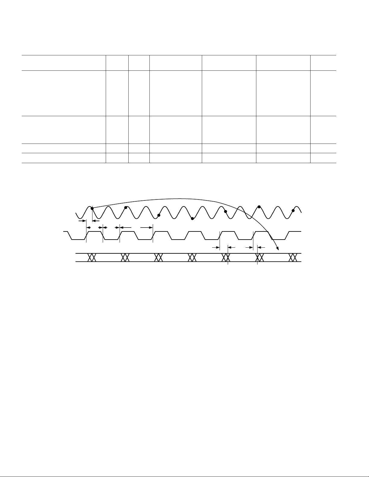
Aperture Delay (tA)25°C V 2.0 2.0 2.0 ns
Aperture Uncertainty (Jitter) 25°C V 3 3 3 ps rms
DATA OUTPUT PARAMETERS
Pipeline Delays Full IV 5 5 5 Clock Cycle
Output Valid Time (tV)* Full V 3.0 4.5 3.0 4.5 3.0 4.5 ns
Output Propagation Delay* (tPD) Full V 4.5 6.0 4.5 6.0 4.5 6.0 ns
TRANSIENT RESPONSE TIME 25°CV555ns
OUT-OF-RANGE RECOVERY TIME 25°CV555ns
*
tV and tPD are measured from the 1.5 V level of the ENCODE input to the 50% levels of the digital output swing. The digital output load during test is not to exceed
an ac load of 5 pF or a dc current of ± 40 µA.
Specifications subject to change without notice.
SAMPLE N+5
A
ENCODE
SAMPLE N
IN
t
A
t
t
EH
EL
SAMPLE N+1
1/F
S
SAMPLE N+2
SAMPLE N+3
SAMPLE N+4
D9 – D0
t
PD
DATA N–5 DATA N–4 DATA N–3 DATA N–2 DATA N–1 DATA N
t
V
Figure 1. Timing Diagram
–4–
REV. D

AD9214
WARNING!
ESD SENSITIVE DEVICE
ABSOLUTE MAXIMUM RATINGS
Electrical
Voltage . . . . . . . . . . . . . . . . . . . . . . . . . . . . . 4 V max
AV
DD
Voltage . . . . . . . . . . . . . . . . . . . . . . . . . . . . 4 V max
DrV
DD
Analog Input Voltage . . . . . . . . . . . –0.5 V to AV
Analog Input Current . . . . . . . . . . . . . . . . . . . . . . . 0.4 mA
Digital Input Voltage . . . . . . . . . . . –0.5 V to AV
Digital Output Current . . . . . . . . . . . . . . . . . . 20 mA max
REF Input Voltage . . . . . . . . . . . . . –0.5 V to AV
Environmental
2
Operating Temperature Range (Ambient)
. . . . . . . . . . . . . . . . . . . . . . . . . . . . . . . –40°C to +125°C
1
EXPLANATION OF TEST LEVELS
I 100% production tested.
II 100% production tested at 25°C and guaranteed by design
+ 0.5 V
DD
+ 0.5 V
DD
and characterization at specified temperatures.
III Sample Tested Only
IV Parameter is guaranteed by design and characterization
testing.
+ 0.5 V
DD
V Parameter is a typical value only.
VI 100% production tested at 25°C and guaranteed by design
and characterization for industrial temperature range.
Maximum Junction Temperature . . . . . . . . . . . . . . . 150°C
Lead Temperature (Soldering, 10 sec) . . . . . . . . . . . 150°C
Storage Temperature Range (Ambient) . . . –65°C to +150°C
NOTES
1
Absolute maximum ratings are limiting values to be applied individually, and
beyond which the serviceability of the circuit may be impaired. Functional
operability is not necessarily implied. Exposure to absolute maximum rating conditions for an extended period of time may affect device reliability.
2
Typical thermal impedances (package = 28 SSOP); θJA = 49°C/W. These
measurements were taken on a 6-layer board in still air with a solid
ground plane.
ORDERING GUIDE
Model Temperature Range Package Description Package Option
AD9214BRS-65 –40°C to +85°C (Ambient) 28-Lead Shrink Small Outline Package RS-28
AD9214BRS-80 –40°C to +85°C (Ambient) 28-Lead Shrink Small Outline Package RS-28
AD9214BRS-105 –40°C to +85°C (Ambient) 28-Lead Shrink Small Outline Package RS-28
AD9214-65PCB 25°C Evaluation Board with AD9214-65
AD9214-105PCB 25°C Evaluation Board with AD9214-105
CAUTION
ESD (electrostatic discharge) sensitive device. Electrostatic charges as high as 4000 V readily
accumulate on the human body and test equipment and can discharge without detection. Although
the AD9214 features proprietary ESD protection circuitry, permanent damage may occur on
devices subjected to high-energy electrostatic discharges. Therefore, proper ESD precautions are
recommended to avoid performance degradation or loss of functionality.
REV. D
–5–

AD9214
PIN FUNCTION DESCRIPTIONS
Pin No. Mnemonic Function
1 OR CMOS Output; Out-of-Range Indicator. Logic HIGH indicates the analog input voltage was
outside the converter’s range for the current output data.
2 DFS/GAIN Data Format Select and Gain Mode Select. Connect externally to AV
data format and 1 V p-p analog input range. Connect externally to AGND for Offset Binary data
format and 1 V p-p analog input range. Connect externally to REF (Pin 4) for two’s complement
data format and 2 V p-p analog input range. Floating this pin will configure the device for Offset
Binary data format and a 2 V p-p analog input range.
3 REFSENSE Reference Mode Select Pin for the ADC. This pin is normally connected externally to AGND,
which enables the internal 1.25 V reference, and configures REF (Pin 4) as an analog reference
output pin. Connecting REFSENSE externally to AV
disables the internal reference, and config-
DD
ures REF (Pin 4) as an external reference input. In this case, the user must drive REF with a clean
and accurate 1.25 V (±5%) reference input.
4 REF Reference input or output as configured by REFSENSE (Pin 3). When configured as an output
(REFSENSE = AGND), the internal reference (nominally 1.25 V) is enabled and is available to
the user on this pin. When configured as an input (REFSENSE = AVDD), the user must drive
REF with a clean and accurate 1.25 V (±5%) reference. This pin should be bypassed to AGND
with an external 0.1 µF capacitor, whether it is configured as an input or output.
5, 8, 11 AGND Analog Ground
6, 7, 12 AV
9A
DD
IN
Analog Power Supply, Nominally 3 V
Positive terminal of the differential analog input for the ADC.
10 AIN Negative terminal of the differential analog input for the ADC. This pin can be left open if
operating in single-ended mode, but it is preferable to match the impedance seen at the positive
terminal (see Driving the Analog Inputs).
13 ENCODE Encode Clock for the ADC. The AD9214 samples the analog signal on the rising edge of ENCODE.
14 PWRDN CMOS-compatible power-down mode select, Logic LOW for normal operation; Logic HIGH
for power-down mode (digital outputs in high impedance state). PWRDN has an internal
10 kΩ pull-down resistor to ground.
15, 23 DGND Digital Output Ground
16, 24 DrV
DD
Digital Output Driver Power Supply. Nominally 2.5 V to 3.6 V.
17–22, 25–28 D0 (LSB)–D5, CMOS Digital Outputs of ADC
D6–D9 (MSB)
for two’s complement
DD
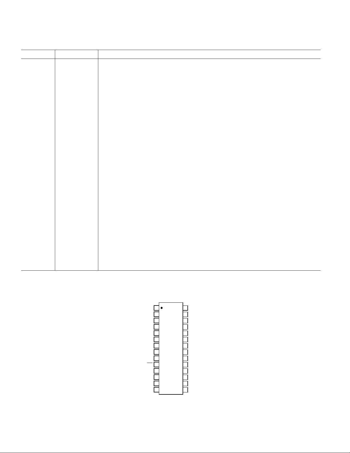
PIN CONFIGURATION
28-Lead Shrink Small Outline Package
1
OR
DFS/GAIN
REFSENSE
REF
AGND
AV
AV
AGND
A
A
AGND
AV
ENCODE
PWRDN
DD
DD
IN
10
IN
11
12
DD
13
14
2
3
4
5
6
AD9214
7
TOP VIEW
(Not to Scale)
8
9
28
27
26
25
24
23
22
21
20
19
18
17
16
15
D9 (MSB)
D8
D7
D6
DrV
DD
DGND
D5
D4
D3
D2
D1
D0 (LSB)
DrV
DD
DGND
–6–
REV. D
 Loading...