

现货库存、技术资料、百科信息、热点资讯,精彩尽在鼎好!
10-Bit, 170/200/250 MSPS
Preliminary Technical Data
FEATURES
SNR = 60 dBFs @ fIN up to 70 MHz @ 250 MSPS
ENOB of 9.7 @ f
SFDR = 80 dBc@ f
Excellent Linearity
DNL = ±0.3 LSB (Typical)
INL = ±0.5 LSB (Typical)
LVDS at 250 MSPS (ANSI-644 levels)
900 MHz Full Power Analog Bandwidth
On-Chip Reference and Track-and-Hold
Power Dissipation = 380 mW Typical @ 250 MSPS
1.25 V Input Voltage Range
1.8 V Analog Supply Operation
Output Data Format Option
Data Clock Output Provided
Clock Duty Cycle Stabilizer
APPLICATIONS
Wireless and Wired Broadband Communications
Cable Reverse Path
Communications Test Equipment
Radar and Satellite Subsystems
Power Amplifier Linearization
PRODUCT DESCRIPTION
The AD9211 is a 10-Bit monolithic sampling analog-to-digital
converter optimized for high performance, low power, and ease
of use. The product operates up to a 250 MSPS conversion rate
and is optimized for outstanding dynamic performance in
wideband carrier and broadband systems. All necessary
functions, including a track-and-hold (T/H) and voltage
reference, are included on the chip to provide a complete signal
conversion solution.
The ADC requires a 1.8 V analog voltage supply and a
differential clock for full performance operation. The digital
outputs are LVDS (ANSI-644) compatible and support either
twos complement, offset binary format or gray code. A data
clock output is available for proper output data timing.
up to 70 MHz @ 250 MSPS (–0.5 dBFS)
IN
up to 70 MHz @ 250 MSPS (–0.5 dBFS)
IN
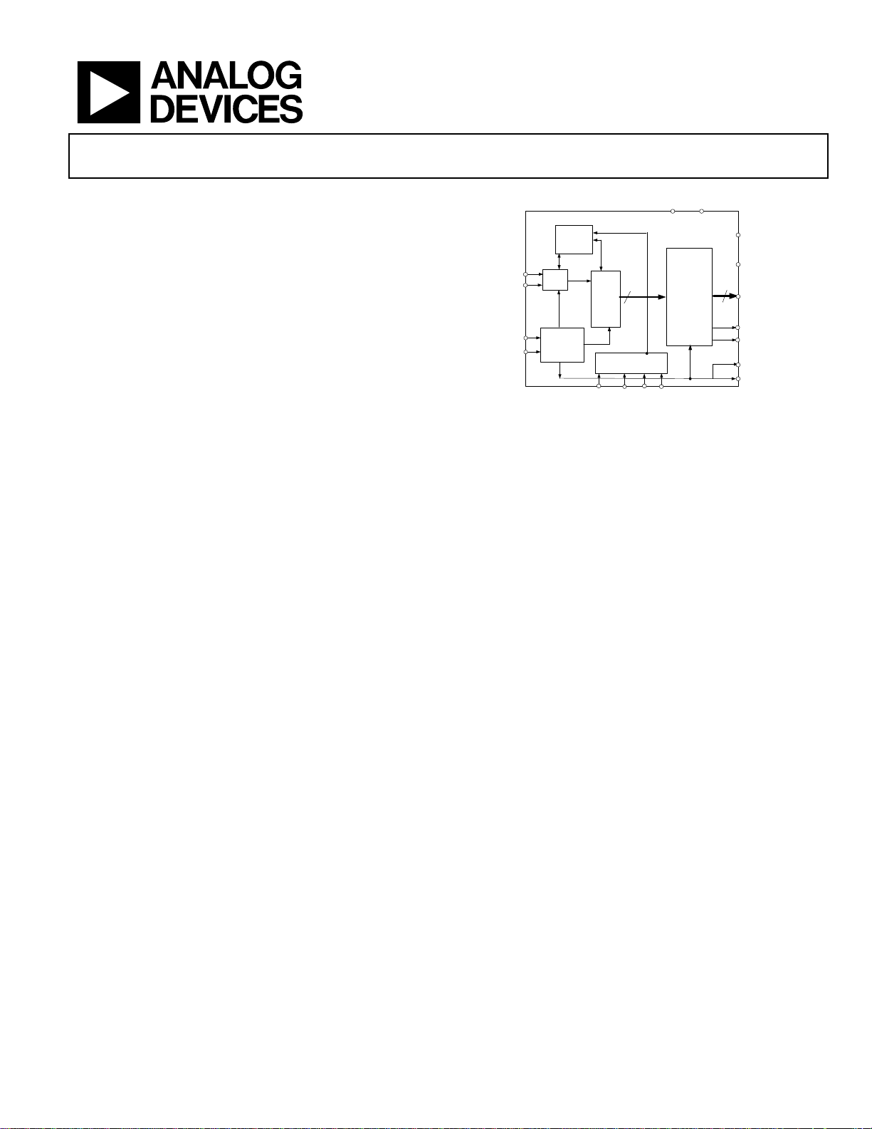
1.8 V A/D Converter
AD9211
AVDD (1.8V)
AGND
AD9211
Ref
VIN+
VIN-
CLK+
CLK-
T/H
Clock
Mgmt
RESET
ADC
10-bit
Core
10
Serial Port
SCLK CSB
SDIO
Output
Staging -
LVDS
Figure 1. Functional Block Diagram
Fabricated on an advanced CMOS process, the AD9211 is
available in a 56-lead chip scale package (56 LFCSP) specified
over the industrial temperature range (–40°C to +85°C).
PRODUCT HIGHLIGHTS
1. High Performance—Maintains 60 dB SNR @ 250 MSPS
with a 65 MHz input.
2. Low Power—Consumes only 380mW @ 250 MSPS.
3. Ease of Use—LVDS output data and output clock signal
allow interface to current FPGA technology. The on-chip
reference and sample/hold provide flexibility in system
design. Use of a single 1.8 V supply simplifies system
power supply design. Supported DDR mode reduces
number of output data traces
4. Serial Port Control - Standard serial port interface
supports various product functions such as data
formatting, enabling a clock duty cycle stabilizer, power
down, gain adjust and output test pattern generation.
Pin compatible family – 12-bit pin compatible family
5.
offered as AD9230.
DrVDD (1.8V)
DGND
(Pin 0)
10
D9-D0
(D4-D0 DDR mode)
OTR+
OTR-
DCO+
DCO-
Rev. PrA
Information furnished by Analog Devices is believed to be accurate and reliable.
However, no responsibility is assumed by Analog Devices for its use, nor for any
infringements of patents or other rights of third parties that may result from its use.
Specifications subject to change without notice. No license is granted by implication
or otherwise under any patent or patent rights of Analog Devices. Trademarks and
registered trademarks are the property of their respective companies.
One Technology Way, P.O. Box 9106, Norwood, MA 02062-9106, U.S.A.
Tel: 781.329.4700
Fax: 781.326.8703 © 2006 Analog Devices, Inc. All rights reserved.
www.analog.com

AD9211 Preliminary Technical Data
TABLE OF CONTENTS
AD9211–Specifications.................................................................... 3
Power Dissipation and POWER DOWN Mode .................... 16
AC Specifications.............................................................................. 4
Digital Specifications........................................................................ 5
Switching Specifications .................................................................. 6
Absolute Maximum Ratings
ESD Caution.................................................................................. 7
Pin Configurations and Function Descriptions ........................... 8
Terminology .................................................................................... 10
Equivalent circuits.......................................................................... 12
Typical Performance CHARACTERISTICS ............................... 13
Theory of Operation ..................................................................14
Analog Input and Reference Overview ...................................14
Clock Input Considerations...................................................... 15
1
.......................................................... 7
Digital Outputs........................................................................... 17
Timing ......................................................................................... 17
RBIAS........................................................................................... 18
AD9211 Configuration Using the SPI..................................... 18
Hardware Interface..................................................................... 19
Reading the Memory Map Table.............................................. 19
Open Locations .......................................................................... 19
Default Values............................................................................. 19
Logic Levels................................................................................. 19
Outline Dimensions....................................................................... 21
Ordering Guide .......................................................................... 21
Rev. PrA | Page 2 of 21

Preliminary Technical Data AD9211
AD9211–SPECIFICATIONS
Table 1. DC SPECIFICATIONS (AVDD = 1.8 V, DRVDD = 1.8 V, T
Full Scale = 1.25 V, DCS Enabled, unless otherwise noted.)
AD9211-170/-200 AD9211-250
Parameter Temp Min Typ Max Min Typ Max Unit
RESOLUTION 10 10 Bits
ACCURACY
No Missing Codes Full Guaranteed Guaranteed
Offset Error 25°C TBD TBD mV
Gain Error 25°C TBD TBD % FS
Differential Nonlinearity (DNL) 25°C ± 0.3 ± 0.3 LSB
Full ± 0.3 ± 0.3 LSB
Integral Nonlinearity (INL) 25°C ± 0.5 ± 0.5 LSB
Full ± 0.5 ± 0.5 LSB
TEMPERATURE DRIFT
Offset Error Full TBD TBD μV/°C
Gain Error Full TBD TBD %/°C
ANALOG INPUTS (VIN+, VIN–)
Differential Input Voltage Range Full 1.25 1.25 V
Input Common-Mode Voltage Full 1.3 1.3 V
Input Resistance (differential) Full 4 4 kΩ
Input Capacitance 25°C 2 2 pF
POWER SUPPLY (LVDS Mode)
AVDD Full 1.7 1.8 1.9 1.7 1.8 1.9 V
DRVDD Full 1.7 1.8 1.9 1.7 1.8 1.9 V
Supply Currents
I
(AVDD = 1.8 V) 1 Full 122/138 151 mA
ANALOG
I
(DRVDD = 1.8 V)3 Full 50/50 60 mA
DIGITAL
Power Dissipation3 Full 310/340 380 mW
Power Supply Rejection 25°C TBD TBD mV/V
1
I
and I
AVDD
Characteristics and Applications sections for I
are measured with a dc input at rated Clock rate. See Typical Performance
DRVDD
ANALOG
and I
with dynamic input vs clock rate
DRVDD
= –40°C, T
MIN
= +85°C, fIN = –0.5 dBFS, Internal Reference,
MAX
Rev. PrA | Page 3 of 21

AD9211 Preliminary Technical Data
AC SPECIFICATIONS1
Table 2. (AVDD = 1.8 V, DRVDD = 1.8 V, T
= -0.5dBFS, DCS Enabled unless otherwise noted.)
Parameter Temp Min Typ Max Min Typ Max Unit
SNR
fin=10 MHz 25°C 60 60 dB
Full 60 60 dB
fin=70 MHz 25°C 60 60 dB
Full 60 60 dB
fin=100 MHz 25°C 59 59 dB
fin=240 MHz 25°C 58 58 dB
SINAD
fin=10 MHz 25°C 60 60 dB
Full 59.5 59.5 dB
fin=70 MHz 25°C 60 60 dB
Full 59.5 59.5 dB
fin=100 MHz 25°C 58.5 58.5 dB
fin=240 MHz 25°C 57.5 57.5 dB
EFFECTIVE NUMBER OF BITS
(ENOB)
fin=10 MHz 25°C 9.6 9.6 Bits
Full 9.6 9.6 Bits
fin=70 MHz 25°C 9.6 9.6 Bits
Full 9.6 9.6 Bits
fin=100 MHz 25°C 9.4 9.4 Bits
fin=240 MHz 25°C 9.2 9.2 Bits
WORST HARMONIC (2nd or 3rd)
fin=10 MHz 25°C –80 –80 dBc
Full –80 –80 dBc
fin=70 MHz 25°C –80 –80 dBc
Full –80 –80 dBc
fin=100 MHz 25°C –78 –77 dBc
fin=240 MHz 25°C –75 –75 dBc
WORST HARMONIC (4th or
Higher)
fin=10 MHz 25°C –85 –85 dBc
Full –85 –85 dBc
fin=70 MHz 25°C –85 –85 dBc
Full –85 –85 dBc
fin=100 MHz 25°C –83 –83 dBc
fin=240 MHz 25°C –78 –78 dBc
TWO-TONE IMD2
F1, F2 @ –7 dBFS 25°C –75 –75 dBc
ANALOG INPUT BANDWIDTH 25°C 900 900 MHz
1
All ac specifications tested by driving CLK+ and CLK– differentially.
2
F1 = 28.3 MHz, F2 = 29.3 MHz.
= –40°C, T
MIN
= +85°C, fIN = –0.5 dBFS, Internal Reference, Full Scale = 1.25 V, Ain
MAX
AD9211-170/-200 AD9211-250
Rev. PrA | Page 4 of 21

Preliminary Technical Data AD9211
DIGITAL SPECIFICATIONS
Table 3 (AVDD = 1.8 V, DRVDD = 1.8 V, T
AD9211-170/-200 AD9211-250
Parameter Temp Min Typ Max Min Typ Max Unit
CLOCK INPUTS
Differential Input Voltage1 Full tbd tbd V
Common-Mode Voltage2 Full tbd tbd V
Input Resistance Full tbd tbd kΩ
Input Capacitance 25°C 4 4 pF
LOGIC INPUTS
Logic 1 Voltage Full .8 x VDD 2.0 V
Logic 0 Voltage Full .2 x AVDD 0.8 V
Logic 1 Input Current Full 10 10 μA
Logic 0 Input Current Full 10 10 μA
Input Capacitance 25°C 4 4 pF
LOGIC OUTPUTS3
VOD Differential Output Voltage Full 247 454 247 454 mV
VOS Output Offset Voltage Full 1.125 1.375 1.125 1.375 V
Output Coding Twos Complement, or Binary Twos Complement, or Binary
1
All ac specifications tested by driving CLK+ and CLK– differentially, |(CLK+)– (CLK–)| > 200 mV.
2
Clock inputs’ common mode can be externally set, such that xx.xV < (Clk+ or Clk- ) < zzz V.
3
LVDS R
Termination
= 100 Ω
= –40°C, T
MIN
= +85°C, DCS Enabled unless otherwise noted.)
MAX
Rev. PrA | Page 5 of 21
AD9211 Preliminary Technical Data
SWITCHING SPECIFICATIONS
Table 4. (AVDD = 1.8 V, DRVDD = 1.8 V, T
AD9211-170/-200 AD9211-250
Parameter (Conditions) Temp Min Typ Max Min Typ Max Unit
Maximum Conversion Rate1 Full 170/200
Minimum Conversion Rate
1
Full
CLK+ Pulsewidth High (tEH)1 Full TBD
CLK+ Pulsewidth Low (tEL)1 Full TBD
OUTPUT (LVDS)
Valid Time (tV) Full TBD TBD ns
Propagation Delay (tPD) Full 3.9 3.9 ns
Rise Time (tR) (20% to 80%) 25°C 0.4 0.4 ns
Fall Time (tF) (20% to 80%) 25°C 0.4 0.4 ns
DCO Propagation Delay (t
Data to DCO Skew (tPD– t
) Full 3.2 3.2 ns
CPD
) Full TBD TBD ns
CPD
Latency (L) Full 5 5 Cycles
Aperture Delay (tA) 25°C TBD TBD ns
Aperture Uncertainty (Jitter, tJ) 25°C 0.2 0.2 ps rms
Out of Range Recovery Time 25°C TBD TBD Cycles
1
All ac specifications tested by driving CLK+ and CLK– differentially.
= –40°C, T
MIN
= +85°C, DCS Enabled unless otherwise noted.)
MAX
250
40
TBD
TBD
MSPS
40 MSPS
ns
ns
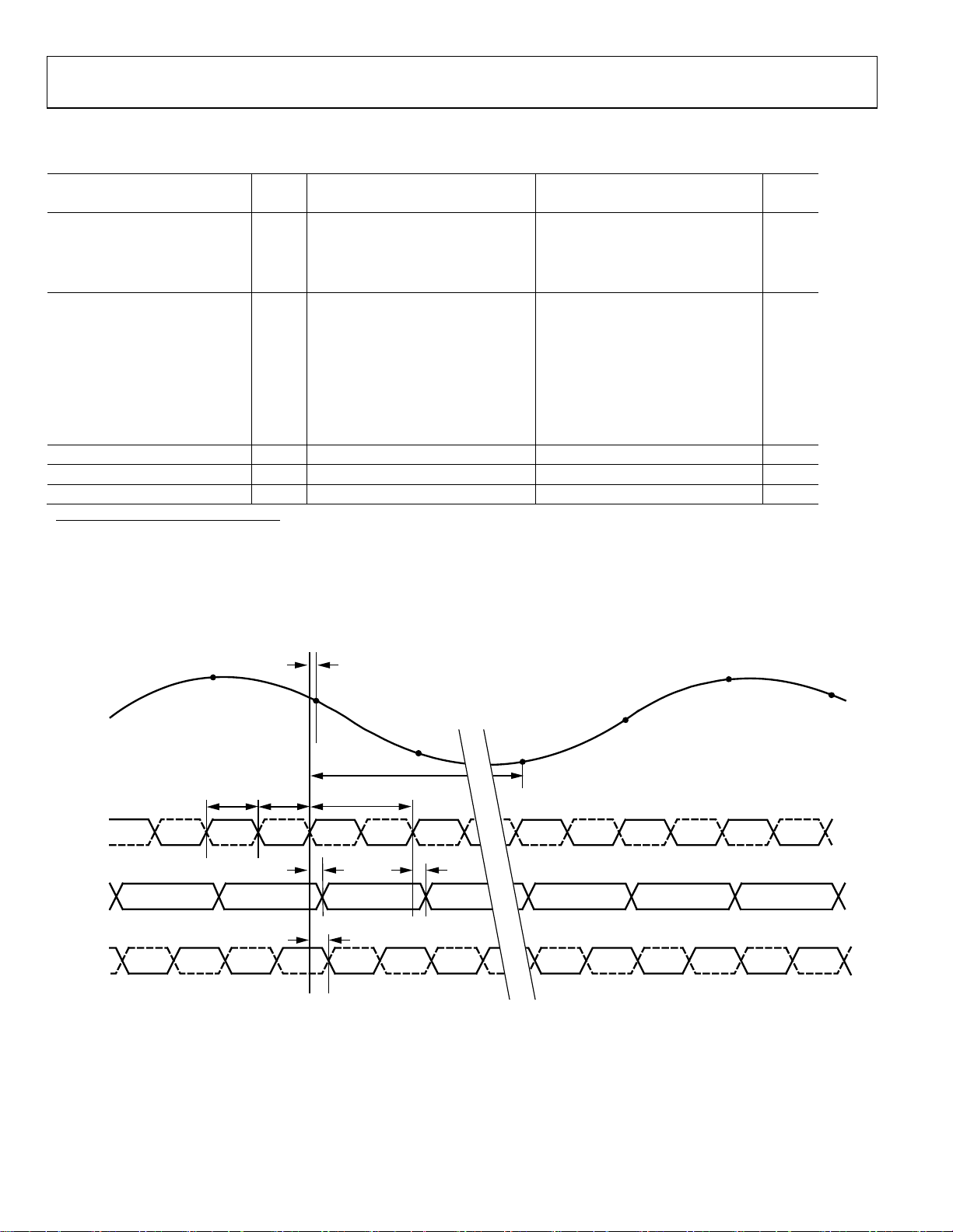
AIN
CLK+
CLK–
DATA
OUT
DCO+
DCO–
N–1
t
A
N
N+L+1
N+1
L CYCLES
t
EH
t
CPD
t
EL
1/f
S
t
PD
N–L
Figure 2. Timing Diagram (L=5 Cycles)
t
V
N-L+1 N N+1 N+2
N+L
N+L+2
N+L+3
Rev. PrA | Page 6 of 21
Preliminary Technical Data AD9211
ABSOLUTE MAXIMUM RATINGS
Parameter Rating
AVDD 2.0 V
DRVDD 2.0V
Analog Inputs –0.5 V to AVDD + 0.5 V
Digital Inputs –0.5 V to DRVDD + 0.5 V
REFIN Inputs –0.5 V to AVDD + 0.5 V
Digital Output Current 20 mA
Operating Temperature –40ºC to +125°C
Storage Temperature –65ºC to +150°C
Maximum Junction
Temperature
Maximum Case Temperature 150°C
θJA 2 TBD°C/W
1Stresses above those listed under Absolute Maximum Ratings may cause
permanent damage to the device. This is a stress rating only; functional
operation of the device at these or any other conditions outside of those
indicated in the operation sections of this specification is not implied.
Exposure to absolute maximum ratings for extended periods may affect
device reliability.
2 Typical θ
with solid ground plane.
= TBD C/W (heat slug soldered) for multilayer board in still air
JA
150°C
1
ESD CAUTION
ESD (electrostatic discharge) sensitive device. Electrostatic charges as high as 4000 V readily accumulate on the
human body and test equipment and can discharge without detection. Although this product features
proprietary ESD protection circuitry, permanent damage may occur on devices subjected to high energy
electrostatic discharges. Therefore, proper ESD precautions are recommended to avoid performance
degradation or loss of functionality.
Rev. PrA | Page 7 of 21

AD9211 Preliminary Technical Data
PIN CONFIGURATIONS AND FUNCTION DESCRIPTIONS
D0+
D0-
DNC
DNC
DCO+
DCO-
DRGND
DRVDD
AVDD
CLK-
CLK+
454944
AVDD
43
42
AVDD
41
AVDD
40
CML
39
AVDD
38
AVDD
37
AVDD
36
VIN-
35
VIN+
34
AVDD
33
AVDD
32
AVDD
31
RBIAS
30
AVDD
29
PDN
27
28
D1-
D1+
D2-
D2+
D3-
D3+
DRVDD
DRGND
D4-
D4+
D5-
D5+
D6-
D6+
DNC
555453
17
181920
524751
56 Lead for
TOP VIEW
(Not to Scale)
56
1
2
3
4
5
6
7
8
9
10
11
12
13
14
Pin 0 (exposed paddle) = AGND
16
15
DNC
50
AD9211
LF-CSP
212622
48
46
25
23
24
D7-
D8-
D9-
D8+
D7+
(MSB) D9+
OVR-
OVR+
DRGND
DRVDD
CSB
SDIO
SCLK
RESET
Figure 3. Pinout
Table 5. PIN FUNCTION DESCRIPTIONS
Pin Number Mnemonic Description
30,32,33,34,37,38,39,41,
AVDD 1.8 V Analog Supply.
42,43,46
7, 24,47 DRVDD 1.8 V Digital Output Supply.
0 AGND1 Analog Ground.
8, 23,48 DRGND1 Digital Output Ground.
35 VIN+ Analog Input—True.
36 VIN– Analog Input—Complement.
40 CML Analog input common mode output pin
44 CLK+ Clock Input—True.
45 CLK– Clock Input—Complement.
31 RBIAS Set Pin for Chip Bias Current. (Place 1% X kohm resistor terminated to ground).
28 RESET Chip Reset ( Active high)
25 SDIO Serial port input/output pin
26 SCLK Serial port clock
27
29
CSB
PWDN
Serial port chip select (Active low)
Chip power down
49 DCO– Data Clock Output—Complement.
50 DCO+ Data Clock Output—True.
51-54 DNC Do not connect
55 D0– D0 Complement Output Bit.
56 D0+ D0 True Output Bit.
1
AGND and DRGND should be tied to a common quiet ground plane.
Rev. PrA | Page 8 of 21

Preliminary Technical Data AD9211
Pin Number Mnemonic Description
1 D1– D1 Complement Output Bit.
2 D1+ D1 True Output Bit.
3 D2– D2 Complement Output Bit.
4 D2+ D2 True Output Bit.
5 D3– D3 Complement Output Bit.
5 D3+ D3 True Output Bit.
9 D4– D4 Complement Output Bit.
10 D4+ D4 True Output Bit.
11 D5– D5 Complement Output Bit.
12 D5+ D5 True Output Bit.
13 D6– D6 Complement Output Bit.
14 D6+ D6 True Output Bit.
15 D7– D7 Complement Output Bit.
16 D7+ D7 True Output Bit.
17 D8– D8 Complement Output Bit.
18 D8+ D8 True Output Bit.
19 D9– D9 Complement Output Bit.
20 D9+ D9 True Output Bit.
21 OTR– Overrange Complement Output Bit.
22 OTR+ Overrange True Output Bit.
Rev. PrA | Page 9 of 21

AD9211 Preliminary Technical Data
TERMINOLOGY
Analog Bandwidth
Full-Scale Input Power
The analog input frequency at which the spectral power of the
fundamental frequency (as determined by the FFT analysis) is
reduced by 3 dB.
Aperture Delay
The delay between the 50% point of the rising edge of the Clock
and the instant at which the analog input is sampled.
Aperture Uncertainty (Jitter)
The sample-to-sample variation in aperture delay.
Crosstalk
Coupling onto one channel being driven by a low level (–40
dBFS) signal when the adjacent interfering channel is driven by
a fullscale signal.
Differential Analog Input Resistance, Differential Analog
Input Capacitance, and Differential Analog Input Impedance
The real and complex impedances measured at each analog
input port. The resistance is measured statically and the
capacitance and differential input impedances are measured
with a network analyzer.
Differential Analog Input Voltage Range
The peak-to-peak differential voltage that must be applied to
the converter to generate a full-scale response. Peak differential
voltage is computed by observing the voltage on a single pin
and subtracting the voltage from the other pin, which is 180°
out of phase. Peak-to-peak differential is computed by rotating
the input’s phase 180° and again taking the peak measurement.
The difference is then computed between both peak
measurements.
Differential Nonlinearity
The deviation of any code width from an ideal 1 LSB step.
Effective Number of Bits (ENOB)
Calculated from the measured SNR based on the equation
−
ENOB
=
MEASURED
76.1 dBSNR
02.6
Expressed in dBm. Computed using the following equation:
⎛
⎜
2
V
FULLSCALE
⎜
=
Power
FULLSCALE
log10
Z
⎜
INPUT
⎜
⎝
001.0
RMS
⎞
⎟
⎟
⎟
⎟
⎠
Gain Error
The difference between the measured and ideal full-scale input
voltage range of the ADC.
Harmonic Distortion, Second
The ratio of the rms signal amplitude to the rms value of the
second harmonic component, reported in dBc.
Harmonic Distortion, Third
The ratio of the rms signal amplitude to the rms value of the
third harmonic component, reported in dBc.
Integral Nonlinearity
The deviation of the transfer function from a reference line
measured in fractions of 1 LSB using a “best straight line”
determined by a least square curve fit.
Minimum Conversion Rate
The Clock rate at which the SNR of the lowest analog signal
frequency drops by no more than 3 dB below the guaranteed
limit.
Maximum Conversion Rate
The Clock rate at which parametric testing is performed.
Output Propagation Delay
The delay between a differential crossing of CLK+ and CLK–
and the time when all output data bits are within valid logic
levels.
Noise (for Any Range within the ADC)
Calculated as follows:
Clock Pulsewidth/Duty Cycle
Pulsewidth high is the minimum amount of time the ENCODE
pulse should be left in Logic 1 state to achieve rated
performance; pulsewidth low is the minimum time the Clock
pulse should be left in low state. At a given clock rate, these
specifications define an acceptable Clock duty cycle.
Rev. PrA | Page 10 of 21
−−
⎛
××=
NOISE
where
ZV
Z is the input impedance, FS is the full scale of the device
for the frequency in question,
input level, and
10001.0
⎜
⎝
SNR is the value of the particular
Signal is the signal level within the ADC
SignalSNRFS
10
⎞
dBFSdBcdBM
⎟
⎠

Preliminary Technical Data AD9211
reported in dB below full scale. This value includes both
thermal and quantization noise.
of the worst third-order intermodulation product; reported in
dBc.
Power Supply Rejection Ratio
The ratio of a change in input offset voltage to a change in
power supply voltage.
Signal-to-Noise-and-Distortion (SINAD)
The ratio of the rms signal amplitude (set 1 dB below full scale)
to the rms value of the sum of all other spectral components,
including harmonics but excluding dc.
Signal-to-Noise Ratio (without Harmonics)
The ratio of the rms signal amplitude (set at 1 dB below full
scale) to the rms value of the sum of all other spectral
components, excluding the first five harmonics and dc.
Spurious-Free Dynamic Range (SFDR)
The ratio of the rms signal amplitude to the rms value of the
peak spurious spectral component. The peak spurious
component may or may not be a harmonic. May be reported in
dBc (i.e., degrades as signal level is lowered) or dBFS (always
related back to converter full scale).
Two-Tone Intermodulation Distortion Rejection
The ratio of the rms value of either input tone to the rms value
Two -Tone SFDR
The ratio of the rms value of either input tone to the rms value
of the peak spurious component. The peak spurious component
may or may not be an IMD product. May be reported in dBc
(i.e., degrades as signal level is lowered) or in dBFS (always
related back to converter full scale).
Worst Other Spur
The ratio of the rms signal amplitude to the rms value of the
worst spurious component (excluding the second and third
harmonic) reported in dBc.
Transi e nt Res p onse T i m e
The time it takes for the ADC to reacquire the analog input
after a transient from 10% above negative full scale to 10%
below positive full scale.
Out-of-Range Recovery Time
The time it takes for the ADC to reacquire the analog input
after a transient from 10% above positive full scale to 10% above
negative full scale, or from 10% below negative full scale to 10%
below positive full scale.
Rev. PrA | Page 11 of 21

AD9211 Preliminary Technical Data
EQUIVALENT CIRCUITS
AVDD
AVDD
CLK+
AVDD
Vcm
AVDD
CLK-
DRVDD
10k10k
V+
Dataout-
V–
V–
Dataout+
V+
Figure 4 Clock Input s
Figure 7. Data Outputs (LVDS Mode)
.
AVDD
VIN+
AVDD
BUF
AVDD
1000 Ω
BUF
1000 Ω
VIN-
BUF
Figure 5. Analog Inputs (VX=~ 1.3V)
AVDD
IN
Figure 6. Logic Inputs
AVDD
Rev. PrA | Page 12 of 21

Preliminary Technical Data AD9211
TYPICAL PERFORMANCE
CHARACTERISTICS
TBD
Rev. PrA | Page 13 of 21

AD9211 Preliminary Technical Data
THEORY OF OPERATION
The AD9211 architecture consists of a front-end sample and
hold amplifier (SHA) followed by a pipelined switched capacitor
ADC. The quantized outputs from each stage are combined into
a final 10-Bit result in the digital correction logic. The pipelined
architecture permits the first stage to operate on a new input
sample, while the remaining stages operate on preceding
samples. Sampling occurs on the rising edge of the clock.
Each stage of the pipeline, excluding the last, consists of a low
resolution flash ADC connected to a switched capacitor DAC
and interstage residue amplifier (MDAC). The residue amplifier
magnifies the difference between the reconstructed DAC output
and the flash input for the next stage in the pipeline. One bit of
redundancy is used in each stage to facilitate digital correction
of flash errors. The last stage simply consists of a flash ADC.
The input stage contains a differential SHA that can be ac- or
dc-coupled in differential or single-ended modes. The outputstaging block aligns the data, carries out the error correction,
and passes the data to the output buffers. The output buffers are
powered from a separate supply, allowing adjustment of the
output voltage swing. During power-down, the output buffers
go into a high impedance state.
ANALOG INPUT AND VOLTAGE REFERENCE
The analog input to the AD9211 is a differential buffer. For
best dynamic performance, the source impedances driving
VIN+ and VIN
settling errors are symmetrical. The analog input is optimized
to provide
the analog inputs be driven differentially. SNR and SINAD
performance degrades significantly if the analog input is driven
with a single-ended signal.
A wideband transformer, such as Mini-Circuits’ ADT1-1WT,
can provide the differential analog inputs for applications that
require a single-ended-to-differential conversion. Both analog
inputs are self-biased by an on-chip resistor divider to a
nominal 1.3 V.
An internal differential voltage reference creates positive and
negative reference voltages that define the 1.25Vp-p fixed span
of the ADC core. This internal voltage reference can be
adjusted by means of SPI control. See SPI control section for
more details.
Differential Input Configurations
Optimum performance is achieved while driving the AD9211
in a differential input configuration. For baseband applications,
the AD8138 differential driver provides excellent performance
and a flexible interface to the ADC. The output common-mode
voltage of the AD8138 is easily set to AVDD/2+0.5V, and the
driver can be configured in a Sallen-Key filter topology to
provide band limiting of the input signal.
–
should be matched such that common mode
superior
wideband performance and requires that
1V p-p
Figure 8. Differential Input Configuration Using the AD8138
0.1
49.9
μ
Ω
499
F
523
Ω
Ω
Ω
499
AD8138
Ω
499
Ω
33
20pF
33
Ω
AVDD
VIN+
AD9211
–
VIN
CML
At input frequencies in the second Nyquist zone and above, the
performance of most amplifiers is not adequate to achieve the
true performance of the AD9211. This is especially true in IF
under-sampling applications where frequencies in the 70 MHz
to 100 MHz range are being sampled. For these applications,
differential transformer coupling is the recommended input
configuration. The signal characteristics must be considered
when selecting a transformer. Most RF transformers saturate at
frequencies below a few MHz, and excessive signal power can
also cause core saturation, which leads to distortion.
In any configuration, the value of the shunt capacitor, C, is
dependent on the input frequency and may need to be reduced
or removed.
Ω
1.25V p-p
Ω
49.9
μF
0.1
Figure 9. Differential Transformer—Coupled Configuration
33
10pF
33
VIN+
AD9211
Ω
VIN
–
Single-Ended Input Configuration
A single-ended input can provide adequate performance in
cost-sensitive applications. In this configuration, SFDR and
distortion performance degrade due to the large input
common-mode swing. However, if the source impedances
on each input are matched, there should be little effect on
SNR performance. Figure 10 details a typical single-ended
input configuration.
05491-004
05491-005
Rev. PrA | Page 14 of 21

Preliminary Technical Data AD9211
1 0 µ F
150Ω
150Ω
0.1uF
0.1uF
CLK+
AD9230
CLK-
VIN+
A D9
VINCML
AVDD
211
AGND
R
1.25Vp-p
Figure 10. Single-Ended Input Configuration using SPI enabled CML function
4 9 . 9
0 . 1 µ F
Ω
0.1uF
PECL
AD9512
CLOCK INPUT CONSIDERATIONS
For optimum performance, the AD9211 the sample clock inputs
(CLK+ and CLK-) should be clocked with a differential signal.
This signal is typically ac-coupled into the CLK+ and CLK- pins
via a transformer or capacitors. These pins are biased internally
and require no additional bias (See Figure X).
AVDD
1.2V
CLK+
2pF 2pF
Figure .Equivalent Clock Input Circuit
Figure X shows one preferred method for clocking the AD9211.
The clock source (low jitter) is converted from single-ended to
differential using an RF transformer. The back-to-back Schottky
diodes across the transformer secondary limit clock excursions
into the AD9211 to approximately 0.8 V p-p differential. This
helps prevent the large voltage swings of the clock from feeding
through to other portions of the AD9211 while preserving the
fast rise and fall times of the signal, which are critical to a low
jitter performance.
CLK-
Figure X. Differential PECL Sample Clock for AD9230/AD9211
CLK+
Clock
Source
Figure X. Transformer Coupled Differential Clock for AD9230/AD9211
AD9230
CLK-
If a low jitter clock is available, another option is to ac-couple a
differential PECL signal to the sample clock input pins as shown
in Figure X. The AD9512 (or same family) from offers excellent
jitter performance.
Rev. PrA | Page 15 of 21

AD9211 Preliminary Technical Data
Clock Input Considerations
Typical high speed ADCs use both clock edges to generate a
variety of internal timing signals, and as a result may be
sensitive to clock duty cycle. Commonly, a 5% tolerance is
required on the clock duty cycle to maintain dynamic
performance
characteristics. The AD9211 contains a DCS (duty cycle
stabilizer) that retimes the non-sampling edge, providing an
internal clock signal with a nominal 50% duty cycle. This allows
a wide range of clock input duty cycles without affecting the
performance of the AD9211. Noise and distortion performance
are nearly flat for a wide range duty cycles with the DCS on.
The duty cycle stabilizer uses a delay-locked loop (DLL) to
create the non-sampling edge. As a result, any changes to the
sampling frequency require approximately TBD clock cycles to
allow the DLL to acquire and lock to the new rate.
Jitter Considerations
High speed, high resolution ADCs are sensitive to the quality of
the clock input. The degradation in SNR at a given input
frequency (f
) due only to aperture jitter (tJ) can be
INPUT
calculated by
AD9211. Power supplies for clock drivers should be separated
from the ADC output driver supplies to avoid modulating the
clock signal with digital noise. Low jitter, crystal-controlled
oscillators make the best clock sources. If the clock is generated
from another type of source (by gating, dividing, or other
methods), it should be retimed by the original clock at the last
step.
POWER DISSIPATION AND POWER DOWN MODE
As shown in Figure 12 and Figure 14, the power dissipated by
the AD9211 is proportional to its sample rate. The digital power
dissipation does not vary much because it is determined
primarily by the DRVDD supply and bias current of the LVDS
output drivers.
π
⎡
=
20logSNR
INPUT
⎢
2
⎣
⎤
×
tf
J
⎥
⎦
In the equation, the rms aperture jitter represents the rootmean square of all jitter sources, which include the clock input,
analog input signal, and ADC aperture jitter specification. IF
under-sampling applications are particularly sensitive to jitter,
see Figure 11.
75
0.2ps
0.5ps
1.0ps
1.5ps
2.0ps
2.5ps
3.0ps
100010010
SNR (dBc)
70
65
60
55
50
45
40
1
INPUT FREQUENCY (MHz)
Figure 12. AD9211-170, Supply Current vs. f
Figure 13. AD9211-200, Supply Current vs. f
for fIN = 10.3 MHz
SAMPLE
for fIN = 10.3 MHz
SAMPLE
Figure 11. SNR vs. Input Frequency and Jitter
The clock input should be treated as an analog signal in cases
where aperture jitter may affect the dynamic range of the
Rev. PrA | Page 16 of 21

Preliminary Technical Data AD9211
The format of the output data is offset binary. An example of
the output coding format can be found in Table 7.
Table 7. Digital Output Coding
Figure 14. AD9211-250, Supply Current vs. f
for fIN = 10.3 MHz
SAMPLE
By asserting the PDWN pin high, the AD9211 is placed in
standby mode. In this state, the ADC typically dissipates
1 mW even if the CLK and analog inputs are static. During
standby, the output drivers are placed in a high impedance state.
Reasserting the PDWN pin low returns the AD9211 into its
normal operational mode.
An additional stand by mode is supported by means of varying
the clock input. When the clock rate falls below 20MHz, the
AD9211 will assume a standby state. In this case, the biasing
network and internal reference remain on but digital circuitry is
powered down. Upon reactivating the clock, the AD9211 will
resume normal operation after allowing for the pipeline latency.
(VIN+) − (VIN−),
Input Span =
Code
1.252 V p-p (V)
1024 1.000 11 1111 1111
512 0 10 0000 0000
511 −0.000488 01 1111 1111
0 −1.00 00 0000 0000
As detailed in Interfacing to ADC SPI, the data format can be
selected for either offset binary or twos complement, or Gray
code (SPI access only).
Out-of-Range (OTR)
An out-of-range condition exists when the analog input voltage
is beyond the input range of the ADC. OTR is a digital output
that is updated along with the data output corresponding to the
particular sampled input voltage. Thus, OTR has the same
pipeline latency as the digital data. OTR is low when the analog
input voltage is within the analog input range and high when
the analog input voltage exceeds the input range as shown in
Figure 15. OTR will remain high until the analog input returns
to within the input range and another conversion is completed.
By logically AND-ing OTR with the MSB and its complement,
over-range high or under-range low conditions can be detected.
Digital Output
Offset Binary
(D9 ... D0)
DIGITAL OUTPUTS
The AD9228’s differential outputs conform to the ANSI-644
LVDS standard on default power up. The LVDS driver current
is derived on-chip and sets the output current at each output
equal to a nominal 3.5 mA. A 100 Ω differential termination
resistor placed at the LVDS receiver inputs results in a nominal
350 mV swing at the receiver.
The AD9211’s LVDS outputs facilitate interfacing with LVDS
receivers in custom ASICs and FPGAs that have LVDS capability for superior switching performance in noisy environments. Single point-to-point net topologies are recommended
with a 100 Ω termination resistor placed as close to the receiver
as possible. It is recommended to keep the trace length no
longer than 12 inches and to keep differential output traces
close together and at equal lengths.
Figure 15. OTR Relation to Input Voltage and Output Data for
AD9230/AD9211
TIMING
The AD9211 provides latched data outputs with a pipeline delay
of five clock cycles. Data outputs are available one propagation
delay (t
) after the rising edge of the clock signal.
PD
Rev. PrA | Page 17 of 21

AD9211 Preliminary Technical Data
The length of the output data lines and loads placed on them
should be minimized to reduce transients within the AD9211.
These transients can degrade the converter’s dynamic performance.
The AD9211 also provides data clock output (DCO) intended for
capturing the data in an external register. The data outputs are
valid on the rising edge of DCO.
The lowest typical conversion rate of the AD9211 is 40 MSPS.
At clock rates below 1 MSPS, the AD9211 will assume standby
mode.
Spec
Name
tDS Setup time between data and rising edge of SCLK
tDH Hold time between data and rising edge of SCLK
t
Period of the clock
CLK
tS Setup time between CSB and SCLK
tH Hold time between CSB and SCLK
Meaning
RBIAS
The AD9211 requires the user to place a 10KΩ resistor between
the RBIAS pin and ground. This resister should have a 1%
tolerance, and is used to set the master current reference of the
ADC core.
AD9211 CONFIGURATION USING THE SPI
The AD9211 serial port interface allows the user to configure
the converter for specific functions or operations through a
structured register space inside the ADC. This gives the user
added flexibility to customize device operation depending on
the application. Addresses are accessed (programmed or read
back) serially in one-byte words. Each byte may be further
divided down into fields which are documented in the Memory
Map Section below.
There are three pins that define the serial port interface or SPI
to this particular ADC. They are the SPI SCLK / DFS, SPI SDIO
/ DCS, and CSB pins. The SCLK/DFS (serial clock) is used to
synchronize the read and write data presented the ADC.. The
SDIO / DCS (serial data input/output) is a dual purpose pin
that allows data to be sent and read from the internal ADC
memory map registers. The CSB or chip select bar is an active
low control that enables or disables the read and write cycles.
See Table X.
Table X. Serial Port Pins
Pin Function
SCLK
SDIO
CSB
RESET
SCLK (Serial Clock) is the serial shift clock in. SCLK is
used to synchronize serial interface reads and writes.
SDIO (Serial Data Input/Output) is a dual purpose pin.
The typical role for this pin is an input and output
depending on the instruction being sent and the
relative position in the timing frame.
CSB (Chip Select Bar) is active low controls that gates
the read and write cycles.
Master device reset. When asserted, device assumes
default settings.
tHI
tLO
Minimum period that SCLK should be in a logic high
state
Minimum period that SCLK should be in a logic low
state
During an instruction phase a 16bit instruction is transmitted.
Data then follows the instruction phase and is determined by
the W0 and W1 bits which is 1 or more bytes of data. All data is
composed of 8bit words. The first bit of each individual byte of
serial data indicates whether this is a read or write command.
This allows the serial data input/output (SDIO) pin to change
direction from an input to an output.
Data may be sent in MSB or in LSB first mode. MSB first is
default on power up and may be changed by changing the
configuration register. For more information about this feature
and others see SPI Doc at www.analog.com.
The falling edge of the CSB in conjunction with the rising edge
of the SCLK determines the start of the framing. An example of
the serial timing and its definitions can be found in Figure X
and Table X. Table X. SPI Timing Diagram specifications
Rev. PrA | Page 18 of 21

Preliminary Technical Data AD9211
HARDWARE INTERFACE
The pins described in Table X comprise the physical interface
between the user’s programming device and the serial port of
the AD9211. All serial pins are inputs, which is an open-drain
output and should be tied to an external pull-up or pull-down
resistor (suggested value 10 kΩ).
This interface is flexible enough to be controlled by either
PROMS or PIC mirocontrollers as well. This provides the user
to use an alternate method to program the ADC other than a
SPI controller.
If the user chooses to not use the SPI interface, some pins serve
a dual function and are associated with a specific function when
strapped externally to AVDD or ground during device power
on. The section below describes the strappable functions
supported on the AD9211. AD9211
CONFIGURATION WITHOUT THE SPI
In applications that do not interface to the SPI control registers,
the SPI SDIO / DCS and SPI SCLK / DFS pins can alternately
serve as stand alone CMOS compatible control pins When the
device is powered up, it is assumed that the user intends to use
the pins as static control lines for the duty cycle stabilizer. In
this mode the SPI CSB chip select should be connected to
AVDD, which will disable the serial port interface.
Table 6. Mode Selection
Pin External
Voltage
AVDD Duty Cycle Stabilizer Enabled SPI SDIO / DCS
AGND Duty Cycle Stabilizer Disabled
AVDD 2’s Complement Enabled SPI SCLK / DFS
AGND Offset Binary Enabled
Configuration
READING THE MEMORY MAP TABLE
Each row in the memory map table has eight address locations.
The memory map is roughly divided into four sections: chip
configuration register map (Address 0x00 to Address 0x02),
device index and transfer register map (Address 0x04 to
Address 0x05, and Address 0xFF), global ADC function register
map (Address 0x08 to Address 0x09), and flexible ADC
functions register map (Address 0x0B to Address 0x25). The
flexible ADC functions register map is product specific.
Starting from the right hand column, the memory map register
in Table X documents the default hex value for each hex address
shown. The column with the heading Byte 7 (MSB) is the start
of the default hex value giving. For example, hex address 0x14,
flex_output_phase has a hex default value of 00h. This means
Bit 3 = 0, Bit 2 = 0, Bit 1 = 1, and Bit 0 = 1 or 0011 in binary.
This setting is the default output clock or DCO phase adjust
option. The default value adjusts the DCO phase 90deg relative
to the Nominal DCO edge and 180deg relative to the data edge.
For more information on this function and others consult the
SPI Doc at www.analog.com.
OPEN LOCATIONS
All locations marked as “open” are currently not supported for
this particular device. When required, these locations should be
written with 0s. Writing to these locations is required only when
part of an address location is open (for example, Address 0x14).
If the whole address location is open (for example, Address
0x13), then this address location does not need to be written.
DEFAULT VALUES
Coming out of reset, some of the address locations (but not all)
are loaded with default values. The default values for the
registers are given in the Table X.
LOGIC LEVELS
An explanation of various registers, “bit is set” is synonymous
with “bit is set to Logic 1” or “writing Logic 1 for the bit.”
Similarly “clear a bit” is synonymous with “bit is set to Logic 0”
or “writing Logic 0 for the bit.”
Figure X. Serial Port Interface Timing Diagram
Rev. PrA | Page 19 of 21

AD9211 Preliminary Technical Data
Table X. AD9211 Device Configuration Register Memory Map
.
Rev. PrA | Page 20 of 21

Preliminary Technical Data AD9211
OUTLINE DIMENSIONS
a
1.00
0.85
0.80
SEATING
PLANE
12° MAX
BSC SQ
PIN 1
INDICATOR
56-Lead Lea d Frame Chi p Scale Package [LFCSP _V Q]
8.00
TOP
VIEW
0.50 BSC
COMPLIANT TO JEDEC STANDARDS MO-220-VL LD-2
8 x 8 mm Body, Very Thin Qu ad
Dimensions shown in millimeters
0.80 MAX
0.65 TYP
7.75
BSC SQ
0.20 REF
(CP-56-2)
0.60 MAX
0.05 MAX
0.02 NOM
0.50
0.40
0.30
COPLANARITY
0.08
43
42
29
28
0.60 MAX
EXPOSED
PAD
(BOTTOM VIEW)
6.50
REF
0.30
0.23
0.18
PIN 1
56
INDICATOR
1
4.45
4.30 SQ
4.15
14
15
0.30 MIN
112805-0
Figure 16. Mechanical Drawing (Subject to change)
ORDERING GUIDE
Temperature
Model
AD9211BCPZ-1701 −40°C to +85°C 56-Lead Lead Frame Chip Scale Package (LFCSP-VQ) CP-56
AD9211BCPZ-2001 −40°C to +85°C 56-Lead Lead Frame Chip Scale Package (LFCSP-VQ) CP-56
AD9211BCPZ-2501 −40°C to +85°C 56-Lead Lead Frame Chip Scale Package (LFCSP-VQ) CP-56
AD9211-250EB 25°C LVDS Evaluation Board with AD9211BCPZ-250
AD9211-200EB 25°C LVDS Evaluation Board with AD9211BCPZ-200
AD9211-170EB 25°C LVDS Evaluation Board with AD9211BCPZ-170
1
Z=Pb-free part
© 2006 Analog Devices, Inc. All rights reserved. Trademarks and
registered trademarks are the property of their respective companies.
Printed in the U.S.A.
PR06041-0-3/06(PrA)
Range Package Description Package Option
Rev. PrA | Page 21 of 21
 Loading...