Analog Devices AD9203 b Datasheet
10-Bit, 40 MSPS, 3 V, 74 mW
FEATURES
CMOS 10-Bit, 40 MSPS sampling A/D converter
Power dissipation: 74 mW (3 V supply, 40 MSPS)
17 mW (3 V supply, 5 MSPS)
Operation between 2.7 V and 3.6 V supply
Differential nonlinearity: −0.25 LSB
Power-down (standby) mode, 0.65 mW
ENOB: 9.55 @ f
Out-of-range indicator
Adjustable on-chip voltage reference
IF undersampling up to f
Input range: 1 V to 2 V p-p differential or single-ended
Adjustable power consumption
Internal clamp circuit
APPLICATIONS
CCD imaging
Video
Portable instrumentation
IF and baseband communications
Cable modems
Medical ultrasound
GENERAL DESCRIPTION
The AD9203 is a monolithic low power, single supply, 10-bit,
40 MSPS analog-to-digital converter, with an on-chip voltage
reference. The AD9203 uses a multistage differential pipeline
architecture and guarantees no missing codes over the full
operating temperature range. Its input range may be adjusted
between 1 V and 2 V p-p.
The AD9203 has an onboard programmable reference. An
external reference can also be chosen to suit the dc accuracy
and temperature drift requirements of an application.
An external resistor can be used to reduce power consumption
when operating at lower sampling rates. This yields power
savings for users who do not require the maximum sample rate.
This feature is especially useful at sample rates far below 40
MSPS. Excellent performance is still achieved at reduced power.
For example, 9.7 ENOB performance may be realized with only
17 mW of power, using a 5 MHz clock.
A single clock input is used to control all internal conversion
cycles. The digital output data is presented in straight binary or
twos complementary output format by using the DFS pin. An
Rev. B
Information furnished by Analog Devices is believed to be accurate and reliable.
However, no responsibility is assumed by Analog Devices for its use, nor for any
infringements of patents or other rights of third parties that may result from its use.
Specifications subject to change without notice. No license is granted by implication
or otherwise under any patent or patent rights of Analog Devices. Trademarks and
registered trademarks are the property of their respective owners.
= 20 MHz
IN
= 130 MHz
IN
A/D Converter
AD9203
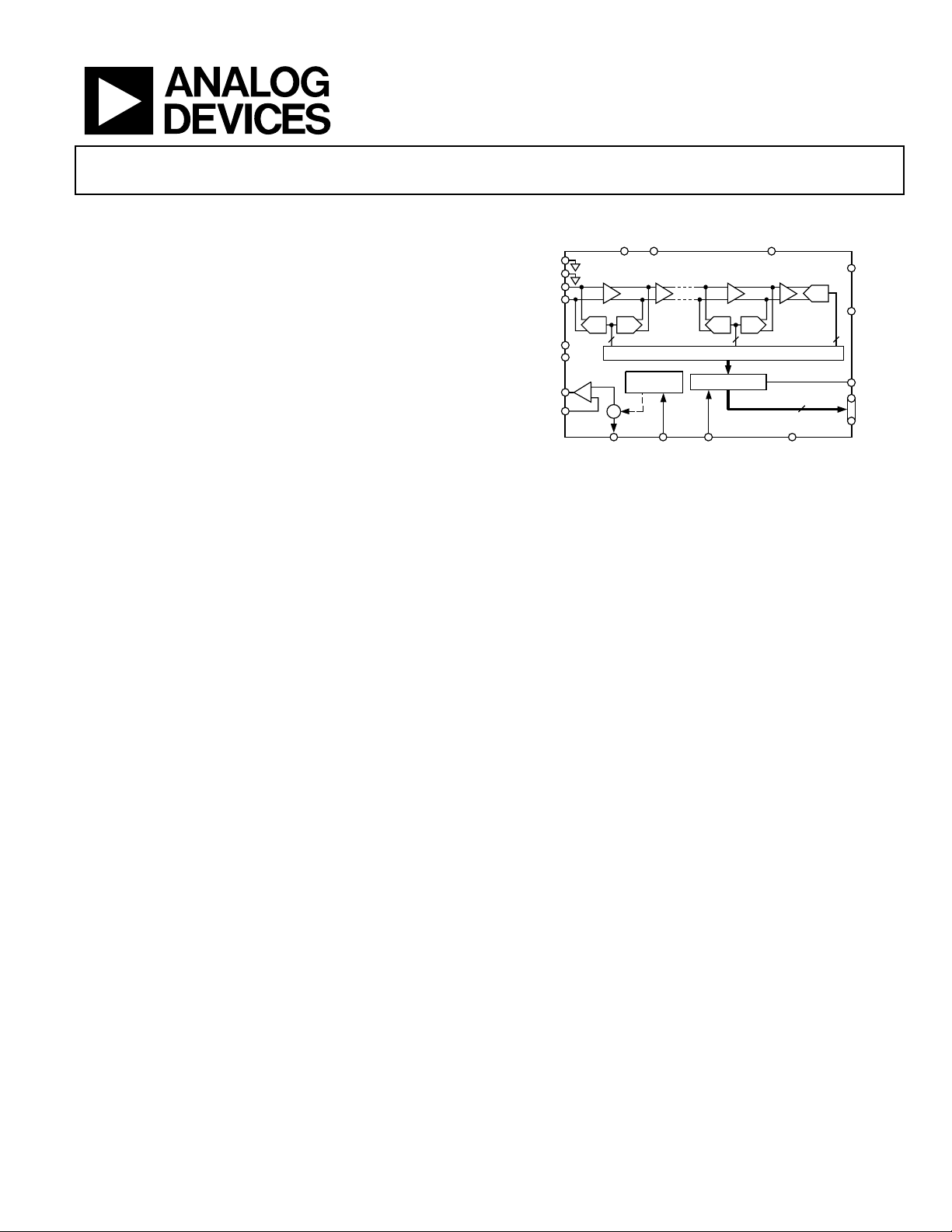
FUNCTIONAL BLOCK DIAGRAM
CLK AVDD DRVDD
CLAMP
CLAMPIN
AINP
AINN
REFTF
REFBF
VREF
REFSENSE
SHA GAIN
A/D D/A
+
–
0.5V
BANDGAP
REFERENCE
SHA GAIN
A/D D/A
CORRECTION LOGIC
OUTPUT BUFFERS
Figure 1.
out-of-range signal (OTR) indicates an overflow condition that
can be used with the most significant bit to determine over- or
underrange.
The AD9203 can operate with a supply range from 2.7 V to 3.6
V, an attractive option for low power operation in high-speed
portable applications.
The AD9203 is specified over industrial (−40°C to +85°C)
temperature ranges and is available in a 28-lead TSSOP package.
PRODUCT HIGHLIGHTS
Low Power—The AD9203 consumes 74 mW on a 3 V supply
operating at 40 MSPS. In standby mode, power is reduced to
0.65 mW.
High Performance—Maintains better than 9.55 ENOB at 40
MSPS input signal from dc to Nyquist.
Ver y Sm al l Pa c ka g e—The AD9203 is available in a 28-lead
TSSOP.
Programmable Power—The AD9203 power can be further
reduced by using an external resistor at lower sample rates.
Built-In Clamp Function—Allows dc restoration of video
signals.
One Technology Way, P.O. Box 9106, Norwood, MA 02062-9106, U.S.A.
Tel: 781.329.4700
Fax: 781.326.8703 © 2004 Analog Devices, Inc. All rights reserved.
www.analog.com
AD9203
10
DRVSSDFSPWRCONAVSS
A/D
STBY
3-STATE
OTR
D9 (MSB)
D0 (LSB)
00573-001

AD9203
TABLE OF CONTENTS
Specifications..................................................................................... 3
Driving the Analog Input .......................................................... 13
Absolute Maximum Ratings............................................................ 5
Thermal Characteristics .............................................................. 5
ESD Caution.................................................................................. 5
Pin Configuration and Function Descriptions............................. 6
Te r mi n ol o g y ...................................................................................... 7
Typical Performance Characteristics............................................. 8
Operations .......................................................................................11
Theory of Operation ..................................................................11
Operational Modes..................................................................... 11
Input and Reference Overview ................................................. 12
Internal Reference Connection ................................................ 12
External Reference Operation .................................................. 13
Clamp Operation........................................................................ 13
REVISION HISTORY
Op Amp Selection Guide .......................................................... 14
Differential Mode of Operation ............................................... 15
Power Control ............................................................................. 16
Interfacing to 5 V Systems ........................................................ 16
Clock Input and Considerations .............................................. 16
Digital Inputs and Outputs ....................................................... 16
Applications..................................................................................... 18
Direct IF Down Conversion ..................................................... 18
Ultrasound Applications ........................................................... 19
Evaluation Board ............................................................................ 20
Outline Dimensions ....................................................................... 25
Ordering Guide .......................................................................... 25
8/04—Data sheet changed from Rev. A to Rev. B
Changes to Table 5.......................................................................... 16
4/01—Data sheet changed from Rev. 0 to Rev. A
Updated Format ..................................................................Universal
Changes to TPC 2............................................................................. 8
Added Figures 41 to 46.................................................................. 23
7/99—Revision 0: Initial Version
Rev. B | Page 2 of 28

AD9203
SPECIFICATIONS
AVDD = 3 V, DRVDD = 3 V, FS = 40 MSPS, input span from 0.5 V to 2.5 V, internal 1 V reference, PWRCON = AVDD, 50% clock duty
MIN
to T
cycle, T
Table 1.
Parameter Symbol Min Typ Max Unit Conditions
RESOLUTION 10 Bits
MAX CONVERSION RATE FS 40 MSPS
PIPELINE DELAY 5.5
DC ACCURACY
Differential Nonlinearity DNL ± 0.25 ± 0.7 LSB
Integral Nonlinearity INL ± 0.65 ± 1.4 LSB
Offset Error E
Gain Error EFS ± 0.7 ± 4.0 % FSR
ANALOG INPUT
Input Voltage Range AIN 1 2 V p-p
Input Capacitance C
Aperture Delay T
Aperture Uncertainty (Jitter) T
Input Bandwidth (–3 dB) BW 390 MHz
Input Referred Noise 0.3 mV Switched, Single-Ended
INTERNAL REFERENCE
Output Voltage (0.5 V Mode) VREF 0.5 V REFSENSE = VREF
Output Voltage (1 V Mode) VREF 1 V REFSENSE = GND
Output Voltage Tolerance (1 V Mode) ± 5 ± 30 mV
Load Regulation 0.65 1.2 mV 1.0 mA Load
POWER SUPPLY
Operating Voltage AVDD 2.7 3.0 3.6 V
DRVDD 2.7 3.0 3.6 V
Analog Supply Current IAVDD 20.1 22.0 mA
Digital Supply Current IDRVDD 4.4 6.0 mA fIN= 4.8 MHz, Output Bus Load = 10pF
9.5 14.0 mA fIN= 20 MHz, Output Bus Load = 20 pF
Power Consumption 74 84.0 mW fIN= 4.8 MHz, Output Bus Load = 10pF
88.8 108.0 mW fIN= 20 MHz, Output Bus Load = 20 pF
Power-Down P
Power Supply Rejection Ratio PSRR 0.04 ± 0.25 % FS
DYNAMIC PERFORMANCE (AIN = 0.5 dBFS)
Signal-to-Noise and Distortion1 SINAD
f = 4.8 MHz 59.7 dB
f = 20 MHz 57.2 59.3 dB
Effective Bits ENOB
f = 4.8 MHz1 9.6 Bits
f = 20 MHz 9.2 9.55 Bits
Signal-to-Noise Ratio SNR
f = 4.8 MHz1 60.0 dB
f = 20 MHz 57.5 59.5 dB
Total Harmonic Distortion THD
f = 4.8MHz −76.0 dB
f = 20 MHz −74.0 −65.0 dB
Spurious-Free Dynamic Range SFDR
f = 4.8 MHz
f = 20 MHz 67.8 78 dB
unless otherwise noted.
MAX
1
Clock
Cycles
ZS
IN
AP
AJ
D
80 dB
± 0.6 ± 2.8 % FSR
1.4 pF
2.0 ns
1.2 ps rms
0.65 1.2 mW
Rev. B | Page 3 of 28
AD9203
A
Parameter Symbol Min Typ Max Unit Conditions
Two-Tone Intermodulation Distortion IMD 68 dB f = 44.49 MHz and 45.52 MHz
Differential Phase DP 0.2 Degree NTSC 40 IRE Ramp
Differential Gain DG 0.3 %
DIGITAL INPUTS
High Input Voltage V
Low Input Voltage V
IH
IL
2.0 V
0.4 V
Clock Pulse Width High 11.25 ns
Clock Pulse Width Low 11.25 ns
Clock Period2 25 ns
DIGITAL OUTPUTS
High-Z Leakage I
Data Valid Delay t
Data Enable Delay t
Data High-Z Delay t
OZ
OD
DEN
DHZ
± 5.0 µA Output = 0 to DRVDD
5 ns CL= 20 pF
6 ns CL= 20 pF
6 ns CL= 20 pF
LOGIC OUTPUT (with DRVDD = 3 V)
High Level Output Voltage (IOH = 50 µA) V
OH
2.95 V
High Level Output Voltage (IOH = 0.5 mA) VOH 2.80 V
Low Level Output Voltage (IOL= 1.6 mA) VOL 0.3 V
Low Level Output Voltage (IOL= 50 µA) V
OL
0.05 V
1
Differential Input (2 V p-p).
2
The AD9203 will convert at clock rates as low as 20 kHz.
N+1
NALOG
INPUT
N
N–1
N+2
N+3
N+4
N+5
N+6
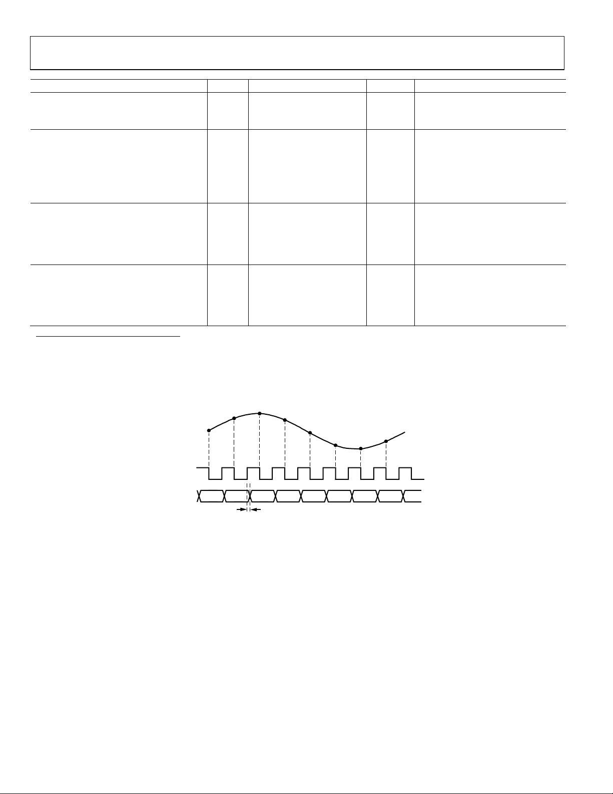
CLOCK
DATA
N–7 N–6 N–5 N–4
OUT
T
= 3ns MIN
OD
N–3 N–2 N–1 N N+1
7ns MAX
(C
= 20pF)
LOAD
00573-002
Figure 2. Timing Diagram
Rev. B | Page 4 of 28
ABSOLUTE MAXIMUM RATINGS
Table 2.
With
Parameter
AVDD AVSS –0.3 +3.9 V
DRVDD DRVSS –0.3 +3.9 V
AVSS DRVSS –0.3 +0.3 V
AVDD DRVDD –3.9 +3.9 V
REFCOM AVSS –0.3 +0.3 V
CLK AVSS –0.3 AVDD + 0.3 V
Digital Outputs DRVSS –0.3 DRVDD + 0.3 V
AINP AINN
VREF AVSS –0.3 AVDD + 0.3 V
REFSENSE AVSS –0.3 AVDD + 0.3 V
REFTF, REFBF AVSS –0.3 AVDD + 0.3 V
STBY AVSS –0.3 AVDD + 0.3 V
CLAMP AVSS –0.3 AVDD + 0.3 V
CLAMPIN AVSS –0.3 AVDD + 0.3 V
PWRCON AVSS –0.3 AVDD + 0.3 V
DFS AVSS –0.3 AVDD + 0.3 V
3-STATE AVSS –0.3 AVDD + 0.3 V
Junction
Temperature
Storage
Temperature
Lead
Temperature
(10 s)
Respect to Min Max Unit
AVSS
–0.3
150 °C
–65 +150 °C
300 °C
AVDD + 0.3 V
AD9203
Stresses above those listed under Absolute Maximum Ratings
may cause permanent damage to the device. This is a stress
rating only; functional operation of the device at these or any
other conditions above those indicated in the operational
sections of this specification is not implied. Exposure to
absolute maximum ratings for extended periods may affect
device reliability.
THERMAL CHARACTERISTICS
28-Lead TSSOP
J
= 97.9°C/W
A
= 14.0°C/W
J
C
ESD CAUTION
ESD (electrostatic discharge) sensitive device. Electrostatic charges as high as 4000 V readily accumulate on
the human body and test equipment and can discharge without detection. Although this product features
proprietary ESD protection circuitry, permanent damage may occur on devices subjected to high energy
electrostatic discharges. Therefore, proper ESD precautions are recommended to avoid performance
degradation or loss of functionality.
Rev. B | Page 5 of 28
AD9203
PIN CONFIGURATION AND FUNCTION DESCRIPTIONS
DRVSS
1
2
DRVDD
D1
D2
D3
D4
D5
D6
D7
D8
OTR
DFS
3
4
5
6
AD9203
TOP VIEW
7
(Not to Scale)
8
9
10
11
12
13
14
(LSB) D0
(MSB) D9
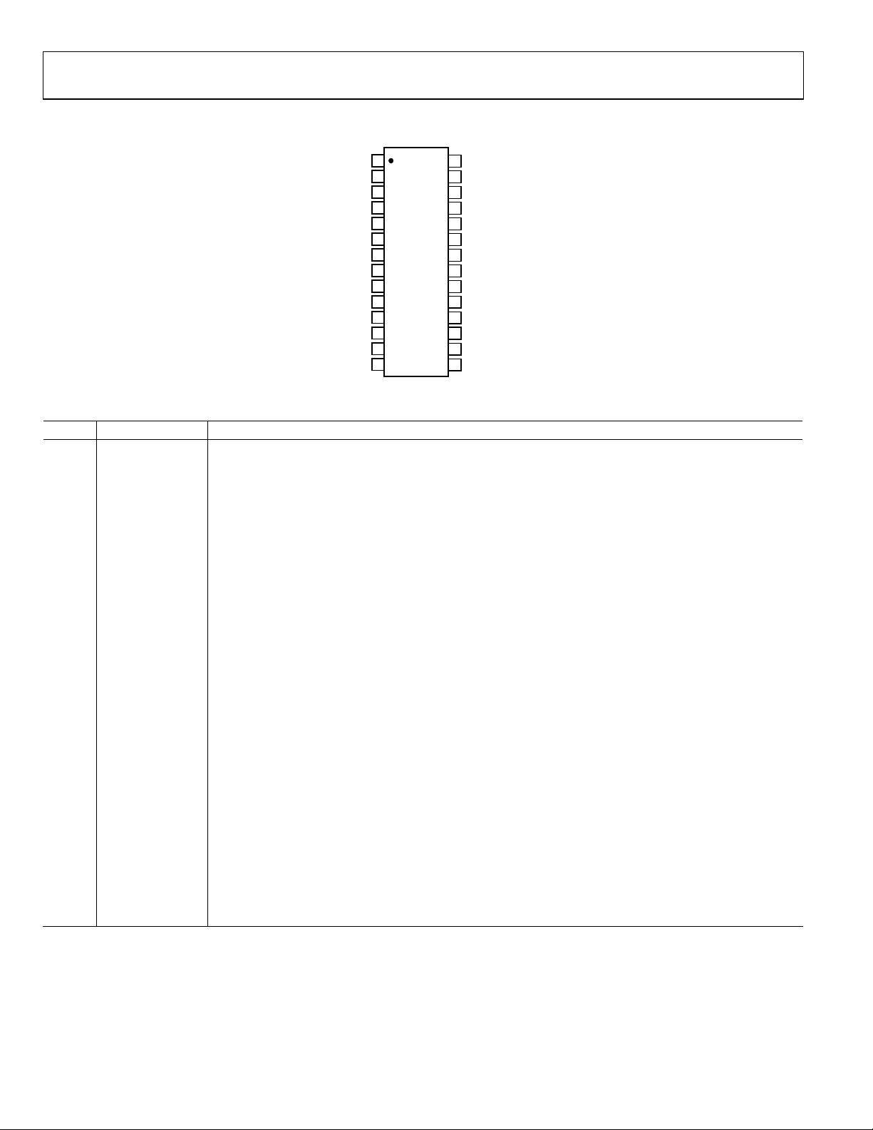
Figure 3. Pin Configuration
Table 3. Pin Function Descriptions
Pin Name Description
1 DRVSS Digital Ground.
2 DRVDD Digital Supply.
3 D0 Bit 0, Least Significant Bit.
4 D1 Bit 1.
5 D2 Bit 2.
6 D3 Bit 3.
7 D4 Bit 4.
8 D5 Bit 5.
9 D6 Bit 6.
10 D7 Bit 7.
11 D8 Bit 8.
12 D9 Bit 9, Most Significant Bit.
13 OTR Out-of-Range Indicator.
14 DFS Data Format Select HI: Twos Complement; LO: Straight Binary.
15 CLK Clock Input.
16 3-STATE HI: High Impedance State Output; LO: Active Digital Output Drives.
17 STBY HI: Power-Down Mode; LO: Normal Operation.
18 REFSENSE Reference Select.
19 CLAMP HI: Enable Clamp; LO: Open Clamp.
20 CLAMPIN Clamp Signal Input.
21 PWRCON Power Control Input.
22 REFTF Top Reference Decoupling.
23 VREF Reference In/Out.
24 REFBF Bottom Reference Decoupling.
25 AINP Noninverting Analog Input.
26 AINN Inverting Analog Input.
27 AVSS Analog Ground.
28 AVDD Analog Supply.
AVDD
28
AVSS
27
AINN
26
AINP
25
24
REFBF
VREF
23
REFTF
22
PWRCON
21
CLAMPIN
20
CLAMP
19
REFSENSE
18
STBY
17
3-STATE
16
CLK
15
00573-003
Rev. B | Page 6 of 28

TERMINOLOGY
Integral Nonlinearity Error (INL)
Linearity error refers to the deviation of each individual code
from a line drawn from negative full scale through positive full
scale. The point used as negative full scale occurs 1/2 LSB
before the first code transition. Positive full scale is defined as a
level 1 1/2 LSB beyond the last code transition. The deviation is
measured from the middle of each particular code to the true
straight line.
Differential Nonlinearity Error (DNL, No Missing Codes)
An ideal ADC exhibits code transitions that are exactly 1 LSB
apart. DNL is the deviation from this ideal value. Guaranteed
no missing codes to 10-bit resolution indicates that all 1024
codes respectively, must be present over all operating ranges.
Signal-To-Noise and Distortion (S/N+D, SINAD) Ratio
S/N+D is the ratio of the rms value of the measured input signal
to the rms sum of all other spectral components below the
Nyquist frequency, including harmonics but excluding dc. The
value for S/N+D is expressed in decibels.
Effective Number of Bits (ENOB)
For a sine wave, SINAD can be expressed in terms of the
number of bits. Using the following formula,
N = (SINAD – 1.76)/6.02
it is possible to get a measure of performance expressed as N,
the effective number of bits.
Thus, effective number of bits for a device for sine wave inputs
at a given input frequency can be calculated directly from its
measured SINAD.
Total Harmonic Distortion (THD)
THD is the ratio of the rms sum of the first six harmonic
components to the rms value of the measured input signal and
is expressed as a percentage or in decibels.
AD9203
Signal-To-Noise Ratio (SNR)
SNR is the ratio of the rms value of the measured input signal to
the rms sum of all other spectral components below the Nyquist
frequency, excluding harmonics and dc. The value for SNR is
expressed in decibels.
Spurious-Free Dynamic Range (SFDR)
The difference in dB between the rms amplitude of the input
signal and the peak spurious signal.
Offset Error
First transition should occur for an analog value 1/2 LSB above
negative full scale. Offset error is defined as the deviation of the
actual transition from that point.
Gain Error
The first code transition should occur at an analog value 1/2
LSB above negative full scale. The last transition should occur
for an analog value 1 1/2 LSB below the positive full scale. Gain
error is the deviation of the actual difference between first and
last code transitions and the ideal difference between first and
last code transitions.
Power Supply Rejection
The specification shows the maximum change in full scale from
the value with the supply at the minimum limit to the value
with the supply at its maximum limit.
Aperture Jitter
Aperture jitter is the variation in aperture delay for successive
samples and is manifested as noise on the input to the A/D.
Aperture Delay
Aperture delay is a measure of the sample-and-hold amplifier
(SHA) performance and is measured from the rising edge of the
clock input to when the input signal is held for conversion.
Pipeline Delay (Latency)
The number of clock cycles between conversion initiation and
the associated output data being made available. New output
data is provided on every rising edge.
Rev. B | Page 7 of 28
AD9203
TYPICAL PERFORMANCE CHARACTERISTICS
AVDD = 3 V, DRVDD = 3 V, FS = 40 MSPS, 1 V Internal Reference, PWRCON = AVDD, 50% Duty Cycle, unless otherwise noted.
61
59
57
55
53
SNR (dB)
51
49
47
0 20 40 60 80 100 120
2V SINGLE-ENDED INPUT
2V DIFFERENTIAL INPUT
1V DIFFERENTIAL INPUT
1V SINGLE-ENDED INPUT
INPUT FREQUENCY (MHz)
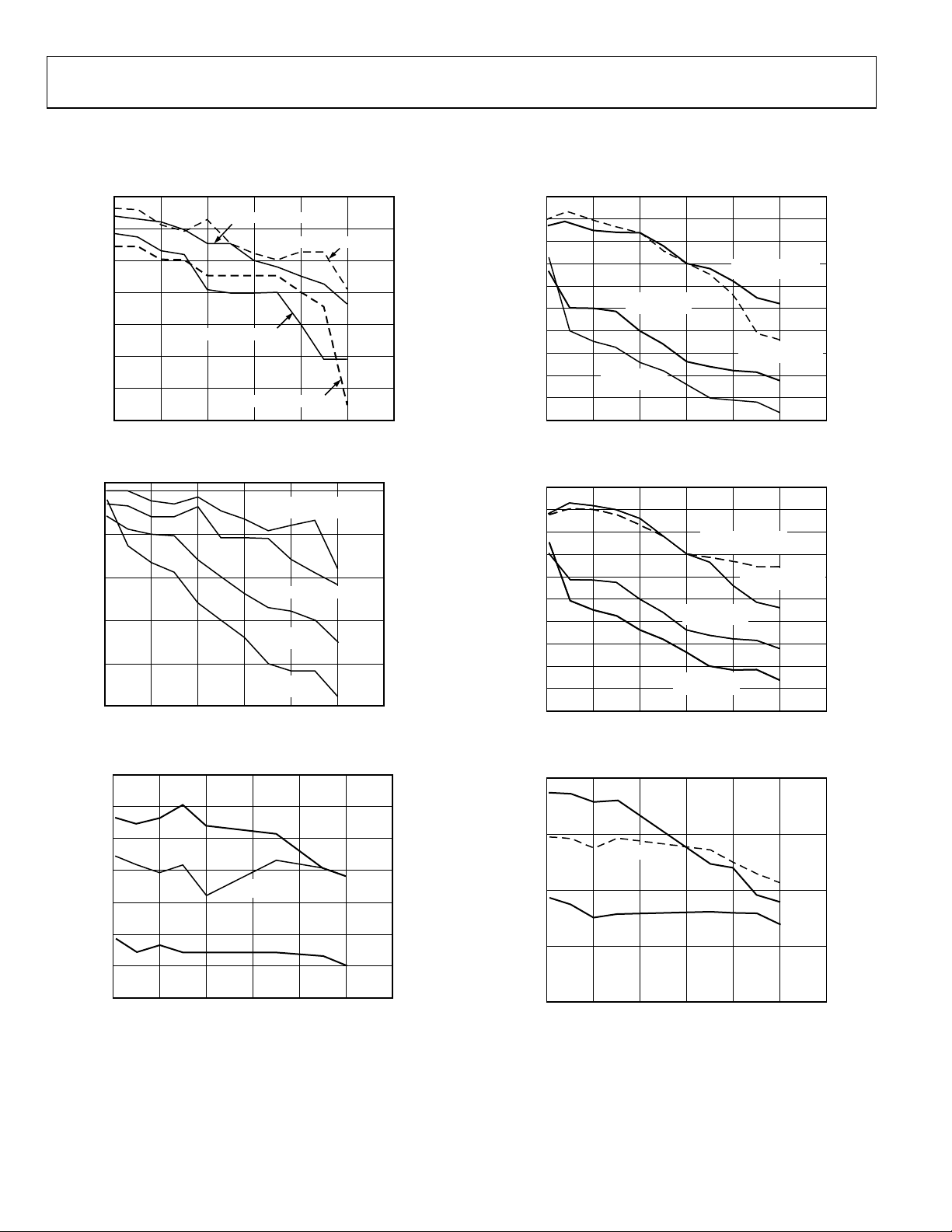
Figure 4. SNR vs. Input Frequency and Configuration
60
55
50
SINAD (dB)
45
40
35
0 20 40 60 80 100 120
INPUT FREQUENCY (MHz)
2V DIFFERENTIAL
INPUT
1V DIFFERENTIAL INPUT
1V SINGLEENDED INPUT
2V SINGLEENDED INPUT
Figure 5. SINAD vs. Input Frequency and Configuration
–75
9.6
8.8
8.0
7.1
6.3
5.5
00573-004
ENOB
00573-005
85
80
75
70
65
60
SFDR (dB)
55
50
45
40
35
0 20406080100120
1V SINGLEENDED INPUT
2V SINGLEENDED INPUT
INPUT FREQUENCY (MHz)
1V DIFFERENTIAL
INPUT
2V DIFFERENTIAL
INPUT
Figure 7. SFDR vs. Input Frequency and Configuration
–80
–75
–70
–65
–60
–55
THD (dB)
–50
–45
–40
–35
–30
0 20406080100120
INPUT FREQUENCY (MHz)
1V DIFFERENTIAL
1V DIFFERENTIAL
INPUT
INPUT
1V SINGLE-
1V SINGLEENDED INPUT
ENDED INPUT
2V SINGLE-
2V SINGLEENDED INPUT
ENDED INPUT
2V DIFFERENTIAL
INPUT
Figure 8. THD vs. Input Frequency and Configuration
–75
00573-007
00573-008
–70
–65
–60
–55
THD (dB)
–50
–45
–40
0 20406080100120
INPUT FREQUENCY (MHz)
–0.5dB
–6.0dB
–20dB
Figure 6. THD vs. Input Frequency and Amplitude
(Differential Input VREF = 0.5 V)
00573-006
Rev. B | Page 8 of 28
–0.5dB
–65
–6.0dB
–55
THD (dB)
–45
–35
0 20406080100120
INPUT FREQUENCY (MHz)
–20dB
Figure 9. THD vs. Input Frequency and Amplitude
(Differential Input VREF = 1 V )
00573-009
AD9203
1.2E+07
1.0E+07
8.0E+06
6.0E+06
HITS
4.0E+06
2.0E+06
0.0E+00
4560 10310
N–1 N N+1
10000000
CODE
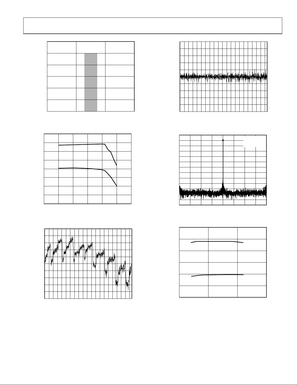
Figure 10. Grounded Input Histogram
80
85
70
65
60
55
+SNR/–THD (dB)
50
45
40
0 102030405060
SAMPLE RATE (MSPS)
Figure 11. SNR and THD vs. Sample Rate (f
1.0
0.8
0.6
0.4
0.2
0
LSB
–0.2
–0.4
–0.6
–0.8
–1.0
0 100 200 300 400 500 600 700 800 900 1024
–THD
SNR
= 20 MHz)
IN
00573-010
00573-011
00573-012
1.0
0.8
0.6
0.4
0.2
0
LSB
–0.2
–0.4
–0.6
–0.8
–1.0
0 100 200 300 400 500 600 700 800 900 1024
00573-013
Figure 13. Typical DNL Performance
10
0
–10
–20
–30
–40
–50
dB
–60
–70
–80
–90
–100
–110
–120
0E+0 2.5E+6 5.0E+6 7.5E+6 10.0E+6 12.5E+6 15.0E+6 17.5E+6 20.0E+6
SNR = 59.9dB
THD = –75dB
SFDR = 82dB
00573-014
Figure 14. Single Tone Frequency Domain Performance (Input Frequency =
10 MHz, Sample Rate = 40 MSPS 2 V Differential Input, 8192 Point FFT )
80
75
–THD
70
65
+SNR/–THD (dB)
60
55
50
2.5 3.0 3.5 4.0
SNR
SUPPLY VOLTAGE (V)
00573-015
Figure 12. Typical INL Performance
Rev. B | Page 9 of 28
Figure 15. SNR and THD vs. Power Supply
(f
= 20 MHz, Sample Rate = 40 MSPS)
IN
 Loading...