Analog Devices AD9058 d Datasheet

Dual 8-Bit 50 MSPS
a
FEATURES
2 Matched ADCs on Single Chip
50 MSPS Conversion Speed
On-Board Voltage Reference
Low Power (<1 W)
Low Input Capacitance (10 pF)
65 V Power Supplies
Flexible Input Range
APPLICATIONS
Quadrature Demodulation for Communications
Digital Oscilloscopes
Electronic Warfare
Radar
GENERAL DESCRIPTION
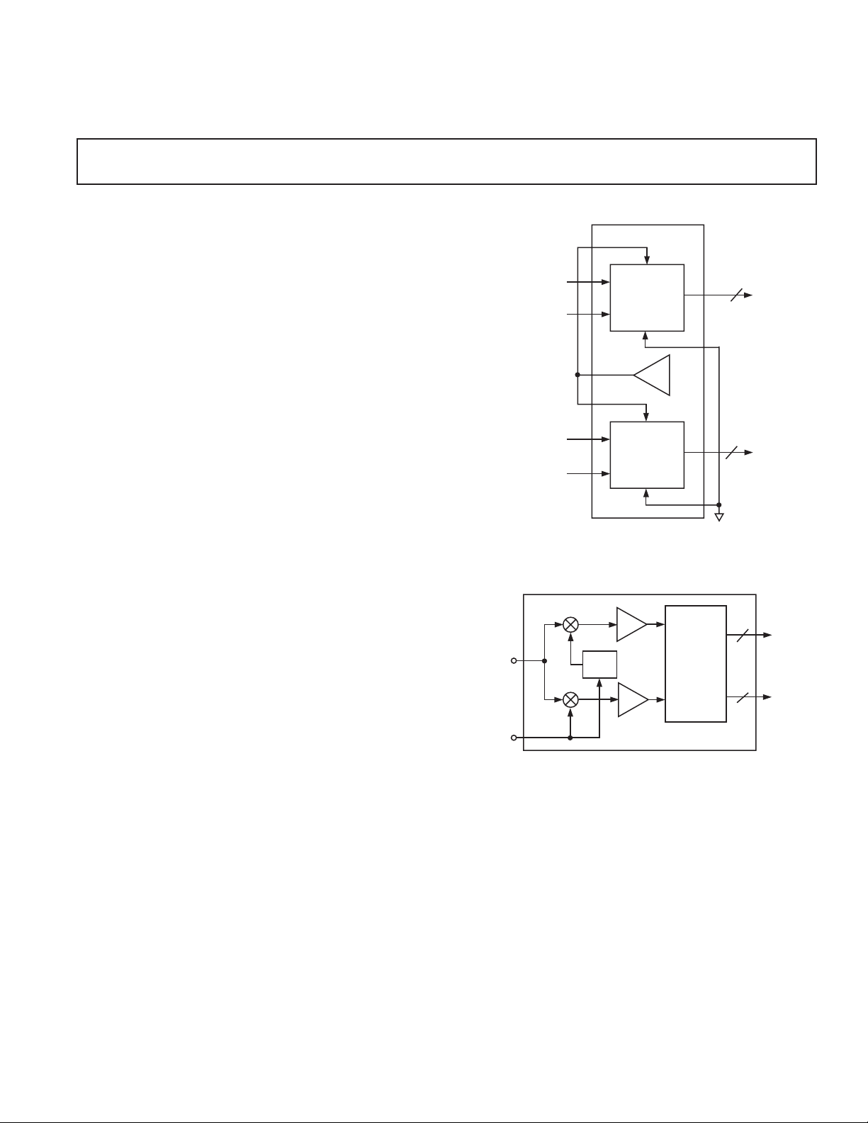
The AD9058 combines two independent, high performance,
8-bit analog-to-digital converters (ADCs) on a single monolithic
IC. Combined with an optional on-board voltage reference,
the AD9058 provides a cost-effective alternative for systems
requiring two or more ADCs.
Dynamic performance (SNR, ENOB) is optimized to provide
up to 50 MSPS conversion rates. The unique architecture
results in low input capacitance while maintaining high performance and low power (<0.5 W/channel). Digital inputs
and outputs are TTL compatible.
Performance has been optimized for an analog input of 2 V p-p
(±1 V; 0 V to 2 V). Using the on-board 2 V voltage reference,
the AD9058 can be set up for unipolar positive operation
(0 V to 2 V). This internal voltage reference can drive
both ADCs.
Commercial (0°C to 70°C) and military (–55°C to +125°C)
temperature range parts are available. Parts are supplied in
hermetic 48-lead DIP and 44-lead “J” lead packages.
A/D Converter
FUNCTIONAL BLOCK DIAGRAM
AD9058
+V
REF
RF
LO
ENCODE
A
IN
ENCODE
A
IN
QUADRATURE RECEIVER
90ⴗ
8-BIT
ANALOG-
TO-DIGITAL
CONVERTER
–V
REF
2V
8-BIT
ANALOG-
TO-DIGITAL
CONVERTER
–V
REF
G
G
REF
+V
REF
AD9058
AD9058
8
A
8
B
8
Q
8
I
REV. D
Information furnished by Analog Devices is believed to be accurate and
reliable. However, no responsibility is assumed by Analog Devices for its
use, nor for any infringements of patents or other rights of third parties that
may result from its use. No license is granted by implication or otherwise
under any patent or patent rights of Analog Devices. Trademarks and
registered trademarks are the property of their respective companies.
One Technology Way, P.O. Box 9106, Norwood, MA 02062-9106, U.S.A.
Tel: 781/329-4700 www.analog.com
Fax: 781/326-8703 © 2003 Analog Devices, Inc. All rights reserved.

AD9058–SPECIFICATIONS
ELECTRICAL CHARACTERISTICS
[ⴞVS = ⴞ5 V; V
GROUND, unless otherwise noted.]1 All specifications apply to either of the two ADCs.
= 2 V (internal); ENCODE = 40 MSPS; AIN = 0 V to 2 V; –V
REF
REF
=
Test AD9058AJD/AJJ AD9058AKD/AKJ
Parameter Temp Level Min Typ Max Min Typ Max Unit
RESOLUTION 8 8 Bits
DC ACCURACY
Differential Nonlinearity 25°CI 0.25 0.65 0.25 0.5 LSB
Full VI 0.8 0.7 LSB
Integral Nonlinearity 25°CI 0.5 1.3 0.5 1.0 LSB
Full VI 1.4 1.25 LSB
No Missing Codes Full VI Guaranteed Guaranteed
ANALOG INPUT
Input Bias Current 25°CI 75 170 75 170 µA
Full VI 340 340 µA
Input Resistance 25°CI 12 28 12 28 kΩ
Input Capacitance 25°CIV 10 15 1015 pF
Analog Bandwidth 25°CV 175 175 MHz
REFERENCE INPUT
Reference Ladder Resistance 25°CI 120 170 220 120 170 220 Ω
Full VI 80 270 80 270 Ω
Ladder Tempco Full V 0.45 0.45 Ω/°C
Reference Ladder Offset 25°CI 8 16 8 16 mV
(Top) Full VI 24 24 mV
Reference Ladder Offset 25°CI 8 23 8 23 mV
(Bottom) Full VI 33 33 mV
Offset Drift Coefficient Full V 50 50 µV/°C
INTERNAL VOLTAGE REFERENCE
Reference Voltage 25°CI 1.95 2.0 2.20 1.95 2.0 2.20 V
Full VI 1.90 2.25 1.90 2.25 V
Temperature Coefficient Full V 150 150 µV/°C
Power Supply Rejection
Ratio (PSRR) 25°CI 10 25 10 25 mV/V
SWITCHING PERFORMANCE
Maximum Conversion Rate
Aperture Delay (t
)25°CIV 0.1 0.8 1.5 0.1 0.8 1.5 ns
A
2
25°CI 50 50 60 MSPS
Aperture Delay Matching 25°CIV 0.2 0 5 0.2 0.5 ns
Aperture Uncertainty (Jitter) 25°CV 10 10 ps, rms
Output Delay (Valid) (t
Output Delay (t
) Tempco Full V 16 16 ps/°C
V
Propagation Delay (t
Propagation Delay (t
2
)
V
2
)
PD
) Tempco Full V –16 –16 ps/°C
PD
25°CI 8 5 8 ns
25°CI 12 12 19 ns
Output Time Skew 25°CV 1 1 ns
ENCODE INPUT
Logic “1” Voltage Full VI 2 2 V
Logic “0” Voltage Full VI 0.8 0.8 V
Logic “1” Current Full VI 600 600 µA
Logic “0” Current Full VI 1000 1000 µA
Input Capacitance 25°CV 5 5 pF
Pulsewidth (High) 25°CI 8 8 ns
Pulsewidth (Low) 25°CI 8 8 ns
–2–
REV. D

AD9058
Test AD9058AJD/AJJ AD9058AKD/AKJ
Parameter Temp Level Min Typ Max Min Typ Max Unit
DYNAMIC PERFORMANCE
Transient Response 25°CV 2 2 ns
Overvoltage Recovery Time 25°CV 2 2 ns
Effective Number of Bits (ENOB)
Analog Input @ 2.3 MHz 25°CI 7.7 7.2 7.7 Bits
@ 10.3 MHz 25°CI 7.4 7.1 7.4 Bits
Signal-to-Noise Ratio
3
Analog Input @ 2.3 MHz 25°CI 48 45 48 dB
@ 10.3 MHz 25°CI 46 44 46 dB
3
Signal-to-Noise Ratio
(Without Harmonics)
Analog Input @ 2.3 MHz 25°CI 48 46 48 dB
@ 10.3 MHz 25°CI 47 45 47 dB
Second Harmonic Distortion
Analog Input @ 2.3 MHz 25°CI 58 48 58 dBc
@ 10.3 MHz 25°CI 58 48 58 dBc
Third Harmonic Distortion
Analog Input @ 2.3 MHz 25°CI 58 50 58 dBc
@ 10.3 MHz 25°CI 58 50 58 dBc
Crosstalk Rejection
4
DIGITAL OUTPUTS
Logic “1” Voltage (I
= 2 mA) Full VI 2.4 2.4 V
OH
Logic “0” Voltage (IOL = 2 mA) Full VI 0.4 0.4 V
POWER SUPPLY
5
+VS Supply Current Full VI 127 154 127 154 mA
Supply Current Full VI 27 38 27 38 mA
–V
S
Power Dissipation Full VI 770 960 770 960 mW
NOTES
1
For applications in which +VS may be applied before –VS, or +VS current is not limited to 500 mA, a reverse-biased clamping diode should be inserted between
ground and –VS to prevent destructive latch up. See section entitled “Using the AD9058.”
2
To achieve guaranteed conversion rate, connect each data output to ground through a 2 k Ω pull-down resistor.
3
SNR performance limits for the 48-lead DIP “D” package are 1 dB less than shown. ENOB limits are degraded by 0.3 dB. SNR and ENOB measured with
analog input signal 1 dB below full scale at specified frequency.
4
Crosstalk rejection measured with full-scale signals of different frequencies (2.3 MHz and 3.5 MHz) applied to each channel. With both signals synchronously
encoded at 40 MSPS, isolation of the undesired frequency is measured with an FFT.
5
Applies to both A/Ss and includes internal ladder dissipation.
Specifications subject to change without notice.
3
25°CIV 60 4860 dBc
REV. D
–3–

AD9058
ABSOLUTE MAXIMUM RATINGS
1
Analog Input . . . . . . . . . . . . . . . . . . . . . . . . –1.5 V to +2.5 V
. . . . . . . . . . . . . . . . . . . . . . . . . . . . . . . . . . . . . . . . . . 6 V
+V
S
–VS . . . . . . . . . . . . . . . . . . . . . . . . . . . . . . . . +0.8 V to –6 V
Digital Inputs . . . . . . . . . . . . . . . . . . . . . . . . . –0.5 V to +V
2
S
Digital Output Current . . . . . . . . . . . . . . . . . . . . . . . . 20 mA
Voltage Reference Current . . . . . . . . . . . . . . . . . . . . . . 53 mA
+V
–V
. . . . . . . . . . . . . . . . . . . . . . . . . . . . . . . . . . . . . . 2.5 V
REF
. . . . . . . . . . . . . . . . . . . . . . . . . . . . . . . . . . . . . –1.5 V
REF
Operating Temperature Range
AD9058AJD/AJJ/AKD/AKJ . . . . . . . . . . . . . . . 0°C to 70°C
Maximum Junction Temperature
3
AD9058AJD/AJJ/AKD/AKJ . . . . . . . . . . . . . . . . . . . 150°C
Storage Temperature Range . . . . . . . . . . . . –65°C to +150°C
Lead Temperature (Soldering, 10 sec) . . . . . . . . . . . . . 300°C
NOTES
1
Absolute maximum ratings are limiting values to be applied individually, and
beyond which the serviceability of the circuit may be impaired. Functional
operability is not necessarily implied. Exposure to absolute maximum rating
conditions for an extended period of time may affect device reliability.
2
For applications in which +VS may be applied before –VS, or +VS current is
not limited to 500 mA, a reverse-biased clamping diode should be inserted
between ground and –VS to prevent destructive latch up. See section entitled
“Using the AD9058.”
3
Typical thermal impedances: 44-lead hermetic J-leaded ceramic package: θJA = 86.4°C/W;
θJC = 24.9°C/W; 48-lead hermetic: DIP θJA = 40°C/W; θ
= 12°C/W.
JC
EXPLANATION OF TEST LEVELS
Test Level
I. 100% production tested.
II. 100% production tested at 25°C, and sample tested at
specified temperatures.
III. Sample tested only.
IV. Parameter is guaranteed by design and characterization
testing.
V. Parameter is a typical value only.
VI. All devices are 100% production tested at 25°C. 100%
production tested at temperature extremes for extended
temperature devices; sample tested at temperature
extremes for commercial/industrial devices.
ORDERING GUIDE
Temperature Package
Model Range Description Option
AD9058AJJ 0°C to 70°C 44-Lead J-Leaded J-44
AD9058AJJ-REEL 0°C to 70°C 44-Lead J-Leaded J-44
Ceramic
Ceramic
2
2
AD9058AKJ 0°C to 70°C 44-Lead J-Leaded J-44
Ceramic, AC Tested
AD9058ATJ/883
3
–55°C to +125°C 44-Lead J-Leaded J-44
Ceramic, AC Tested
AD9058AJD 0°C to 70°C 48-Lead Ceramic DIP D-48
AD9058AKD 0°C to 70°C 48-Lead Ceramic D-48
AD9058ATD/883
3
–55°C to +125°C 48-Lead Ceramic D-48
DIP, AC Tested
DIP, AC Tested
NOTES
1
D = Hermetic ceramic DIP package; J = leaded ceramic package.
2
Hermetically sealed ceramic package; footprint equivalent to PLCC.
3
For specifications, refer to Analog Devices Military Products Databook.
1
CAUTION
ESD (electrostatic discharge) sensitive device. Electrostatic charges as high as 4000 V readily
accumulate on the human body and test equipment and can discharge without detection. Although
the AD9058 features proprietary ESD protection circuitry, permanent damage may occur on
devices subjected to high energy electrostatic discharges. Therefore, proper ESD precautions are
recommended to avoid performance degradation or loss of functionality.
+V
S
5V
S
13k⍀
DIGITAL BITS
Equivalent Digital Outputs
ENCODE
Equivalent Encode Circuit
0.1F
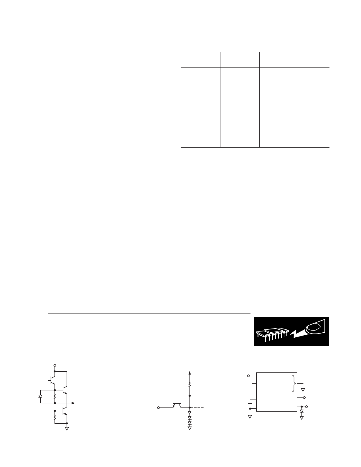
* INDICATES EACH PIN IS CONNECTED THROUGH 2k⍀
** INDICATES EACH PIN IS CONNECTED THROUGH 100⍀
–4–
WARNING!
ESD SENSITIVE DEVICE
D0–D7*+V
+V
INT
+V
REF
COMP
GROUND
Burn-In Connections
ENCODE**
AD9058
–V
REF
**
A
IN
+V
S
–V
S
+5V
–5.2V
REV. D
 Loading...