Analog Devices AD876 Datasheet

10-Bit 20 MSPS 160 mW
A/D
D/A
A/D
D/A A/D D/A
A/D
CORRECTION LOGIC
AIN
REFTF
REFTS
REFBS
REFBF
STBY
THREE-
STATE
(MSB)
D9
D0
(LSB)
DRV
DD
DV
DD
AV
DD
CLK
DRV
SS
DV
SS
AV
SS
CML
AD876
SHA SHA SHAGAIN SHA GAINGAIN
OUTPUT BUFFERS
a
FEATURES
CMOS 10-Bit 20 MSPS Sampling A/D Converter
Pin-Compatible 8-Bit Option
Power Dissipation: 160 mW
+5 V Single Supply Operation
Differential Nonlinearity: 0.5 LSB
Guaranteed No Missing Codes
Power Down (Standby) Mode
Three-State Outputs
Digital I/Os Compatible with +5 V or +3.3 V Logic
Adjustable Reference Input
Small Size: 28-Lead SOIC, 28-Lead SSOP, or 48-Lead
Thin Quad Flatpack (TQFP)
PRODUCT DESCRIPTION
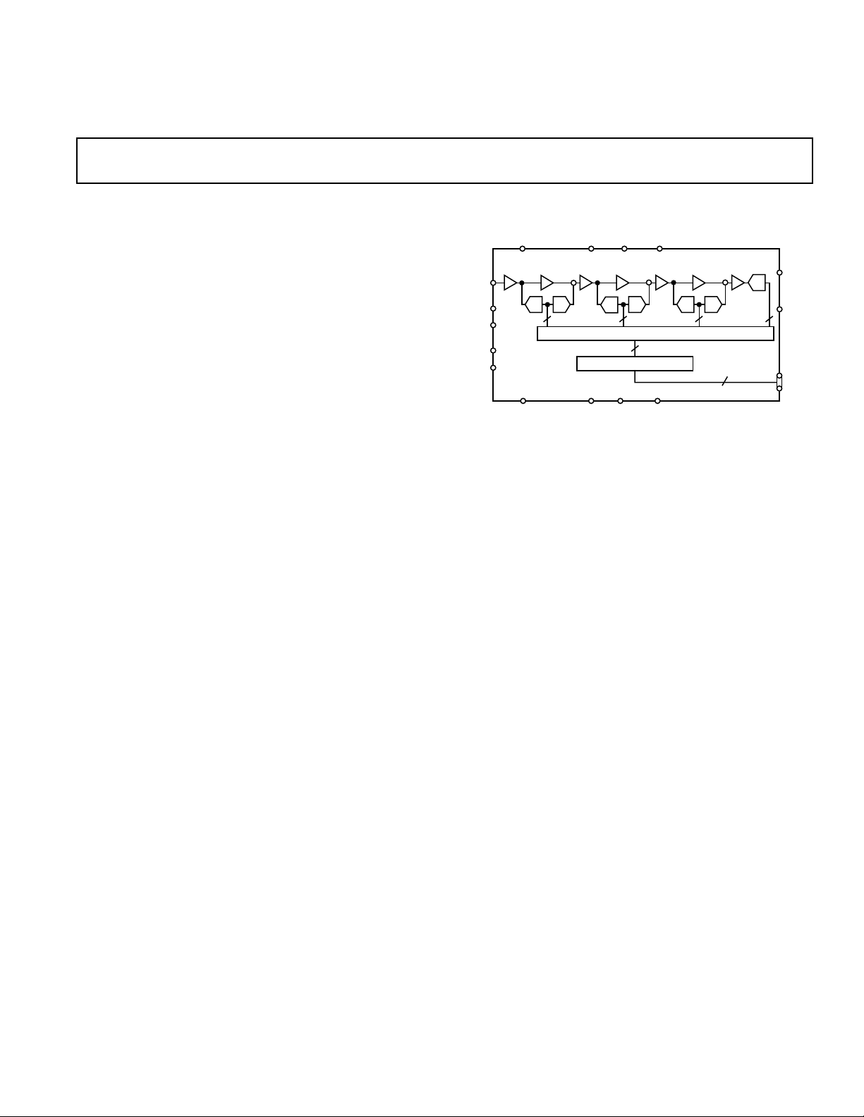
The AD876 is a CMOS, 160 mW, 10-bit, 20 MSPS analog-todigital converter (ADC). The AD876 has an on-chip input
sample-and-hold amplifier. By implementing a multistage pipelined architecture with output error correction logic, the AD876
offers accurate performance and guarantees no missing codes
over the full operating temperature range. Force and sense connections to the reference inputs minimize external voltage drops.
The AD876 can be placed into a standby mode of operation
reducing the power below 50 mW. The AD876’s digital I/O
interfaces to either +5 V or +3.3 V logic. Digital output pins
can be placed in a high impedance state; the format of the output is straight binary coding.
The AD876’s speed, resolution and single-supply operation
ideally suit a variety of applications in video, multimedia, imaging, high speed data acquisition and communications. The
AD876’s low power and single-supply operation satisfy requirements for high speed portable applications. Its speed and resolution ideally suit charge coupled device (CCD) input systems
such as color scanners, digital copiers, electronic still cameras
and camcorders.
CMOS A/D Converter
AD876
FUNCTIONAL BLOCK DIAGRAM
The AD876 comes in a space saving 28-lead SOIC and 48-lead
thin quad flatpack (TQFP) and is specified over the commercial
(0°C to +70°C) temperature range.
PRODUCT HIGHLIGHTS
Low Power
The AD876 at 160 mW consumes a fraction of the power of
presently available 8- or 10-bit, video speed converters. Powerdown mode and single-supply operation further enhance its
desirability in low power, battery operated applications such
as electronic still cameras, camcorders and communication
systems.
Very Small Package
The AD876 comes in a 28-lead SOIC, 28-lead SSOP, and 48lead surface mount, thin quad flat package. The TQFP package
is ideal for very tight, low headroom designs.
Digital I/O Functionality
The AD876 offers three-state output control.
Pin Compatible Upgrade Path
The AD876 offers the option of laying out designs for eight
bits and migrating to 10-bit resolution if prototype results
warrant.
REV. B
Information furnished by Analog Devices is believed to be accurate and
reliable. However, no responsibility is assumed by Analog Devices for its
use, nor for any infringements of patents or other rights of third parties
which may result from its use. No license is granted by implication or
otherwise under any patent or patent rights of Analog Devices.
One Technology Way, P.O. Box 9106, Norwood, MA 02062-9106, U.S.A.
Tel: 781/329-4700 World Wide Web Site: http://www.analog.com
Fax: 781/326-8703 © Analog Devices, Inc., 1998

(T
to T
AD876–SPECIFICATIONS
MIN
+2.0 V, f
with AVDD = +5.0 V, DVDD = +5.0 V, DRVDD = +3.3 V, V
MAX
= 20 MSPS, unless otherwise noted)
CLOCK
= +4.0 V, V
REFB
REFB
=
AD876JR-8 AD876
Parameter Min Typ Max Min Typ Max Units
RESOLUTION 8 10 Bits
DC ACCURACY
Integral Nonlinearity (INL) ±0.3 ±1.0 ±1.0 LSB
Differential Nonlinearity (DNL) ±0.1 ±0.75 ±0.5 ±1 LSB
No Missing Codes GUARANTEED GUARANTEED
Offset Error 0.1 0.4 % FSR
Gain Error 0.1 0.2 % FSR
ANALOG INPUT
Input Range 2 2 V p-p
Input Capacitance 5.0 5.0 pF
REFERENCE INPUT
Reference Top Voltage 3.5 4.0 4.5 3.5 4.0 4.5 V
Reference Bottom Voltage 1.6 2.0 2.5 1.6 2.0 2.5 V
Reference Input Resistance 250 250 Ω
Reference Input Current 8.0 8.0 mA
Reference Top Offset 35 35 mV
Reference Bottom Offset 35 35 mV
DYNAMIC PERFORMANCE
Effective Number of Bits
fIN = 1 MHz 7.8 9.0 Bits
= 3.58 MHz 7.4 7.8 8.2 9.0 Bits
f
IN
= 10 MHz 7.5 8.2 Bits
f
IN
Signal-to-Noise and Distortion (S/N+D) Ratio
= 1 MHz 49 56 dB
f
IN
= 3.58 MHz 46 49 51 56 dB
f
IN
= 10 MHz 47 51 dB
f
IN
Total Harmonic Distortion (THD)
=1 MHz –62 –62 dB
f
IN
= 3.58 MHz –62 –56 –62 –56 dB
f
IN
=10 MHz –60 –60 dB
f
IN
Spurious Free Dynamic Range
2
–65 –65 dB
Full Power Bandwidth 150 150 MHz
Differential Phase 0.5 0.5 Degree
Differential Gain 1 1 %
POWER SUPPLIES
Operating Voltage
AV
DD
DV
DRV
DD
DD
1
1
+4.5 +5.25 +4.5 +5.25 Volts
+4.5 +5.25 +4.5 +5.25 Volts
+3.0 +5.25 +3.0 +5.25 Volts
Operating Current
IAV
DD
IDV
DD
IDRV
DD
20 25 20 25 mA
12 16 12 16 mA
0.1 1 0.1 1 mA
POWER CONSUMPTION 160 190 160 190 mW
TEMPERATURE RANGE
Specified 0 +70 0 +70 °C
NOTES
1
AVDD and DVDD must be within 0.5 V of each other to maintain specified performance levels.
2
3.58 MHz Input Frequency.
Specifications subject to change without notice. See Definition of Specifications for additional information.
REV. B–2–

(T
to T
DIGITAL SPECIFICATIONS
with AVDD = +5.0 V, DVDD = +5.0 V, DRVDD = +3.3 V, V
MAX
= 20 MSPS, CL = 20 pF unless otherwise noted)
f
CLOCK
MIN
= +4.0 V, V
REFT
AD876
Parameter Symbol DRV
Min Typ Max Units
DD
LOGIC INPUT
High Level Input Voltage V
IH
3.0 2.4 V
5.0 4.0 V
5.25 4.2 V
Low Level Input Voltage V
IL
3.0 0.6 V
5.0 1.0 V
5.25 1.05 V
High Level Input Current I
Low Level Input Current I
Low Level Input Current (CLK Only) I
Input Capacitance C
IH
IL
IL
IN
5.0 –10 +10 µA
5.0 –50 +50 µA
5.0 –10 +10 µA
5pF
LOGIC OUTPUTS
High Level Output Voltage V
OH
(IOH = 50 µA) 3.0 2.4 V
5.0 3.8 V
= 0.5 mA) 5.0 2.4 V
(I
OH
Low Level Output Voltage V
OL
(IOL = 50 µA) 3.6 0.7 V
5.25 1.05 V
= 0.6 mA) 5.25 0.4 V
(I
OL
Output Capacitance C
Output Leakage Current I
Specifications subject to change without notice.
OUT
OZ
–10 10 µA
5pF
AD876
= +2.0 V,
REFB
TIMING SPECIFICATIONS
Symbol Min Typ Max Units
Maximum Conversion Rate
Clock Period t
Clock High t
Clock Low t
Output Delay t
Pipeline Delay (Latency) 3.5 Clock Cycles
Aperture Delay Time 4 ns
Aperture Jitter 22 ps
NOTE
1
Conversion rate is operational down to 10 kHz without degradation in specified performance.
1
C
CH
CL
OD
SAMPLE N SAMPLE N+1 SAMPLE N+2
AIN
t
t
CL
CH
CLK
t
C
OUT DATA N-4 DATA N-3 DATA N-2 DATA N-1 DATA N
20 MHz
50 ns
23 25 ns
23 25 ns
10 20 ns
t
OD
REV. B
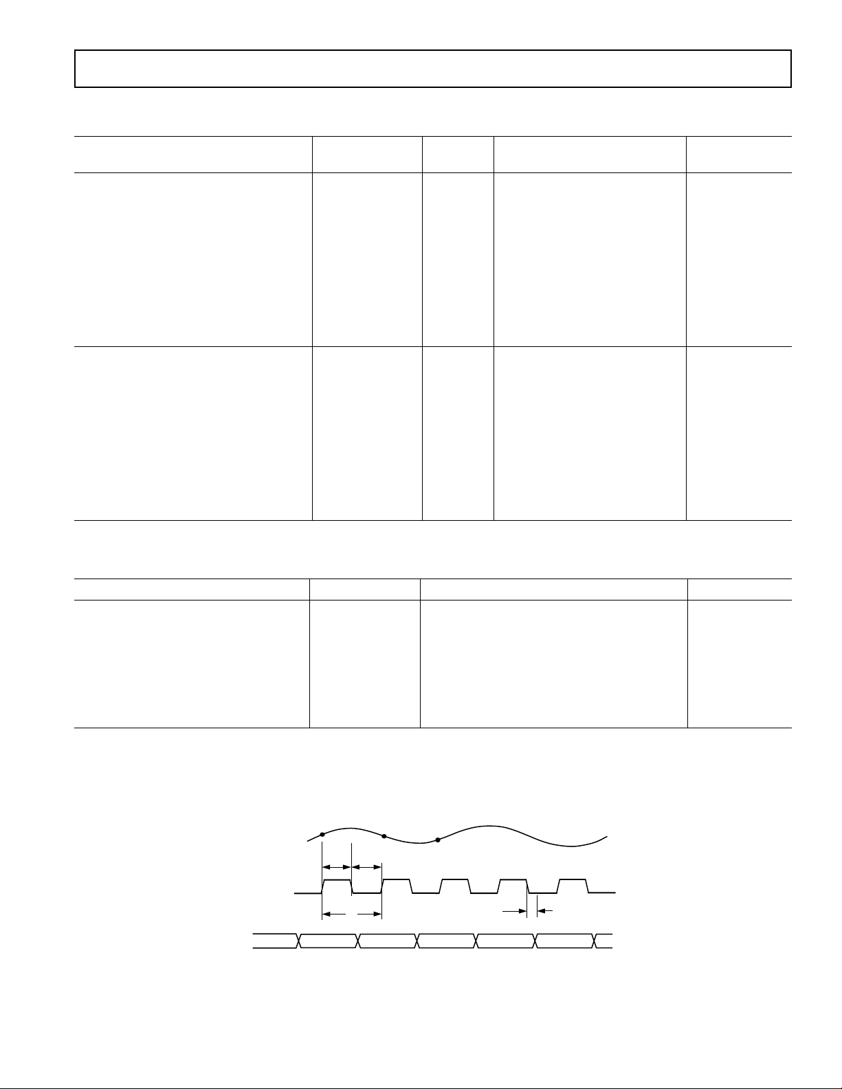
Figure 1. Timing Diagram
–3–

AD876
REFBS
REFTF
REFBF
D0
D1
D4
D5
D6
D2
D3
DV
SS
DV
DD
REFTS
D8
D9
D7
41
424347 4546
17 20191814 1615
36
35
32
31
30
34
33
44
1
2
5
6
7
3
4
373839
21 242322
40
28
27
26
29
9
10
11
8
48
13
25
12
TOP VIEW
(Not to Scale)
AD876
DRV
SSDVSS
CLK
THREE-STATE
STBY
DRV
DD
AVSSAV
DD
AIN
CML
DV
SS
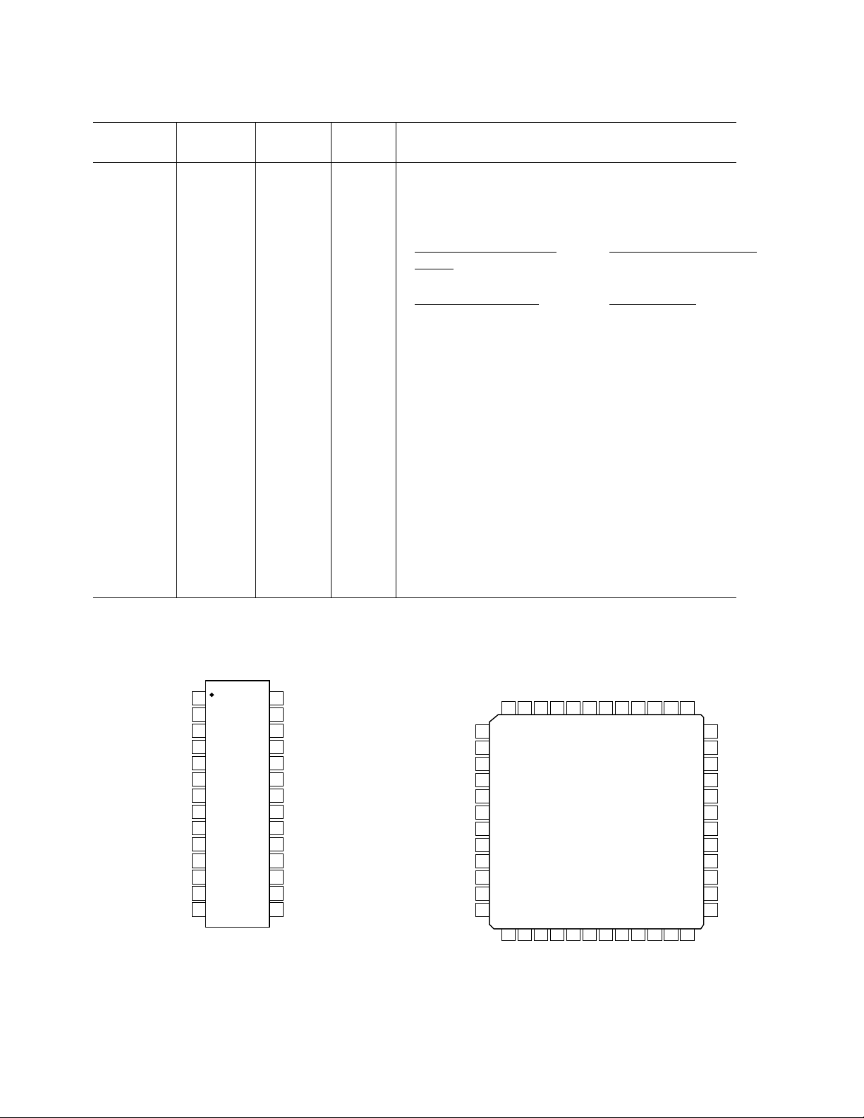
PIN FUNCTION DESCRIPTIONS
SOIC TQFP
Symbol Pin No. Pin No. Type Name and Function
D0 (LSB) 3 1 DO Least Significant Bit.
D1–D4 4–7 2–5 DO Data Bits 1 through 4.
D5–D8 8–11 8–11 Data Bits 5 through 8.
D9 (MSB) 12 12 DO Most Significant Bit.
THREE- 16 23 DI
STATE
STBY 17 24 DI
CLK 15 22 DI Clock Input.
CML 26 38 AO Bypass Pin for an Internal Bias Point.
REFTF 22 30 AI Reference Top Force.
REFBF 24 34 AI Reference Bottom Force.
REFTS 21 29 AI Reference Top Sense.
REFBS 25 35 AI Reference Bottom Sense.
AIN 27 39 AI Analog Input.
AV
DD
AV
SS
DV
DD
DV
SS
DRV
DD
DRV
SS
Type: AI = Analog Input; AO = Analog Output; DI = Digital Input; DO = Digital Output; P = Power.
28 42 P +5 V Analog Supply.
1 44 P Analog Ground.
18 26 P +5 V Digital Supply.
14, 19, 20 17, 27, 28 P Digital Ground.
2 45 P +3.3 V/+5 V Digital Supply. Supply for digital
13 16 P +3.3 V/+5 V Digital Ground. Ground for digital
THREE-STATE = LOW THREE-STATE = HIGH
or N/C
Normal Operating Mode High Impedance Outputs
STBY = LOW or N/C STBY = HIGH
Normal Operating Mode Standby Mode
input and output buffers.
input and output buffers.
PIN CONFIGURATIONS
SOIC/SSOP TQFP
AV
1
SS
DRV
2
DD
3
*D0
4
*D1
5
D2
D3
6
D4
D5 REFTS
D6
D7
D8
D9 STBY
DRV
SS
DV
SS
*
PINS D0 AND D1 ARE LEFT OPEN
FOR THE AD876JR-8
AD876
7
TOP VIEW
8
(Not to Scale)
9
10
11
12
13
14
NC = NO CONNECT
28
AV
DD
AIN
27
26
CML
25
REFBS
REFBF
24
23
NC
REFTF
22
21
20
DV
SS
DV
19
SS
18
DV
DD
17
THREE-STATE
16
CLK
15
REV. B–4–

AD876
WARNING!
ESD SENSITIVE DEVICE
ABSOLUTE MAXIMUM RATINGS*
Parameter With Respect to Min Max Units
AV
DV
AV
DD
DD
SS
, DRV
DD
AV
DVSS, DRV
DVSS, DRV
AIN AV
SS
SS
–0.5 +6.5 Volts
–0.5 +6.5 Volts
SS
–0.5 +0.5 Volts
SS
–0.5 +6.5 Volts
REFTS, REFTF
REFBS, REFBF AV
Digital Inputs, CLK DV
SS
, DRV
SS
–0.5 +6.5 Volts
–0.5 +6.5 Volts
SS
Junction Temperature +150 °C
Storage Temperature –65 +150 °C
Lead Temperature
(10 sec) +300 °C
*Stresses above those listed under Absolute Maximum Ratings may cause perma-
nent damage to the device. This is a stress rating only; functional operation of the
device at these or any other conditions above those indicated in the operational
sections of this specification is not implied. Exposure to absolute maximum
ratings for extended periods may effect device reliability.
DV
DD
DRV
DV
DD
DV
SS
DRV
SS
SS
DV
DV
DD
SS
a) D0–D9 b) Three-State, Standby
ORDERING GUIDE
Temperature Package Package
Model Range Description Options
AD876JR 0°C to +70°C 28-Lead SOIC R-28
AD876JST-Reel 0°C to +70°C 48-Lead TQFP ST-48
(Tape and Reel 13")
AD876JR-8 0°C to +70°C 28-Lead SOIC R-28
AD876AR –40°C to +85°C 28-Lead SOIC R-28
AD876ARS –40°C to +85°C 28-Lead SSOP RS-28
AD876JRS 0°C to +70°C 28-Lead SSOP RS-28
AD876JRS-8 0°C to +70°C 28-Lead SSOP RS-28
DRV
DRV
DV
DD
DD
DV
SS
SS
DRV
DRV
DD
SS
c) CLK
AV
DD
REFTF
AV
AV
DD
AV
SS
d) AIN
AV
REFTS
AV
REFBS
AV
REFBF
SS
DD
INTERNAL
REFERENCE
AV
SS
DD
AV
SS
DD
AV
SS
VOLTAGE
INTERNAL
REFERENCE
VOLTAGE
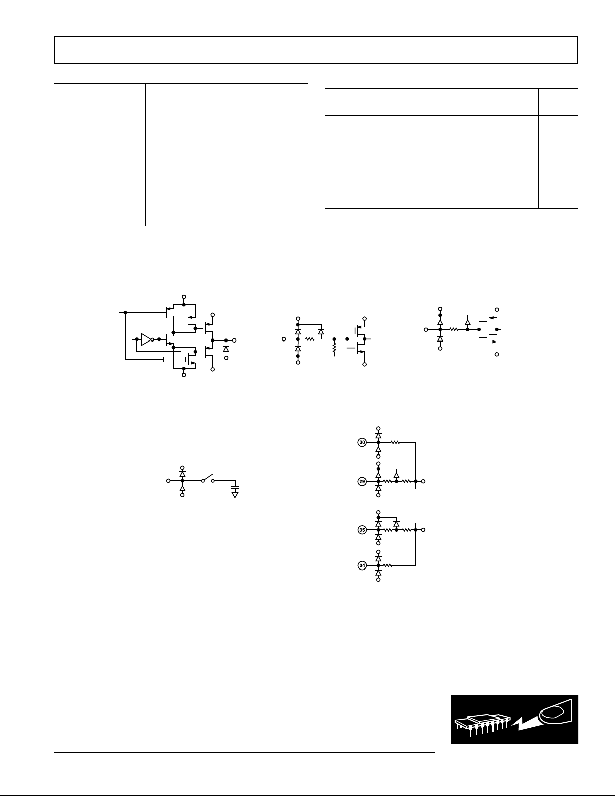
Figure 2. Equivalent Circuits
CAUTION
ESD (electrostatic discharge) sensitive device. Electrostatic charges as high as 4000 V readily
accumulate on the human body and test equipment and can discharge without detection.
Although the AD876 features proprietary ESD protection circuitry, permanent damage may
occur on devices subjected to high energy electrostatic discharges. Therefore, proper ESD
precautions are recommended to avoid performance degradation or loss of functionality.
REV. B
–5–
 Loading...