Analog Devices AD872A Datasheet

Complete 12-Bit 10 MSPS
4 4 3 4
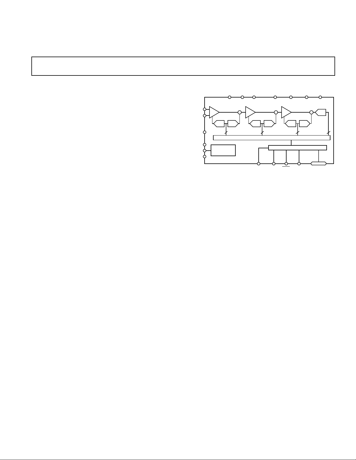
CORRECTION LOGIC
+2.5V
REFERENCE
OUTPUT BUFFERS
*OEN
OTR
*MSB BIT2–BIT12
REF GND
MSB
AV
DD
AGND
DGND
AV
SS
DV
DD
V
INA
V
INB
CLOCK
REF IN
*ONLY AVAILABLE ON 44-TERMINAL SURFACE MOUNT PACKAGE
AD872A
T/H
DAC
A/D
A/DT/H
DAC
A/D
T/H
A/D
DAC
*DRV
DD
*DRGND
REF OUT
+ + +
a
FEATURES
Monolithic 12-Bit 10 MSPS A/D Converter
Low Noise: 0.26 LSB RMS Referred-to-Input
No Missing Codes Guaranteed
Differential Nonlinearity Error: 0.5 LSB
Signal-to-Noise and Distortion Ratio: 68 dB
Spurious-Free Dynamic Range: 75 dB
Power Dissipation: 1.03 W
Complete: On-Chip Track-and-Hold Amplifier and
Voltage Reference
Twos Complement Binary Output Data
Out-of-Range Indicator
28-Lead Ceramic DIP or 44-Terminal Leadless Chip
Carrier Package
PRODUCT DESCRIPTION
The AD872A is a monolithic 12-bit, 10 MSPS analog-to-digital
converter with an on-chip, high performance track-and-hold
amplifier and voltage reference. The AD872A uses a multistage
differential pipelined architecture with error correction logic to
provide 12-bit accuracy at 10 MSPS data rates and guarantees
no missing codes over the full operating temperature range. The
AD872A is a redesigned version of the AD872 which has been
optimized for lower noise. The AD872A is pin compatible with
the AD872, allowing the parts to be used interchangeably as system requirements change.
The low noise input track-and-hold (T/H) of the AD872A is
ideally suited for high-end imaging applications. In addition, the
T/H’s high input impedance and fast settling characteristics allow the AD872A to easily interface with multiplexed systems
that switch multiple signals through a single A/D converter. The
dynamic performance of the T/H also renders the AD872A suitable for sampling single channel inputs at frequencies up to and
beyond the Nyquist rate. The AD872A provides both reference
output and reference input pins, allowing the onboard reference
to serve as a system reference. An external reference can also be
chosen to suit the dc accuracy and temperature drift requirements of the application. A single clock input is used to control
all internal conversion cycles. The digital output data is presented in twos complement binary output format. An out-ofrange signal indicates an overflow condition, and can be used
with the most significant bit to determine low or high overflow.
Monolithic A/D Converter
AD872A
FUNCTIONAL BLOCK DIAGRAM
The AD872A is fabricated on Analog Devices’ ABCMOS-l
process that utilizes high speed bipolar and CMOS transistors
on a single chip.
The AD872A is packaged in a 28-lead ceramic DIP and a 44terminal leadless ceramic surface mount package (LCC). Operation is specified from 0°C to +70°C and –55°C to +125°C.
PRODUCT HIGHLIGHTS
The AD872A offers a complete single-chip sampling, 12-bit
10 MSPS analog-to-digital conversion function in a 28-lead DIP
or 44-terminal LCC.
Low Noise—The AD872A features 0.26 LSB rms referred toinput noise.
Low Power—The AD872A at 1.03 W consumes a fraction of the
power of presently available hybrids.
On-Chip Track-and-Hold (T/H)—The low noise, high impedance T/H input eliminates the need for external buffers and can
be configured for single-ended or differential inputs.
Ease of Use—The AD872A is complete with T/H and voltage
reference and is pin-compatible with the AD872.
Out of Range (OTR)—The OTR output bit indicates when the
input signal is beyond the AD872A’s input range.
REV. A
Information furnished by Analog Devices is believed to be accurate and
reliable. However, no responsibility is assumed by Analog Devices for its
use, nor for any infringements of patents or other rights of third parties
which may result from its use. No license is granted by implication or
otherwise under any patent or patent rights of Analog Devices.
One Technology Way , P.O. Box 9106, Norwood, MA 02062-9106, U.S.A.
Tel: 781/329-4700 World Wide Web Site: http://www.analog.com
Fax: 781/326-8703 © Analog Devices, Inc., 1997

AD872A–SPECIFICA TIONS
(T
to T
DC SPECIFICATIONS
MIN
Parameter J Grade
, AVDD = + 5 V, DVDD = +5 V, AVSS = –5 V, f
MAX
1
RESOLUTION 12 12 Bits min
MAX CONVERSION RATE 10 10 MHz min
INPUT REFERRED NOISE 0.26 0.26 LSB rms typ
ACCURACY
Integral Nonlinearity (INL) ± 1.75 ±1.75 LSB typ
Differential Nonlinearity (DNL) ±0.5 ±0.5 LSB typ
No Missing Codes 12 12 Bits Guaranteed
Zero Error (@ +25°C)
Gain Error (@ +25°C)
2
2
±0.75 ±0.75 % FSR max
±1.25 ±1.25 % FSR max
TEMPERATURE DRIFT
Zero Error ±0.15 ±0.3 % FSR max
Gain Error
Gain Error
POWER SUPPLY REJECTION
3, 4
3, 5
±0.80 ±1.75 % FSR max
±0.25 ±0.50 % FSR max
6
AVDD, DVDD (+5 V ± 0.25 V) ±0.125 ±0.125 % FSR max
AVSS (–5 V ± 0.25 V) ±0.125 ±0.125 % FSR max
ANALOG INPUT
Input Range ±1.0 ±1.0 V max
Input Resistance 50 50 kΩ typ
Input Capacitance 10 10 pF typ
= 10 MHz unless otherwise noted)
SAMPLE
S Grade
1
Units
INTERNAL VOLTAGE REFERENCE
Output Voltage 2.5 2.5 V typ
Output Voltage Tolerance ±20 ±40 mV max
Output Current (Available for External Loads) 2.0 2.0 mA typ
(External Load Should Not Change During Conversion)
REFERENCE INPUT RESISTANCE 5 5 kΩ
POWER SUPPLIES
Supply Voltages
AV
DD
AV
SS
DV
DRV
DD
DD
7
+5 +5 V (±5% AVDD Operating)
–5 –5 V (±5% AVSS Operating)
+5 +5 V (±5% DVDD Operating)
+5 +5 V (±5% DRVDD Operating)
Supply Current
IAV
DD
IAV
SS
IDV
DD
IDRV
DD
7
91 92 mA max (85 mA typ)
147 150 mA max (115 mA typ)
20 21 mA max (7 mA typ)
22mA
POWER CONSUMPTION 1.03 1.03 W typ
1.25 1.3 W max
NOTES
1
Temperature ranges are as follows: J Grade: 0°C to +70° C, S Grade: –55° C to +125 ° C.
2
Adjustable to zero with external potentiometers (see Zero and Gain Error Calibration section).
3
+25°C to T
4
Includes internal voltage reference drift.
5
Excludes internal voltage reference drift.
6
Change in Gain Error as a function of the dc supply voltage (V
7
LCC package only.
Specifications subject to change without notice.
and +25°C to T
MIN
MAX
.
to V
NOMINAL
MIN
, V
NOMINAL
to V
MAX
).
–2–
REV. A

AD872A
AC SPECIFICATIONS
MIN
, AVDD = + 5 V, DVDD = +5 V, AVSS = –5 V, f
MAX
= 10 MHz unless otherwise noted)
SAMPLE
(T
to T
Parameter J Grade S Grade Units
SIGNAL-TO-NOISE & DISTORTION RATIO (S/N+D)
= l MHz 68 68 dB typ
f
INPUT
61 61 dB min
f
= 4.99 MHz 66 66 dB typ
INPUT
SIGNAL-TO-NOISE RATIO (SNR)
f
= 1 MHz 69 69 dB typ
INPUT
f
= 4.99 MHz 67 67 dB typ
INPUT
TOTAL HARMONIC DISTORTION (THD)
= 1 MHz –74 –74 dB typ
f
INPUT
–63 –62 dB max
f
= 4.99 MHz –72 –72 dB typ
INPUT
SPURIOUS-FREE DYNAMIC RANGE (SFDR)
= l MHz 75 75 dB typ
f
INPUT
f
= 4.99 MHz 74 74 dB typ
INPUT
INTERMODULATION DISTORTION (IMD)
2
Second Order Products –80 –80 dB typ
Third Order Products –73 –73 dB typ
FULL POWER BANDWIDTH 35 35 MHz typ
1
SMALL SIGNAL BANDWIDTH 35 35 MHz typ
APERTURE DELAY 6 6 ns typ
APERTURE JITTER 16 16 ps rms typ
ACQUISITION TO FULL-SCALE STEP 40 40 ns typ
OVERVOLTAGE RECOVERY TIME 40 40 ns typ
NOTES
1
f
amplitude = –0.5 dB full scale unless otherwise indicated. All measurements referred to a 0 dB (1.0 V pk) input signal unless otherwise indicated.
INPUT
2
fa = 1.0 MHz, fb = 0.95 MHz with t
Specifications subject to change without notice.
DIGITAL SPECIFICATIONS
SAMPLE
= 10 MHz.
(T
MIN
to T
, AVDD = + 5 V, DVDD = +5 V, AVSS = –5 V, f
MAX
= 10 MHz unless otherwise noted)
SAMPLE
Parameter Symbol J, S Grades Units
LOGIC INPUTS
High Level Input Voltage V
Low Level Input Voltage V
High Level Input Current (V
Low Level Input Current (V
= DVDD)I
IN
= 0 V) I
IN
Input Capacitance C
IH
IL
IH
IL
IN
+2.0 V min
+0.8 V max
115 µA max
115 µA max
5 pF typ
LOGIC OUTPUT
High Level Output Voltage (I
Low Level Output Voltage (I
Output Capacitance C
= 0.5 mA) V
OH
= 1.6 mA) V
OL
OH
OL
OUT
+2.4 V min
+0.4 V max
5 pF typ
Leakage (Three State, LCC Only) IZ ±10 µA max
Specifications subject to change without notice.
REV. A
–3–

AD872A
(T
to T
MIN
SWITCHING SPECIFICATIONS
VIN = 2.0 V, VOL = 0.4 V and VOH = 2.4 V)
Parameter Symbol J, S Grades Units
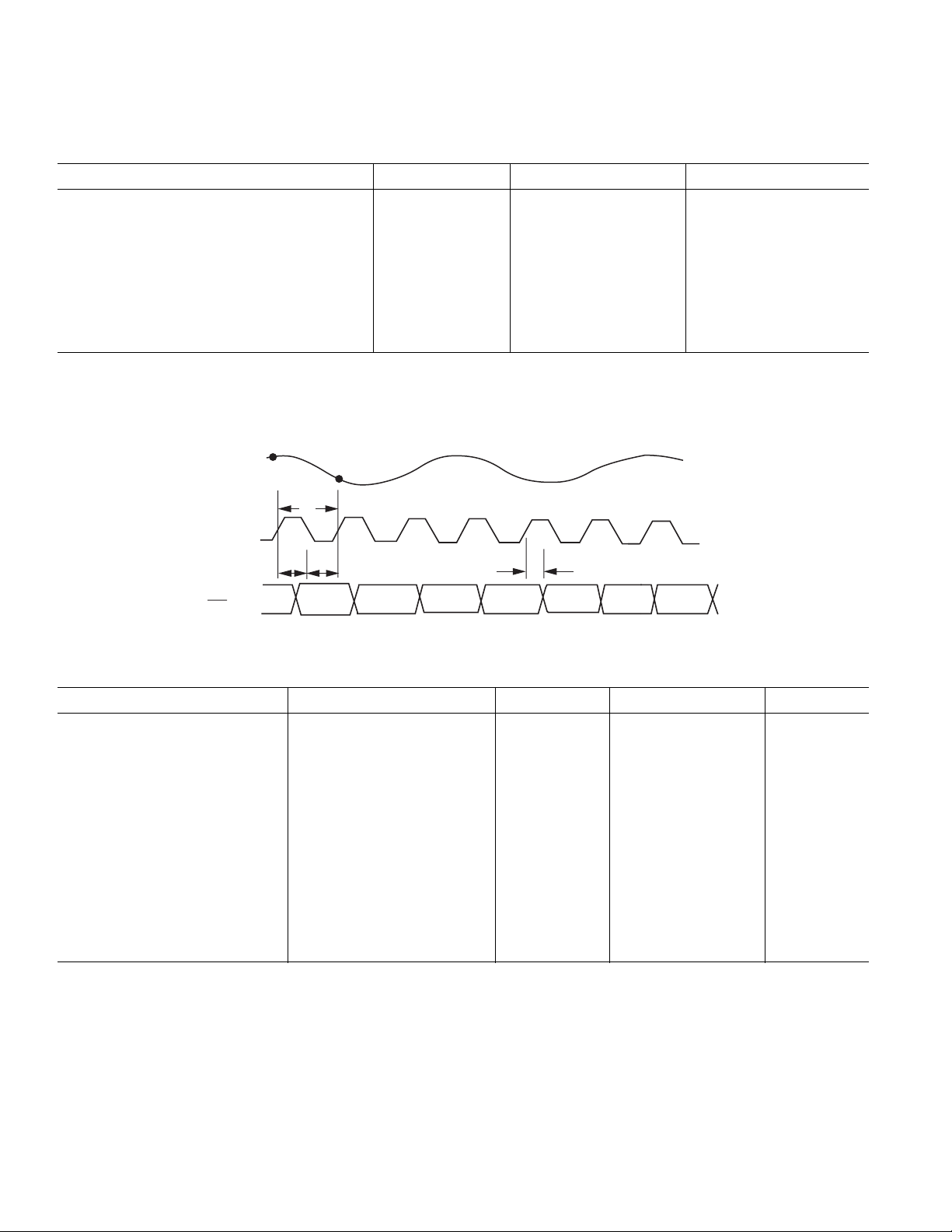
Clock Period
1
CLOCK Pulsewidth High t
CLOCK Pulsewidth Low t
Clock Duty Cycle
2
Output Delay t
Pipeline Delay (Latency) 3 Clock Cycles
Data Access Time (LCC Package Only)
Output Float Delay (LCC Package Only)
NOTES
1
Conversion rate is operational down to 10 kHz without degradation in specified performance.
2
See section on Three-State Outputs for timing diagrams and applications information.
Specifications subject to change without notice.
VIN
CLOCK
BIT 2–12
MSB, OTR
N
2
t
N
tCH t
2
N+1
C
N+1
CL
with AVDD = +5 V, DVDD = +5 V, DRVDD = +5 V, AVSS = –5 V; VIL = 0.8 V,
MAX
t
C
CH
CL
100 ns min
45 ns min
45 ns min
40 % min (50% typ)
60 % max
OD
t
DD
t
HL
DATA
N
10 ns min (20 ns typ)
50 ns typ (100 pF Load)
50 ns typ (10 pF Load)
t
OD
DATA
N+1
Figure 1. Timing Diagram
ABSOLUTE MAXIMUM RATINGS
1
Parameter With Respect to Min Max Units
AV
DD
AV
SS
DV
DRV
, DRV
DD
DD
2
DD
2
AGND –0.5 +6.5 Volts
AGND –6.5 +0.5 Volts
DGND, DRGND
DV
DD
2
–0.5 +6.5 Volts
–6.5 +6.5 Volts
DRGND DGND –0.3 +0.3 Volts
AGND DGND –1.0 +1.0 Volts
AV
DD
Clock Input, OEN
2
DV
DD
DGND –0.5 DVDD + 0.5 Volts
Digital Outputs DGND –0.5 DV
, V
V
INA
, REF IN AGND –6.5 +6.5 Volts
INB
REF IN AGND AV
–6.5 +6.5 Volts
+ 0.3 Volts
DD
SS
AV
DD
Volts
Junction Temperature +150 °C
Storage Temperature –65 +150 °C
Lead Temperature (10 sec) +300 °C
NOTES
1
Stresses above those listed under Absolute Maximum Ratings may cause permanent damage to the device. This is a stress rating only; functional operation of the device
at these or any other conditions above those indicated in the operational sections of this specification is not implied. Exposure to absolute maximum ratings for extended
periods may affect device reliability.
2
LCC package only.
REV. A–4–

7
17
8
9
10
11
12
13
14
15
16
164044 4142432345
29
39
30
31
32
33
34
35
36
37
38
18 2819 20 21 22 23 24 25 26 27
AD872A
TOP VIEW
(NOT TO SCALE)
OTR
REF GND
MSB
AV
DD
AGND
DGND
AV
SS
AV
DD
V
INAVINB
CLK
REF IN
REF OUT
BIT 12 (LSB)
AV
SS
AGND
DRGND
DV
DD
BIT 11
BIT 10
BIT 9
BIT 8
BIT 7
BIT 6
BIT 5
BIT 4
BIT 3
BIT 2
DRV
DD
DRV
DD
DRGND
OEN
BIT 1 (MSB)
NC
NC
NC
NC
NC
NC
NC
NC
NC
NC
NC
NC = NO CONNECT
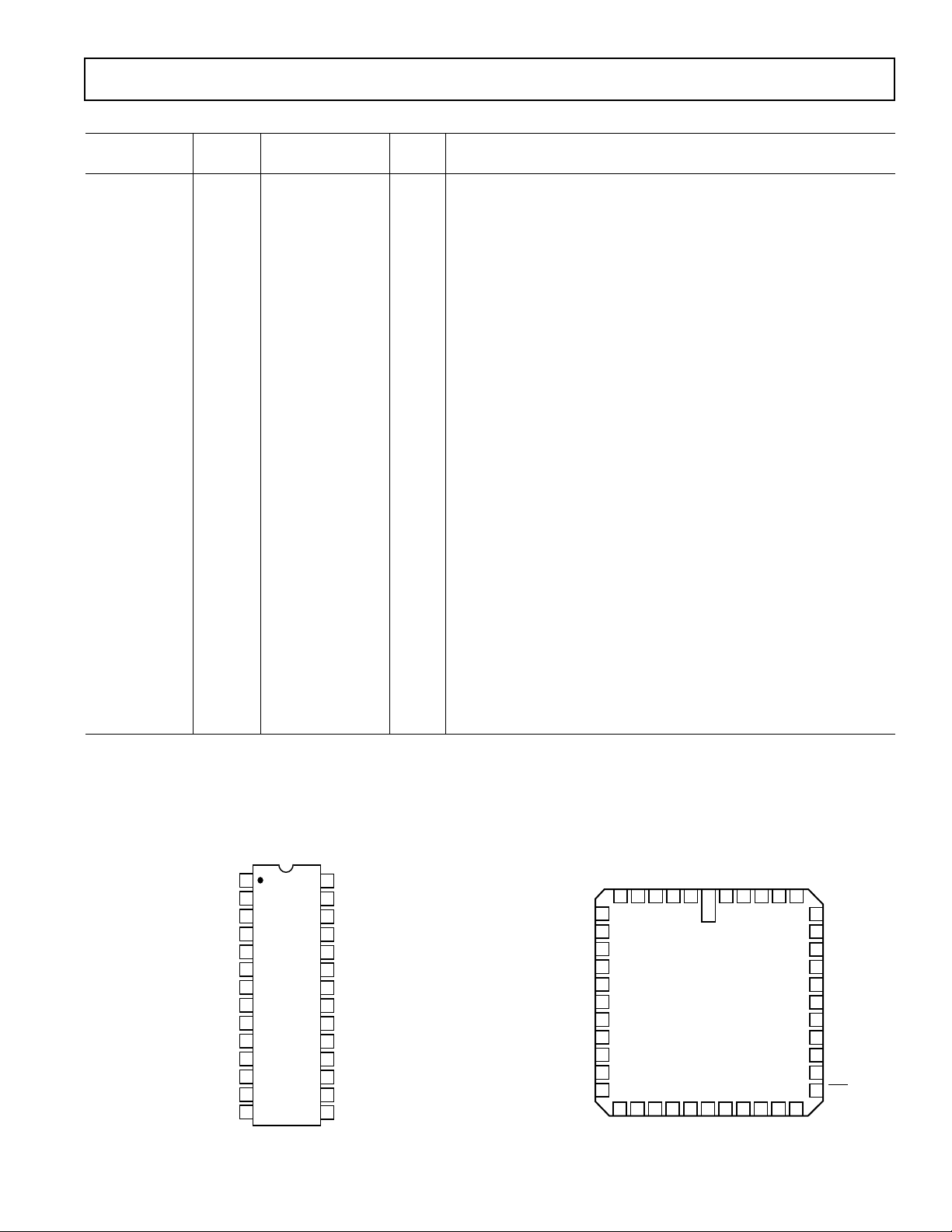
PIN DESCRIPTION
AD872A
Symbol Pin No. Pin No. Type Name and Function
DIP LCC
V
V
AV
AV
INA
INB
SS
DD
1 1 AI (+) Analog Input Signal on the differential input amplifier.
2 2 AI (–) Analog Input Signal on the differential input amplifier.
3, 25 5, 40 P –5 V Analog Supply.
4 6, 38 P +5 V Analog Supply.
AGND 5, 24 9, 36 P Analog Ground.
DGND 6, 23 10 P Digital Ground.
DV
DD
7, 22 33 P +5 V Digital Supply.
BIT 12 (LSB) 8 16 DO Least Significant Bit.
BIT 2–BIT 11 18–9 26–17 DO Data Bits 2 through 11.
MSB 19 29 DO Inverted Most Significant Bit. Provides twos complement output
data format.
OTR 20 30 DO Out of Range is Active HIGH on the leading edge of Code 0 or the
trailing edge of Code 4096. See Output Data Format Table III.
CLK 21 31 DI Clock Input. The AD872A will initiate a conversion on the rising
edge of the clock input. See the Timing Diagram for details.
REF OUT 26 41 AO +2.5 V Reference Output. Tie to REF IN for normal operation.
REF GND 27 42 AI Reference Ground.
REF IN 28 43 AI Reference Input. +2.5 V input gives ± 1 V full-scale range.
DRV
DD
N/A 12, 32 P +5 V Digital Supply for the output drivers.
NC N/A 3, 4, 7, 8, 14, 15, No Connect.
28, 35, 37, 39, 44
DRGND N/A 11, 34 P Digital Ground for the output drivers. (See section on Power Supply
Decoupling for details on DRV
and DRGND.)
DD
OEN N/A 13 DI Output Enable. See the Three State Output Timing Diagram for details.
BIT 1 N/A 27 DO Most Significant Bit.
TYPE: AI = Analog Input; AO = Analog Output; DI = Digital Input; DO = Digital Output; P = Power; N/A = Not Available on 28-lead DIP. Only available on
44-terminal surface mount package.
PIN CONFIGURATIONS
28-Lead Ceramic DIP 44-Terminal LCC
1
V
INA
V
2
INB
AV
3
REV. A –5–
AV
AGND
DGND
DV
BIT 12 (LSB)
BIT 11
BIT 10
BIT 9
BIT 8
BIT 7
BIT 6
SS
DD
DD
4
5
AD872A
6
TOP VIEW
(Not to Scale)
7
8
9
10
11
12
13
14
28
27
26
25
24
23
22
21
20
19
18
17
16
15
REF IN
REF GND
REF OUT
AV
SS
AGND
DGND
DV
DD
CLK
OTR
MSB
BIT 2
BIT 3
BIT 4
BIT 5

AD872A
DEFINITIONS OF SPECIFICATIONS
LINEARITY ERROR (INL)
Linearity error refers to the deviation of each individual code
from a line drawn from “negative full scale” through “positive
full scale.” The point used as “negative full scale” occurs
1/2 LSB before the first code transition. “Positive full scale” is
defined as a level 1 1/2 LSB beyond the last code transition.
The deviation is measured from the middle of each particular
code to the true straight line.
DIFFERENTIAL LINEARITY ERROR (DNL, NO MISSING
CODES)
An ideal ADC exhibits code transitions that are exactly 1 LSB
apart. DNL is the deviation from this ideal value. Guaranteed
no missing codes to 12-bit resolution indicates that all 4096
codes must be present over all operating ranges.
ZERO ERROR
The major carry transition should occur for an analog value
1/2 LSB below analog common. Zero error is defined as the
deviation of the actual transition from that point. The zero error
and temperature drift specify the initial deviation and maximum
change in the zero error over temperature.
GAIN ERROR
The first code transition should occur for an analog value
1/2 LSB above nominal negative full scale. The last transition
should occur for an analog value 1 1/2 LSB below the nominal
positive full scale. Gain error is the deviation of the actual difference between first and last code transitions and the ideal difference between first and last code transitions.
OVERVOLTAGE RECOVERY TIME
Overvoltage recovery time is defined as that amount of time required for the ADC to achieve a specified accuracy after an
overvoltage (50% greater than full-scale range), measured from
the time the overvoltage signal reenters the converter’s range.
DYNAMIC SPECIFICATIONS
SIGNAL-TO-NOISE AND DISTORTION (S/N+D) RATIO
S/N+D is the ratio of the rms value of the measured input signal
to the rms sum of all other spectral components below the
Nyquist frequency, including harmonics but excluding dc. The
value for S/N+D is expressed in decibels.
TOTAL HARMONIC DISTORTION (THD)
THD is the ratio of the rms sum of the first six harmonic components to the rms value of the measured input signal and is expressed as a percentage or in decibels.
INTERMODULATION DISTORTION (IMD)
With inputs consisting of sine waves at two frequencies, fa and
fb, any device with nonlinearities will create distortion products,
of order (m + n), at sum and difference frequencies of mfa ±
nfb, where m, n = 0, 1, 2, 3 . . . . Intermodulation terms are
those for which m or n is not equal to zero. For example, the
second order terms are (fa + fb) and (fa – fb), and the third order terms are (2 fa + fb), (2 fa – fb), (fa + 2 fb) and (2 fb – fa).
The IMD products are expressed as the decibel ratio of the rms
sum of the measured input signals to the rms sum of the distortion terms. The two signals are of equal amplitude and the peak
value of their sums is –0.5 dB from full scale. The IMD products are normalized to a 0 dB input signal.
TEMPERATURE DRIFT
The temperature drift for zero error and gain error specifies the
maximum change from the initial (+25°C) value to the value at
T
or T
MIN
POWER SUPPLY REJECTION
MAX
.
The specifications show the maximum change in the converter’s
full scale as the supplies are varied from nominal to min/max
values.
APERTURE JITTER
Aperture jitter is the variation in aperture delay for successive
samples and is manifested as noise on the input to the A/D.
APERTURE DELAY
Aperture delay is a measure of the Track-and-Hold Amplifier
(THA) performance and is measured from the rising edge of the
clock input to when the input signal is held for conversion.
FULL-POWER BANDWIDTH
The full-power bandwidth is that input frequency at which the
amplitude of the reconstructed fundamental is reduced by 3 dB
for a full-scale input.
SPURIOUS FREE DYNAMIC RANGE
The difference, in dB, between the rms amplitude of the input
signal and the peak spurious signal.
ORDERING GUIDE
Model Temperature Range Package Option
1
AD872AJD 0°C to +70°C D-28
AD872AJE 0°C to +70°C E-44A
AD872ASD
AD872ASE
NOTES
1
D = Ceramic DIP, E = Leadless Ceramic Chip Carrier.
2
MIL-STD-883 version will be available; contact factory.
2
–55°C to +125°C D-28
2
–55°C to +125°C E-44A
REV. A–6–
 Loading...