

Low Cost, Low Power,
G
FEATURES
Computes true rms value instantly
Accuracy: ±10 μV ± 0.5% of reading
Wide dynamic input range
100 μV rms to 3 V rms (8.5 V p-p) full-scale input range
Larger inputs with external scaling
Wide bandwidth:
1 MHz for −3 dB (300 mV)
65 kHz for additional 1% error
Zero converter dc output offset
No residual switching products
Specified at 300 mV rms input
Accurate conversion with crest factors up to 10
Low power: 300 µA typical at ±2.4 V
Fast settling at all input levels
High-Z FET separately powered input buffer
R
≥ 1012 Ω, CIN ≤ 2 pF
IN
Precision dc output buffer
Wide supply range
Dual: ±2.4 V to ±18 V
Single: 4.8 V to 36 V
Small size: 4 mm × 4 mm package
ESD protected
GENERAL DESCRIPTION
The AD8436 is a new generation, translinear precision, low power,
true rms-to-dc converter that is loaded with options. It computes
a precise dc equivalent of the rms value of ac waveforms, including
complex patterns such as those generated by switchmode power
supplies and triacs. Its accuracy spans a wide range of input levels
(see Figure 2) and temperatures. The ensured accuracy of ≤±0.5%
and ≤10 µV output offset result from the latest Analog Devices,
Inc., technology. The crest factor error is <0.5% for CF values
between 1 and 10.
The AD8436 delivers instant true rms results at less cost than
misleading peak, averaging, or digital solutions. There is no
programming expense or processor overhead to consider, and the
4 mm × 4 mm package easily fits into those tight applications.
On-board buffer amplifiers enable the widest range of options
for any rms-to-dc converter available, regardless of cost. For
minimal applications, only a single external averaging capacitor
is required. The built-in high impedance FET buffer provides an
interface for external attenuators, frequency compensation, or
driving low impedance loads. A matched pair of internal resistors
enables an easily configurable gain-of-two or more, extending
the usable input range even lower. The low power, precision input
buffer makes the AD8436 attractive for use in portable multi-
Rev. 0
Information furnished by Analog Devices is believed to be accurate and reliable. However, no
responsibility is assumed by Anal og Devices for its use, nor for any infringements of patents or ot her
rights of third parties that may result from its use. Specifications subject to change without notice. No
license is granted by implication or otherwise under any patent or patent rights of Analog Devices.
Trademarks and registered trademarks are the property of their respective owners.
True RMS-to-DC Converter
AD8436
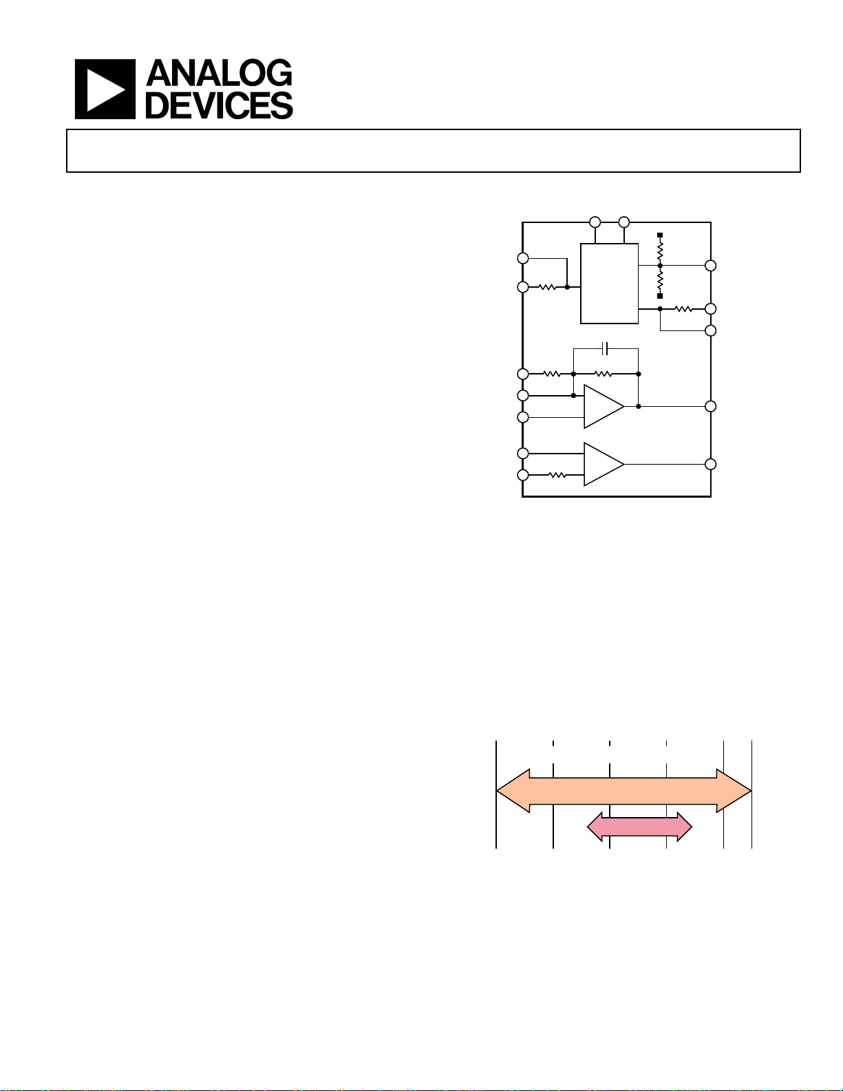
FUNCTIONAL BLOCK DIAGRAM
CAV
CCF
VCC
SUM
RMS
IBUFGN
IBUFIN–
IBUFIN+
OBUFIN+
OBUFIN–
8k
10k 10k
16k
RMS CORE
10pF
–
+
+
–
Figure 1.
meters and other battery-powered applications. The precision
dc output buffer offers extremely low offset voltages, thanks to
bias current cancellation.
Unlike digital solutions, the AD8436 has no switching circuitry
limiting performance at high or low amplitudes (see Figure 2).
A usable response of <100 µV and >3 V extends the dynamic
range with no external scaling, accommodating the most
demanding low signal conditions.
GREATER INPUT DYNAMIC RANGE
AD8436
SOLUTION
100µV 3V
1mV 10mV 1V100mV
Figure 2. Usable Dynamic Range of the AD8436 vs.
The AD8436 operates from single or dual supplies of ±2.4 V
(4.8 V) to ±18 V (36 V). A and J grades are available in a compact
4 mm × 4 mm, 20-lead chip-scale package. The operating
temperature ranges are −40°C to 125°C and 0°C to 70°C.
One Technology Way, P.O. Box 9106, Norwood, MA 02062-9106, U.S.A.
Tel: 781.329.4700 www.analog.com
Fax: 781.461.3113 ©2011 Analog Devices, Inc. All rights reserved.
100k
100k
VEE
FET OP AMP
DC BUFFER
AD8436
16k
IGND
OGND
OUT
IBUFOUT
OBUFOUT
ΔΣ
10033-001
10033-002

AD8436
TABLE OF CONTENTS
Features.............................................................................................. 1
Functional Block Diagram .............................................................. 1
General Description ......................................................................... 1
Revision History ............................................................................... 2
Specifications..................................................................................... 3
Absolute Maximum Ratings............................................................ 4
Thermal Resistance ...................................................................... 4
ESD Caution.................................................................................. 4
Pin Configuration and Function Descriptions............................. 5
Typical Performance Characteristics ............................................. 6
REVISION HISTORY
7/11—Revision 0: Initial Version
Test Circuits........................................................................................9
Theory of Operation ...................................................................... 10
Overview ..................................................................................... 10
Applications Information.............................................................. 12
Using the AD8436....................................................................... 12
AD8436 Evaluation Board......................................................... 16
Outline Dimensions....................................................................... 18
Ordering Guide .......................................................................... 18
Rev. 0 | Page 2 of 20

AD8436
SPECIFICATIONS
eIN = 300 mV ac (rms), frequency = 1 kHz sinusoidal, ac-coupled, ±VS = ±5 V, TA = 25°C, C
Table 1.
Parameter Test Conditions/Comments Min Typ Max Unit
RMS CORE
Conversion Error Default conditions ±10 − 0.5 ±0 ± 0 ±10 + 0.5 μV/% rdg
Vs. Temperature −40°C < T < 125 C 0.006 %/°C
Vs. Rail Voltage ±2.4 V to ±18 V ±0.013 ±%/V
Input Offset Voltage DC-coupled −500 0 +500 μV
Output Offset Voltage Default conditions, ac-coupled input 0 V
Vs. Temperature −40 C < T < 125°C 0.3 μV/°C
DC Reversal Error DC-coupled, VIN = ±300 mV ±0.5 ±2 %
Nonlinearity eIN = 10 mV to 300 mV ac (rms) 0.05 %
Crest Factor Error Additional error
1 < CF < 10 CCF = 0.1 μF −0.5 +0.5 %
Peak Input Voltage −VS − 0.7 +VS + 0.7 V
Input Resistance 7.92 8 8.08 kΩ
Frequency Response VIN = 300 mV rms
1% Additional Error 65 kHz
3 dB Bandwidth 1 MHz
Settling Time
0.1% Rising/falling 148/341 ms
0.01% Rising/falling 158/350 ms
Output Resistance 15.68 16 16.32 kΩ
Supply Current No input 325 400 μA
INPUT BUFFER
Signal Voltage Swing G = 1
Input AC- or dc-coupled −VS +VS V
Output AC-coupled to Pin RMS −VS + 0.2 +VS − 0.2 mV
Offset Voltage −1 0 +1 mV
Input Bias Current 50 pA
Input Resistance 1012 Ω
Frequency Response
0.1 dB 950 kHz
3 dB Bandwidth 2.1 MHz
Supply Current 100 160 200 μA
Optional Gain Resistor −9.9 +10 +10.1 kΩ
Gain Error G = ×1 0.05 %
OUTPUT BUFFER
Offset Voltage Connected to Pin OUT −200 0 +200 μV
Input Current 3 nA
Output Voltage Swing −VS + 0.0005 +VS − 1 V
Gain Error 0.003 0.01 %
Supply Current 40 70 μA
SUPPLY VOLTAGE
Dual ±2.4 ±18 V
Single 4.8 36 V
= 10 µF, unless otherwise specified.
AVG
Rev. 0 | Page 3 of 20
AD8436
ABSOLUTE MAXIMUM RATINGS
Table 2.
Parameter Rating
Supply Voltage ±18 V
Internal Power Dissipation 18 mW
Input Voltage ±VS
Output Short-Circuit Duration Indefinite
Differential Input Voltage +VS and −VS
Temperature
Operating Range −40°C to +125°C
Storage Range −65°C to +125°C
Lead Soldering (60 sec) 300°C
ESD Rating 2 kV
Stresses above those listed under Absolute Maximum Ratings
may cause permanent damage to the device. This is a stress
rating only; functional operation of the device at these or any
other conditions above those indicated in the operational
section of this specification is not implied. Exposure to absolute
maximum rating conditions for extended periods may affect
device reliability.
THERMAL RESISTANCE
θJA is specified for the worst-case conditions, that is, a device
soldered in a circuit board for surface-mount packages.
Table 3. Thermal Resistance
Package Type θJA Unit
CP-20-10 LFCSP Without Thermal Pad 86 °C/W
CP-20-10 LFCSP With Thermal Pad 48 °C/W
ESD CAUTION
Rev. 0 | Page 4 of 20
AD8436
VCC
2
M
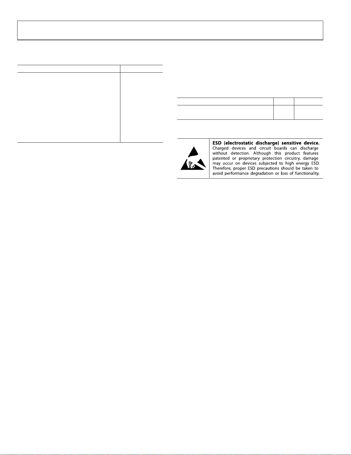
PIN CONFIGURATION AND FUNCTION DESCRIPTIONS
SU
CAVG
CCF
1
DNC
PIN 1
RMS
IBUFOUT
IBUFIN–
IBUFIN+
5
IBUFGN
NOTES
1. DNC = DO NOT CONNECT. DO NOT CONNECT TO THIS PIN.
. THE EXPOSED PAD SHOULD NOT BE CONNECTED.
INDICATOR
AD8436
TOP VIEW
(Not to S cale)
OGND
Figure 3. Pin Configuration, Top View
Table 4. Pin Function Descriptions
Pin No. Mnemonic Description
1 DNC Do Not Connect. Used for factory test.
2 RMS AC Input to the RMS Core.
3 IBUFOUT Output Connection for the FET Input Buffer Amplifier.
4 IBUFIN– Inverting Input to the FET Input Buffer Amplifier.
5 IBUFIN+ Noninverting Input to the FET Input Buffer Amplifier.
6 IBUFGN Optional 10 kΩ Precision Gain Resistor.
7 DNC Do Not Connect. Used for factory test.
8 OGND
Internal 16 kΩ Current-to-Voltage Resistor. Connect to ground for voltage output at Pin 9; leave unconnected
for current output at Pin 9.
9 OUT Voltage or Current Output of the RMS Core.
10 VEE Negative Supply Rail.
11 IGND Half Supply Node. Leave open for single-supply operation.
12 OBUFIN+ Noninverting Input of the Optional Precision Output Buffer. OBUFIN+ is typically connected to OUT.
13 OBUFIN− Inverting Input of the Optional Precision Output Buffer. OBUFIN− is typically connected to OBUFOUT.
14 OBUFOUT Low Impedance Output for ADC or Other Loads.
15 OBUFV+ Power Pin for the Output Buffer.
16 IBUFV+ Power Pin for the Input Buffer.
17 VCC Positive Supply Rail for the RMS Core.
18 CCF Connection for Crest Factor Capacitor.
19 CAVG Connection for Averaging Capacitor.
20 SUM Summing Amplifier Input Node. An external resistor can be connected for custom scaling.
EP DNC Exposed Pad. The exposed pad should not be connected.
IBUFV+
1620
15
OBUFV+
OBUFOUT
OBUFIN–
OBUFIN+
IGND
11
106
VEE
OUTDNC
10033-003
Rev. 0 | Page 5 of 20
AD8436
V
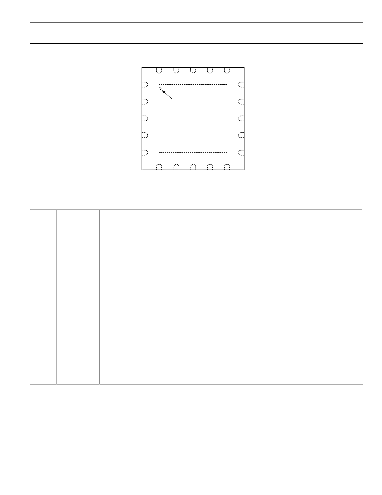
TYPICAL PERFORMANCE CHARACTERISTICS
TA = 25°C, ±VS = ±5 V, C
5V
= 10 µF, 1 kHz sine wave, unless otherwise indicated.
AVG
5
1V
100mV
10mV
INPUT LEVEL (V rms)
1mV
100µV
50µV
100 1k
FREQUENCY (Hz)
Figure 4. RMS Core Frequency Response (See Figure 20)
5V
1V
100mV
10mV
INPUT LEVEL (V rms)
1mV
100µV
50µV
100 1k
FREQUENCY ( Hz)
Figure 5. RMS Core Frequency Response with V
3dB BW
100k10k
3dB BW
VS = ±2.4V
100k10k
= ±2.4 V (See Figure 20)
S
5M1M50
1V
100mV
10mV
INPUT LEVEL (V rms)
1mV
100µV
50µV
5M1M50
10033-004
100 1k
FREQUENCY (Hz)
Figure 7. RMS Core Frequency Response with V
15
e
= 3.5mV rms
IN
12
9
6
3
0
GAIN (dB)
–3
–6
–9
–12
–15
100 1k
10033-005
FREQUENCY (Hz)
100k10k
3dB BW
VS = 4.8V
100k10k
= +4.8 V (See Figure 21)
S
5M1M50
5M1M
10033-007
10033-008
Figure 8. Input Buffer, Small Signal Bandwidth at 0 dB and 6 dB Gain
5V
1V
100mV
10mV
INPUT LEVEL (V rms)
1mV
100µV
50µV
100 1k
FREQUENCY ( Hz)
Figure 6. RMS Core Frequency Response with V
3dB BW
VS = ±15V
100k10k
= ±15 V (See Figure 20)
S
5M1M50
10033-006
15
e
= 300mV rms
IN
12
9
6
3
0
GAIN (dB)
–3
–6
–9
–12
–15
100 1k
FREQUENCY (Hz)
100k10k
5M1M
Figure 9. Input Buffer, Large Signal Bandwidth at 0 dB and 6 dB Gain
10033-009
Rev. 0 | Page 6 of 20

AD8436
15
e
= 3.5mV rms
IN
12
9
6
3
0
GAIN (dB)
–3
–6
–9
–12
–15
100 1k
FREQUENCY (Hz)
Figure 10. Output Buffer, Small Signal Bandwidth
100k10k
5M1M
10033-010
10
PW = 100µs
5
CAVG = 10µF
0
−5
ADDITIO NAL ERROR (% OF READI NG)
−10
20
CREST FACTOR RATIO
CCF = 0.1µF
64
CAVG = 10µF
810
Figure 13. Crest Factor Error vs. Crest Factor for CAVG and CAVG and CCF
10033-013
Capacitor Combinations
1.00
0.75
0.50
0.25
0
−0.25
−0.50
ADDITIONAL ERROR (% OF READING)
−0.75
−1.00
–25–50
TEMPERAT URE (°C)
50
250
Figure 14. Additional Conversion Error vs. Temperature
75
100 125
10033-014
NORMALIZED ERROR (%)
0.5
0.4
0.3
0.2
0.1
–0.1
–0.2
–0.3
–0.4
–0.5
CAVG = 10µF
8 SAMPLES
0
0
8426 141210
SUPPLY VOLTAGE (±V)
Figure 11. Additional Error vs. Supply Voltage
20
1816
10033-011
2.0
1.6
1.2
0.8
INPUT LEVEL (V rms)
0.4
0
0
46
SUPPLY VOLTAGE (±V)
108
14122
Figure 12. Core Input Voltage for 1% Error vs. Supply Voltage
2.5
2.0
1.5
1.0
SUPPLY CURRENT (mA)
0.5
0
16
18
10033-012
0
V
= ±5V
S
0.5 1.0
INPUT VOLTAGE (V rms)
Figure 15. RMS Core Supply Current vs. Input for V
VS = ±15V
VS = ±2.4V
2.01.5
= ±2.4 V, ±5 V, and ±15 V
S
10033-015
Rev. 0 | Page 7 of 20

AD8436
90
80
70
60
50
40
30
BIAS CURRENT (pA)
20
10
0
10
2550
250
TEMPERATURE (°C)
7550
100 125
10033-016
INPUT OFFSET VOLTAGE (µV)
250
200
150
100
50
100
150
200
250
50
0
2550
250
TEMPERAT URE (°C)
7550
100 125
10033-019
Figure 16. FET Input Buffer Bias Current vs. Temperature
1000
750
500
250
0
250
500
INPUT OFFSET VOLTAGE (µV)
750
1000
2550
250
TEMPERAT URE (°C)
7550
Figure 17. Input Offset Voltage of FET Buffer vs. Temperature
100 125
Figure 18. Output Buffer V
1kHz 300mV rms BURST INPUT
300mV DC OUT
1kHz 1mV rms BURST INPUT
1mV DC OUT
10033-018
TIME (50ms/ DIV)
vs. Temperature
OS
CAVG = 10µF
0V
0V
0V
0V
10033-020
Figure 19. Transition Times with 1 kHz Burst at Two Input Levels
(See Theory of Operation Section)
Rev. 0 | Page 8 of 20

AD8436
V
F
TEST CIRCUITS
SIGNAL S OURCE
CAV VCC
4.7µF
RMS
AC-IN MONI TOR
PRECISION DMM
OUT
PRECISION DMM
RMS CORE
16k
OGND
Figure 20. Core Response Test Circuit Using Dual Supplies
SIGNAL S OURCE
CAV VCC
4.7µF
RMS
AC-IN MONIT OR
PRECISION DMM
OUT
RMS CORE
16k
OGND
+5V10µF
100k
IGND
100k
VEE
–5V
10033-021
4.80V10µF
100k
IGND
100k
VEE
4.7µF
PRECISION DMM
10033-022
Figure 21. Core Response Test Circuit Using a Single Supply
+5
FUNCTION GENERATO R
AC-IN MONITOR
PRECISION DMM
PRECISION DMM
RMS
4.7µF
OUT
16k
OGND
10µ
CAV VCC
RMS CORE
–5V
100k
100k
VEE
IGND
10033-023
Figure 22. Crest Factor Test Circuit
Rev. 0 | Page 9 of 20

AD8436
V
THEORY OF OPERATION
OVERVIEW
The AD8436 is an implicit function rms-to-dc converter that
renders a dc voltage dependent on the rms (heating value) of an
ac voltage. In addition to the basic converter, this highly integrated
functional circuit block includes two fully independent, optional
amplifiers, a standalone FET input buffer amplifier and a precision
dc output buffer amplifier (see Figure 1). The rms core includes
a precision current responding full-wave rectifier and a log-antilog
transistor array for current squaring and square rooting to implement the classic expression for rms (see Equation 1). For basic
applications, the converter requires only an external capacitor, for
averaging (see Figure 30). The optional on-board amplifiers
offer utility and flexibility in a variety of applications without
incurring additional circuit board footprint. For lowest power,
the amplifier supply pins are left unconnected.
Why RMS?
The rms value of an ac voltage waveform is equal to the dc voltage
providing the same heating power to a load. A common measurement technique for ac waveforms is to rectify the signal in a
straightforward way using a diode array of some sort, resulting in
the average value. The average value of various waveforms (sine,
square, and triangular, for example) varies widely; true rms is
the only metric that achieves equivalency for all ac waveforms.
See Tab l e 5 for non-rms-responding circuit errors.
The acronym “rms” means root-mean-square and reads as follows:
“the square root of the average of the sum of the squares” of the
peak values of any waveform. RMS is shown in the following
equation:
For additional information, select Section I of the 2
the Analog Devices RMS-to-DC Applications Guide.
RMS Core
The core consists of a voltage-to-current converter (precision
resistor), absolute value, and translinear sections. The translinear
section exploits the properties of the bipolar transistor junctions
for squaring and root extraction (see Figure 23). The external
capacitor (CAVG) provides for averaging the product. Figure 19
shows that there is no effect of signal input on the transition times,
as seen in the dc output. Although the rms core responds to input
voltages, the conversion process is current sensitive. If the rms
input is ac-coupled, as recommended, there is no output offset
voltage, as reflected in Ta ble 1 . If the rms input is dc-coupled, the
input offset voltage is reflected in the output and can be calibrated
as with any fixed error.
+
CAVG
AC I N
V-TO-I
ABSOLUTE
VALUE
CIRCUIT
Figure 23. RMS Core Block Diagram
5k
V–
nd
edition of
–
+
V+
OUT
16k
10033-024
(1)
Table 5. General AC Parameters
Reading of an Average Value Circuit
Waveform Type (1 V p-p) Crest Factor RMS Value
Calibrated to an RMS Sine Wave Error (%)
Sine 1.414 0.707 0.707 0
Square 1.00 1.00 1.11 11.0
Triangle 1.73 0.577 0.555 −3.8
Noise 3 0.333 0.295
Rectangular 2 0.5 0.278 −11.4
Pulse 10 0.1 0.011 −44
SCR −89
DC = 50% 2 0.495 0.354 −28
DC = 25% 4.7 0.212 0.150 −30
Rev. 0 | Page 10 of 20
AD8436
The 16 k resistor in the output converts the output current to
a dc voltage that can be connected to the output buffer or to the
circuit that follows. The output appears as a voltage source in
series with 16 k. If a current output is desired, the resistor
connection to ground is left open and the output current is
applied to a subsequent circuit, such as the summing node of
a current summing amplifier. Thus, the core has both current
and voltage outputs, depending on the configuration. For a
voltage output with 0 source impedance, use the output
buffer. The offset voltage of the buffer is 25 V or 50 V,
depending on the grade.
FET Input Buffer
Referring to Figure 1, the input resistance of the AD8436 is 8 kΩ,
and a voltage source input is preferred. The optional input buffer
is a wideband JFET input amplifier that minimally loads non-0 Ω
sources, such as a tapped resistor attenuator or voltage sensor.
Although the input buffer consumes only 150 A, the supply is
pinned out and left unconnected to reduce power where needed.
Optional matched 10 kΩ input and feedback resistors are provided
on chip. Consult the Applications Information section to learn
how these resistors can be used. The 3 dB bandwidth of the input
buffer is 2.7 MHz at 10 mV rms input and approximately 1.5 MHz
at 1 V rms. The amplifier gain and bandwidth are sufficient for
applications requiring modest gain or response enhancement to
a few hundred kilohertz (kHz), if desired. Configurations of the
input buffer are discussed in the Applications Information
section.
Precision Output Buffer
The precision output buffer is a bipolar input amplifier, laser
trimmed to cancel input offset voltage errors. As with the input
buffer, the supply current is very low (<50 A, typically), and the
power can be disconnected for power savings if the buffer is not
needed. Be sure that the noninverting input is also disconnected
from the core output (OUT) if the buffer supply pin is disconnected. Although the input current of the buffer is very low,
a laser-trimmed 16 k resistor, connected in series with the
inverting input, offsets any self-bias offset voltage.
The output buffer can be configured as a single or two-pole lowpass filter using circuits shown in the Applications Information
section. Residual output ripple is reduced, without affecting the
converted dc output. As the response approaches the low
frequency end of the bandwidth, the ripple rises, dependent on
the value of the averaging capacitor. Figure 26 shows the effects of
four combinations of averaging and filter capacitors. Although
the filter capacitor reduces the ripple for any given frequency, the
dc error is unaffected. Of course, a larger value averaging
capacitor can be selected, at a larger cost. The advantage of using
a low-pass filter is that a small value of filter capacitor, in
conjunction with the 16 kΩ output resistor, reduces ripple and
permits a smaller averaging capacitor, effecting a cost savings.
The recommended capacitor values for operation to 40 Hz are
10 µF for averaging and 3.3 µF for filter.
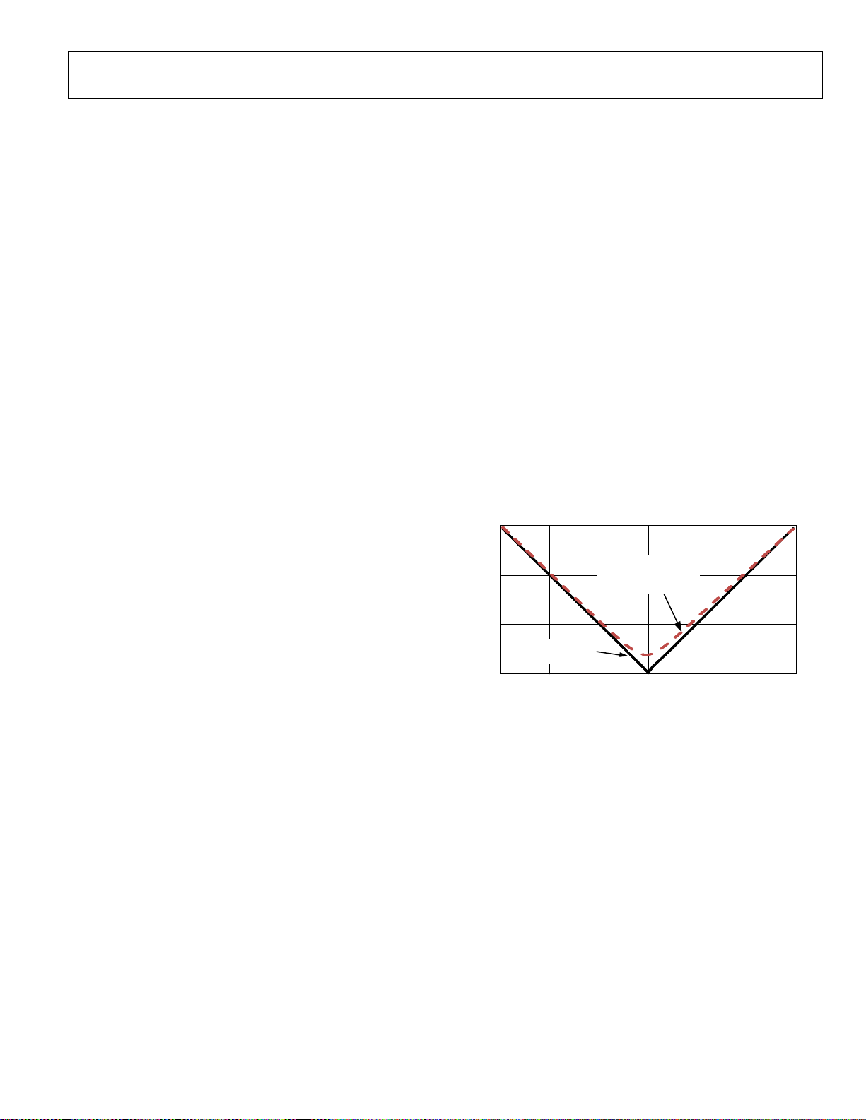
Dynamic Range
The AD8436 is a translinear rms-to-dc converter with exceptional
dynamic range. Although accuracy varies slightly more at the
extreme input values, the device still converts with no spurious
noise or dropout. Figure 24 is a plot of the rms/dc transfer function
near zero voltage. Unlike processor or other solutions, residual
errors at very low input levels can be disregarded for most
applications.
30
OR OTHER DIG ITAL
SOLUTI ONS CANNOT
WORK AT Z ERO
VOLTS
INPUT VOLTAGE (mV DC)
0
302010–10–20–30
OUTPUT V OLTAG E (mV DC)
20
10
AD8436
SOLUTION
0
Figure 24. DC Transfer Function near Zero
10033-025
Rev. 0 | Page 11 of 20

AD8436
C
R
APPLICATIONS INFORMATION
USING THE AD8436
This section describes the power supply and feature options,
as well as the function and selection of averaging and filter
capacitor values. Averaging and filtering options are shown
graphically and apply to all circuit configurations.
Averaging Capacitor Considerations—RMS Accuracy
Ty pi ca l AD8436 applications require only a single external
capacitor (CAVG) connected to the CAVG pin (see Figure 30).
The function of the averaging capacitor is to compute the mean
(that is, average value) of the sum of the squares. Averaging
(that is, integration) follows the absolute value circuit, where
the polarity of negative input current components is reversed
(rectified) prior to squaring. The mean value is the average
value of the squared input voltage over several input waveform
periods. The rms error is directly affected by the number of
periods averaged, as is the resultant peak-to-peak ripple.
The result of the conversion process is a dc component and a
ripple component whose frequency is twice that of the input. The
rms conversion accuracy depends on the value of CAVG, so the
value selected need only be large enough to average enough periods
at the lowest frequency of interest to yield the required rms
accuracy. Figure 27 is a plot of rms error vs. frequency for various
averaging capacitor values. For Figure 27, the additional error
was 0.001% at 40 Hz using a 10 µF metalized polyester capacitor.
Larger values yield diminished returns because the settling time
increases with negligible improvement in rms accuracy.
To u s e Figure 27, determine the minimum operating frequency
and accuracy of the application and then find the suggested
capacitor value on the chart. For example, for –0.5% rms at 100 Hz,
the capacitor value is 1 µF.
Post Conversion Ripple Reduction Filter
Input rectification included in the AD8436 introduces a
residual ripple component that is dependent on the value
of CAVG and twice the input signal frequency. For sampling
applications such as a high resolution ADC, the ripple component
may cause one or more LSBs to cycle, and low value display
numerals to flash.
0
22µF
10µF
–0.5
47µF
Ripple is reduced by increasing the value of the averaging capacitor,
or by postconversion filtering. Ripple reduction following
conversion is far more efficient because the ripple average value
has been converted to its rms value. Capacitor values for postconversion filtering are significantly less than the equivalent
averaging capacitor value for the same level of ripple reduction.
This approach requires only a single capacitor connected to the
OUT pin (see Figure 25). The capacitor value correlates to the
simple frequency relation of ½ π R-C, where R is fixed at 16 kΩ.
OGND
8
OUT
16k
CLPF
DC OUTPUT
10033-026
9
CORE
Figure 25. Simple One-Pole Post Conversion Filter
As seen in Figure 26, CAVG alone determines the rms error,
and CLPF serves purely to reduce ripple. Figure 26 shows a
constant rms error for CLPF values of 0.33 µF and 3.3 µF; only
the ripple is affected.
1
0
–1
–2
–3
–4
–5
–6
RMS ERROR (%)
–7
–8
–9
–10
10
Figure 26. RMS Error vs. Frequency for Two Values of CAVG and CLPF
CAVG = 10µF
CLPF = 0.33µF OR 3.3µF
CAVG = 1µF
CLPF = 0. 33µF O R 3.3µF
100 1k
FREQUENCY (Hz)
(Compare the effects of CAVG and CLPF, and
note that CLPF does not affect rms error result.)
10033-027
ROR (%)
–1.0
4.7µF
–1.5
ONVERSION E
–2.0
10
2.2µF
Figure 27. Conversion Error vs. Frequency for Various Values of CAVG
1µF
FREQUENCY (Hz )
Rev. 0 | Page 12 of 20
100
0.47µF
CAVG = 0. 22µF
1k
10033-028

AD8436
G
G
For simplicity, Figure 28 shows ripple vs. frequency for four
combinations of CAVG and CLPF
1
0.1
0.01
RIPPLE ERROR (V p-p)
0.001
0.0001
Figure 28. Residual Ripple Voltage for Various Filter Configurations
AC INPUT = 300mV rms
CAVG = 1µF, CLPF = 0.33µF
CAVG = 1µF, CLPF = 3. 3µF
CAVG = 10µF, CLPF = 0.33µF
CAVG = 10µF, CLPF = 3.3µF
100 1k10
INPUT FREQUENCY (Hz)
10033-029
Figure 29 shows the effects of averaging and post-rms filter
capacitors on transition and settling times using a 10-cycle,
50 Hz, 1 second period burst signal input to demonstrate timedomain behavior. In this instance, the averaging capacitor value
was 10 µF, yielding a ripple value of 6 mV rms. A postconversion
capacitor (CLPF) of .068 F reduced the ripple to 1 mV rms. An
averaging capacitor value of 82 F reduced the ripple to 1 mV
but extended the transition time (and cost) significantly.
INPUT
50Hz 10 CYCLE BURST
400mV/DIV
CAVG = 10µF FOR BOT H
PLOTS, BUT RED PLO T HAS
NO LOW-PASS FILTER, G REEN
PLOT HAS CLPF = 68nF 100mV/DIV
CAVG = 82µF
TIME (100ms/ DIV)
10033-030
Figure 29. Effects of Various Filter Options on Transition Times
Capacitor Construction
Although tolerant of most capacitor styles, rms conversion
accuracy can be affected by the type of capacitor that is selected.
Capacitors with low dc leakage yield best all around performance,
and many sources are available. Metalized polyester or similar
film styles are best, as long as the temperature range is appropriate.
For practical applications such as the rms-to-dc function in
DMMs or power monitoring circuits, surface mount tantalums
are the best over-all choice.
Basic Core Connections
Many applications require only a single external capacitor for
averaging. A 10 µF capacitor is more than adequate for acceptable
rms errors at line frequencies and below.
The signal source sees the input 8 k voltage-to-current conversion
resistor at Pin 2 (RMS); thus, the ideal source impedance is a
voltage source (0 source impedance). If a non-zero signal source
impedance cannot be avoided, be sure to account for any series
connected voltage drop.
An input coupling capacitor must be used to realize the near-zero
output offset voltage feature of the AD8436. Select a coupling
capacitor value that is appropriate for the lowest expected
operating frequency of interest. As a rule of thumb, the input
coupling capacitor can be the same as or half the value of the
averaging capacitor because the time constants are similar. For
a 10 F averaging capacitor, a 4.7 F or 10 F tantalum capacitor
is a good choice (see Figure 30).
CAV
4.7µF
OR
10µF
10µF
19
CAVG VCC
AD8436
2
RMS
VEE
IGND
11 10 8
–5V
Figure 30. Basic Applications Circuit
17
OUT
OGND
+5V
9
10033-031
Using a Capacitor for High Crest Factor Applications
The AD8436 contains a unique crest factor feature. Crest factor
is often overlooked when considering the requirements of rmsto-dc converters, but it is very important when working with
signals with spikes or high peaks. The crest factor is defined as
the ratio of peak voltage to rms. See Tabl e 5 for crest factors for
some common waveforms.
CAV
10µF
4.7µF
OR
10µF
19 18
CAVG CCF VCC
AD8436
2
RMS
VEE
IGND
11 10 8
–5V
Figure 31. Connection for Additional Crest Factor Performance
CCF
0.1µF
17
OUT
OGND
+5V
9
10033-032
Crest factor performance is mostly applicable for unexpected
waveforms such as switching transients in switchmode power
supplies. In such applications, most of the energy is in these
peaks and can be destructive to the circuitry involved, although
the average ac value can be quite low.
Figure 13 shows the effects of an additional crest factor
capacitor of 0.1 F and an averaging capacitor of 10 F. The
larger capacitor serves to average the energy over long spaces
between pulses, while the CCF capacitor charges and holds the
energy within the relatively narrow pulse.
Rev. 0 | Page 13 of 20

AD8436
Using the FET Input Buffer
The on-chip FET input buffer is an uncommitted FET input
op amp used for driving the 8 kΩ I-to-V input resistor of the
rms core. Pin 3, Pin 4, and Pin 5 are the I/O, Pin 6 is an optional
connection for gain in the input buffer, and and Pin 16 connects
power to the buffer (see Figure 3 and Tabl e 4 for location and
description). Connecting Pin 16 to the positive rail is the only
power connection required because the negative rail is internally
connected. Because the input stage is a FET and the input
impedance must be very high to prevent loading of the source,
a large value (10 MΩ) resistor must be connected from midsupply
at Pin 11 (IGND) to Pin 5 (IBUFIN+) to prevent the input gate
from floating high.
For unity gain, connect Pin 3 (IBUFOUT) to Pin 4 (IBUFIN−).
For a gain of 2×, connect Pin 6 (IBUFGN) to ground. See Figure 8
and Figure 9 for large and small signal responses at the two
built-in gain options.
The offset voltage of the input buffer is ≤500 V, depending on
grade. A capacitor connected between the Buffer Output Pin 3
(IBUFOUT) and Pin 2 (RMS) is recommended so that the input
buffer offset voltage does not contribute to the overall error.
Select the capacitor value for least minimum error at the lowest
operating frequency. Figure 32 is a schematic showing internal
components and pin connections.
RMS
10µF
0.47µF
10M
2
IBUFOUT
3
IBUFIN–
4
IBUFIN+
5
IGND
11
Figure 32. Connecting the FET Input Buffer
16
IBUFV+
10k
6
IBUFGN
–
+
10k
10pF
10033-033
Capacitor coupling at the input and output of the FET buffer is
recommended to avoid transferring the buffer offset voltage to
the output. Although the FET input impedance is extremely high,
the 10 M centering resistor connected to IGND must be taken
into account when selecting an input capacitor value. This is simply
an impedance calculation using the lowest desired frequency,
and finding a capacitor value based on the least attenuation desired.
Because the 10 k resistors are closely matched and trimmed to
a high tolerance, the input buffer gain can be increased to several
hundred with an external resistor connected to Pin 4 (IBUFIN−).
The bandwidth diminishes at the typical rate of a decade per 20 dB
of gain, and the output voltage range is constrained. The small
signal response, as shown in Figure 8, serves as a guide. As an
example, suppose one wanted to detect small input signals at power
line frequencies? An external 10 Ω resistor connected from Pin 4 to
ground sets the gain to 101 and the 3 dB bandwidth to ~30 kHz,
which is more than adequate for amplifying power line frequencies.
Using the Output Buffer
The AD8436 output is a precision op amp that is optimized
for dc operation. Figure 33 shows a block diagram of the basic
amplifier and I/O pins. The amplifier is intended for noninverting
operation only; note that the 16 k resistor, in series with the
inverting input of the amplifier, is used to balance the bias
current of the noninverting amplifier.
As with the input FET buffer, the amplifier positive supply is
pinned out separately for power sensitive applications. In normal
circumstances, the buffers are connected to the same supply as
the core. Figure 34 shows the signal connections to the output
buffer. Note that the input offset voltage contribution by the
bias currents are balanced by equal value series resistors,
resulting in near zero offset voltage.
OUTPUT BUFFER
OBUFIN+
OBUFIN–
16k
+
–
OBUFOUT
10033-034
Figure 33. Output Buffer Block Diagram
IBIAS
CORE
OGND
8
OUT
16k
9
IBIAS
OBUFIN+
12
13
OBUFIN–
16k
+
–
OBUFOUT
14
10033-035
Figure 34. Basic Output Buffer Connections
For applications requiring ripple suppression in addition to the
single-pole output filter described previously, the output buffer
is configurable as a two-pole Sallen-Key filter using two external
resistors and two capacitors. At just over 100 kHz, the amplifier
has enough bandwidth to function as an active filter for low
frequencies such as power line ripple. For a modest savings in
cost and complexity, the external 16 k feedback resistor can be
omitted, resulting in slightly higher V
2C
16k
C
Low-Pass Filter
OGND
OUT
16k
8
CORE
Figure 35. Output Buffer Amplifier Configured as a Two-Pole, Sallen-Key
OBUFIN+
129
13
OBUFIN–
(80 V).
OS
16k
16k
+
–
14
OBUFOUT
10033-036
Rev. 0 | Page 14 of 20

AD8436
F
A
V
Configure the output buffer as shown in Figure 36 to invert the
dc output.
CORE
OGND
OUT
16k
8
32.4k
Figure 36. Inverting Output Configuration
139
12
16k
OBUFIN–
OBUFIN+
–
+
14
OBUFOUT
Current Output Option
If a current output is required, connect the current output, OUT
(Pin 9), to the destination load. To maximize precision, provide
a means for external calibration to replace the internal trimmed
resistor, which is bypassed. This configuration is useful for convenient summing of the AD8436 result with another voltage, or
for polarity inversion.
CAVG
CCF
1819
DIRECTION OF
8k
2 9
RMS
16k
OGND
CORE
8
DC OUTPUT
CURRENT
DO NOT CONNECT F OR
CURRENT OUTPUT
OUT
16k
15k
–
+
2k
(OPTIONAL)
INVERTED DC
VOLTAGE
OUTPUT
10033-038
Figure 37. Connections for Current Output Showing Voltage Inversion
Single Supply
Connections for single supply operation are shown in Figure 38
and are similar to those for dual power supply when the device is
ac-coupled. The analog inputs are all biased to half the supply
voltage, but the output remains referred to ground because the
output of the AD8436 is a current source. An additional bypass
connection is required at Pin 11 (IGND) to suppress ambient noise.
10µ
19
CAV VCC
RMS
4.7µF
10033-037
0.47µF
10M
2
3
4
5
AD8436
IBUFOUT
IBUFIN–
IBUFIN+
OGND
8
17
VEE
10
OUT
IGND
9
11
4.7µF
10033-039
Figure 38. Connections for Single Supply Operation
Recommended Application
Figure 39 shows a circuit for a typical application for frequencies
as low as power line, and above. The recommended averaging,
crest factor and LPF capacitor values are 10 F, 0.1 F and
3.3 F. Refer to the Using the Output Buffer section if additional
low-pass filtering is required.
CC
10µF
0.1µF
+
OUTDNC
16
OBUFV+
OBUFOUT
OBUFIN–
OBUFIN+
IGND
VEE
10
VEE
15
14
DC
OUT
13
12
11
10033-040
C IN
10µF
0.47µF
10M
19 18 1720
SUM IBUFV+
CAVG VCC
CCF
1
DNC
2
RMS
3
IBUFOUT
4
IBUFIN–
5
IBUFIN+
AD8436
OGNDIBUFGN
8769
3.3µF
Figure 39. Typical Application Circuit
Rev. 0 | Page 15 of 20

AD8436
AD8436 EVALUATION BOARD
The AD8436-EVALZ provides a platform to evaluate AD8436
performance. The board is fully assembled, tested and ready to
use after the power and signal sources are connected. Figure 45
is a photograph of the board. Signal connections are located
on the primary and secondary sides, with power and ground
on the inner layers. Figure 40, Figure 41, Figure 42, Figure 43,
and Figure 44 illustrate the various design details of the board,
including a basic layout and copper patterns. These figures are
useful for reference for application designs.
A Word About Using the AD8436 Evaluation Board
The AD8436-EVALZ offers many options, without sacrificing
simplicity. The board is tested and shipped with a 10 μF averaging
capacitor (CAVG), 3.3 μF low-pass filter capacitor (C8) and a
0.1 μF (COPT) capacitor to optimize crest factor performance.
To evaluate minimum cost applications, remove C8 and COPT.
The functions of the five switches are listed in Table 6.
Table 6.
Switch Func tion
CORE_BUFFER Selects core or input for the input signal
INCOUP Selects ac or dc coupling to the core
SDCOUT
Selects the output buffer or the core
output at the DCOUT BNC.
IBUF_VCC Enable or disables the input buffer
OBUF_VCC Enable or disables the output buffer
All the I/Os are provided with test points for easy monitoring
with test equipment. The input buffer gain default is unity; for
2× gain, install a 0603 0 Ω resistor at Position R5. For higher
IBUF gains, remove the 0 Ω resistor at Position RFBH (there is
an internal 10 kΩ resistor from the OBUF_OUT to IBUFIN−)
and install a smaller value resistor in Position RFBL. A 100 Ω
resistor establishes a gain of 100×.
Single supply operation requires removal of Resistor R6 and
installing a 0.1 μF capacitor in the same position for noise
decoupling.
Figure 41. AD8436-EVALZ Primary Side Copper
Figure 42. AD8436-EVALZ Secondary Side Copper
Figure 43. AD8436-EVALZ Power Plane
10033-042
10033-043
10033-044
10033-045
Figure 44. AD8436-EVALZ Ground Plane
Figure 40. Assembly of the AD8436-EVALZ
10033-041
Rev. 0 | Page 16 of 20

AD8436
A
V
10033-046
Figure 45. Photograph of the AD8436-EVALZ
GND1
C IN
CORE_BUF
TACIN
C5
0.47µF
CORE
BUF
INCOUP
CIN
10µF
RFBH
0
RFBL
DNI
R1
1M
GND5GND4GND3GND2
DCAC
TRMSIN
TIBUFOUT
TIBFIN–
TIBFIN+
GND6
1
2
3
4
5
TBUFGN
TSUM
SUM
DNC
RMS
IBUFOUT
IBUFIN–
IBUFIN+
R5
0
CAVE
10µF
+
TCAVE
19 18 1720
CAVG VCC
TOPT
DNC
COPT
0.1µF
AD8436
OGNDIBUFGN
8769
TOGND
R2
0
TIOUT
C38
3.3µF
OUTDNC
Figure 46. Evaluation Board Schematic
+
(RED)
OBUF_VCC
R8
0
0.22µF
C2
10µF
+
50V
–40°C TO +125° C
VCC
DIS
0.47µF
C7
R3
4.99k
R4
4.99k
C6
C4
TIBUFV+
0.1µF
EN
DIS
IBUF_VCC
16
IBUF
TOBUFV+
V+
15
OBUF
V+
14
OBUF
OUT
13
OBUF
IN–
12
OBUF
IN+
11
IGND
VEE
10
C3
0.1µF
VEE
*COMPONENTS I N GRAY ARE NOT FACT ORY INSTAL LED.
TOBFOUT
TOBUFIN–
TOBUFIN+
TIGND
R6
0
R7
0
EN
–V
(GRN)
VEE
TDCOUT
BUF
CORE
SDCOUT
C1
10µF
+
50V
–40°C TO +125°C
DC
OUT
10033-047
Rev. 0 | Page 17 of 20

AD8436
OUTLINE DIMENSIONS
PIN 1
INDICATOR
0.80
0.75
0.70
SEATING
PLANE
4.10
4.00 SQ
3.90
0.50
BSC
0.50
0.40
0.30
0.05 MAX
0.02 NOM
0.20 REF
COPLANARITY
0.08
0.30
0.25
0.20
16
15
EXPOSED
11
10
BOTTOM VIEWTOP VIEW
20
1
PAD
5
6
FOR PROPER CONNECTION OF
THE EXPOSED PAD, REFER TO
THE PIN CONFIGURATION AND
FUNCTION DESCRIPTIONS
SECTION OF THIS DATA SHEET.
1
P
N
I
C
I
N
I
D
2.65
2.50 SQ
2.35
0.25 MIN
R
O
T
A
COMPLIANTTOJEDEC STANDARDS MO-220-WGGD.
061609-B
Figure 47. 20-Lead Lead Frame Chip Scale Package [LFCSP_WQ]
(CP-20-10)
Dimensions shown in inches
ORDERING GUIDE
Model1 Temperature Range Package Description Package Option
AD8436ACPZ-R7 −40°C to +125°C 20-Lead Lead Frame Chip Scale [LFCSP_WQ] CP-20-10
AD8436ACPZ-RL −40°C to +125°C 20-Lead Lead Frame Chip Scale [LFCSP_WQ] CP-20-10
AD8436ACPZ-WP −40°C to +125°C 20-Lead Lead Frame Chip Scale [LFCSP_WQ] CP-20-10
AD8436JCPZ-R7 0°C to +70°C 20-Lead Lead Frame Chip Scale [LFCSP_WQ] CP-20-10
AD8436JCPZ-RL 0°C to +70°C 20-Lead Lead Frame Chip Scale [LFCSP_WQ] CP-20-10
AD8436JCPZ-WP 0°C to +70°C 20-Lead Lead Frame Chip Scale [LFCSP_WQ] CP-20-10
AD8436-EVALZ Evaluation Board
1
Z = RoHS Compliant Part.
Rev. 0 | Page 18 of 20

AD8436
NOTES
Rev. 0 | Page 19 of 20

AD8436
NOTES
©2011 Analog Devices, Inc. All rights reserved. Trademarks and
registered trademarks are the property of their respective owners.
D10033-0-7/11(0)
Rev. 0 | Page 20 of 20
 Loading...