


3 nV/√Hz, Low Power
Data Sheet
FEATURES
Low power
2.3 mA maximum supply current
Low noise
3.2 nV/√Hz maximum input voltage noise at 1 kHz
200 fA/√Hz current noise at 1 kHz
Excellent ac specifications
10 MHz bandwidth (G = 1)
2 MHz bandwidth (G = 100)
0.6 μs settling time to 0.001% (G = 10)
80 dB CMRR at 20 kHz (G = 1)
35 V/μs slew rate
High precision dc performance (AD8421BRZ)
94 dB CMRR minimum (G = 1)
0.2 μV/°C maximum input offset voltage drift
1 ppm/°C maximum gain drift (G = 1)
500 pA maximum input bias current
Inputs protected to 40 V from opposite supply
±2.5 V to ±18 V dual supply (5 V to 36 V single supply)
Gain set with a single resistor (G = 1 to 10,000)
Instrumentation Amplifier
AD8421
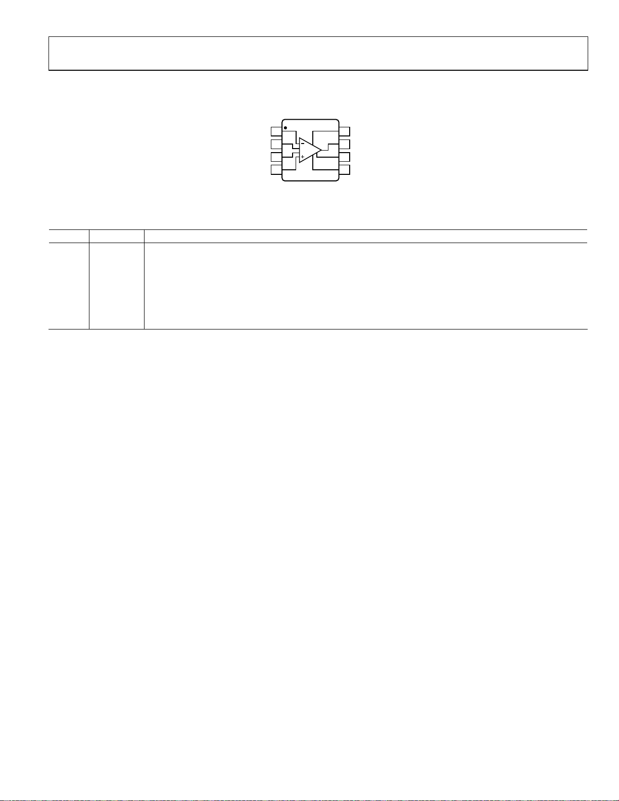
PIN CONNECTION DIAGRAM
AD8421
1
–IN
2
R
G
3
R
G
4
+IN
TOP VIEW
(Not to Scale)
Figure 1.
10µ
G = 100
1µ
100n
8
+V
S
7
V
OUT
6
REF
5
–V
S
10123-001
BEST AVAILABLE
7mA LOW NOISE IN-AMP
APPLICATIONS
Medical instrumentation
Precision data acquisition
Microphone preamplification
Vibration analysis
Multiplexed input applications
ADC driver
GENERAL DESCRIPTION
The AD8421 is a low cost, low power, extremely low noise, ultralow
bias current, high speed instrumentation amplifier that is ideally
suited for a broad spectrum of signal conditioning and data
acquisition applications. This product features extremely high
CMRR, allowing it to extract low level signals in the presence of
high frequency common-mode noise over a wide temperature
range.
The 10 MHz bandwidth, 35 V/µs slew rate, and 0.6 µs settling
time to 0.001% (G = 10) allow the AD8421 to amplify high speed
signals and excel in applications that require high channel count,
multiplexed systems. Even at higher gains, the current feedback
architecture maintains high performance; for example, at G = 100,
the bandwidth is 2 MHz and the settling time is 0.8 µs. The
AD8421 has excellent distortion performance, making it suitable
for use in demanding applications such as vibration analysis.
Rev. 0
Information furnished by Analog Devices is believed to be accurate and reliable. However, no
responsibility is assumed by Anal og Devices for its use, nor for any infringements of patents or ot her
rights of third parties that may result from its use. Specifications subject to change without notice. No
license is granted by implication or otherwise under any patent or patent rights of Analog Devices.
Trademarks and registered trademarks are the property of their respective owners.
BEST AVAILABLE
1mA LOW POWER IN-AMP
10n
AD8421
TOTAL NOISE DENSITY AT 1kHz (V/√Hz)
1n
100 1M
Figure 2. Noise Density vs. Source Resistance
R
NOISE ONLY
S
1k 10k 100k
SOURCE RESISTANCE, RS (Ω)
The AD8421 delivers 3 nV/√Hz input voltage noise and
200 fA/√Hz current noise with only 2 mA quiescent current,
making it an ideal choice for measuring low level signals. For
applications with high source impedance, the AD8421 employs
innovative process technology and design techniques to provide
noise performance that is limited only by the sensor.
The AD8421 uses unique protection methods to ensure robust
inputs while still maintaining very low noise. This protection
allows input voltages up to 40 V from the opposite supply rail
without damage to the part.
A single resistor sets the gain from 1 to 10,000. The reference
pin can be used to apply a precise offset to the output voltage.
The AD8421 is specified from −40°C to +85°C and has typical
performance curves to 125°C. It is available in 8-lead MSOP
and SOIC packages.
One Technology Way, P.O. Box 9106, Norwood, MA 02062-9106, U.S.A.
Tel: 781.329.4700 www.analog.com
Fax: 781.461.3113 ©2012 Analog Devices, Inc. All rights reserved.
10123-078

AD8421 Data Sheet
TABLE OF CONTENTS
Features.............................................................................................. 1
Applications....................................................................................... 1
Pin Connection Diagram ................................................................ 1
General Description......................................................................... 1
Revision History ...............................................................................2
Specifications..................................................................................... 3
AR and BR Grades........................................................................ 3
ARM and BRM Grades................................................................ 5
Absolute Maximum Ratings............................................................ 8
Thermal Resistance...................................................................... 8
ESD Caution.................................................................................. 8
Pin Configuration and Function Descriptions............................. 9
Typical Performance Characteristics........................................... 10
Theory of Operation ......................................................................20
Architecture................................................................................. 20
Gain Selection............................................................................. 20
Reference Terminal.................................................................... 21
Input Voltage Range................................................................... 21
Layout .......................................................................................... 21
Input Bias Current Return Path ............................................... 22
Input Voltages Beyond the Supply Rails.................................. 22
Radio Frequency Interference (RFI)........................................ 23
Calculating the Noise of the Input Stage................................. 23
Applications Information.............................................................. 25
Differential Output Configuration .......................................... 25
Driving an ADC ......................................................................... 26
Outline Dimensions....................................................................... 27
Ordering Guide .......................................................................... 27
REVISION HISTORY
5/12—Revision 0: Initial Version
Rev. 0 | Page 2 of 28

Data Sheet AD8421
SPECIFICATIONS
VS = ±15 V, V
AR AND BR GRADES
Table 1.
Parameter
COMMON-MODE REJECTION
RATIO (CMRR)
CMRR DC to 60 Hz with 1 kΩ
Source Imbalance
G = 1 86 94 dB
G = 10 106 114 dB
G = 100 126 134 dB
G = 1000 136 140 dB
Over Temperature, G = 1 T = −40°C to +85°C 80 93 dB
CMRR at 20 kHz VCM = −10 V to +10 V
G = 1 80 80 dB
G = 10 90 100 dB
G = 100 100 110 dB
G = 1000 110 120 dB
NOISE
Voltage Noise, 1 kHz1 V
Input Voltage Noise, eni 3 3.2 3 3.2 nV/√Hz
Output Voltage Noise, eno 60 60 nV/√Hz
Peak to Peak, RTI f = 0.1 Hz to 10 Hz
G = 1 2 2 2.2 μV p-p
G = 10 0.5 0.5 μV p-p
G = 100 to 1000 0.07 0.07 0.09 μV p-p
Current Noise
Spectral Density f = 1 kHz 200 200 fA/√Hz
Peak to Peak, RTI f = 0.1 Hz to 10 Hz 18 18 pA p-p
VOLTAGE OFFSET2
Input Offset Voltage, V
Over Temperature TA = −40°C to +85°C 86 45 μV
Average TC 0.4 0.2 μV/°C
Output Offset Voltage, V
Over Temperature TA = −40°C to +85°C 0.66 0.45 mV
Average TC 6 5 μV/°C
Offset RTI vs. Supply (PSR) VS = ±2.5 V to ±18 V
G = 1 90 120 100 120 dB
G = 10 110 120 120 140 dB
G = 100 124 130 140 150 dB
G = 1000 130 140 140 150 dB
INPUT CURRENT
Input Bias Current 1 2 0.1 0.5 nA
Over Temperature TA = −40°C to +85°C 8 6 nA
Average TC 50 50 pA/°C
Input Offset Current 0.5 2 0.1 0.5 nA
Over Temperature TA = −40°C to +85°C 2.2 0.8 nA
Average TC 1 1 pA/°C
= 0 V, TA = 25°C, G = 1, RL = 2 k, unless otherwise noted.
REF
Test Conditions/
Comments
Min Typ Max Min Typ Max
V
= −10 V to +10 V
CM
+, VIN− = 0 V
IN
V
OSI
350 250 μV
OSO
= ±5 V to ±15 V 60 25 μV
S
AR Grade BR Grade
Unit
Rev. 0 | Page 3 of 28

AD8421 Data Sheet
Test Conditions/
Parameter
Comments
Min Typ Max Min Typ Max
DYNAMIC RESPONSE
Small Signal Bandwidth −3 dB
G = 1 10 10 MHz
G = 10 10 10 MHz
G = 100 2 2 MHz
G = 1000 0.2 0.2 MHz
Settling Time to 0.01% 10 V step
G = 1 0.7 0.7 μs
G = 10 0.4 0.4 μs
G = 100 0.6 0.6 μs
G = 1000 5 5 μs
Settling Time to 0.001% 10 V step
G = 1 1 1 μs
G = 10 0.6 0.6 μs
G = 100 0.8 0.8 μs
G = 1000 6 6 μs
Slew Rate
G = 1 to 100 35 35 V/μs
GAIN3 G = 1 + (9.9 kΩ/RG)
Gain Range 1 10,000 1 10,000 V/V
Gain Error V
= ±10 V
OUT
G = 1 0.02 0.01 %
G = 10 to 1000 0.2 0.1 %
Gain Nonlinearity V
= −10 V to +10 V
OUT
G = 1 RL ≥ 2 kΩ 1 1 ppm
R
= 600 Ω 1 3 1 3 ppm
L
G = 10 to 1000 RL ≥ 600 Ω 30 50 30 50 ppm
V
= −5 V to +5 V 5 10 5 10 ppm
OUT
Gain vs. Temperature3
G = 1 5 0.1 1 ppm/°C
G > 1 −50 −50 ppm/°C
INPUT
Input Impedance
Differential 30||3 30||3 GΩ||pF
Common Mode 30||3 30||3 GΩ||pF
Input Operating Voltage Range4 VS = ±2.5 V to ±18 V −VS + 2.3 +VS − 1.8 −VS + 2.3 +VS − 1.8 V
Over Temperature TA = −40°C −VS + 2.5 +VS − 2.0 −VS + 2.5 +VS − 2.0 V
T
= +85°C −VS + 2.1 +VS − 1.8 −VS + 2.1 +VS − 1.8 V
A
OUTPUT RL = 2 kΩ
Output Swing VS = ±2.5 V to ±18 V −VS + 1.2 +Vs − 1.6 −VS + 1.2 +VS − 1.6 V
Over Temperature TA = −40°C to +85°C −VS + 1.2 +Vs − 1.6 −VS + 1.2 +VS − 1.6 V
Short-Circuit Current 65 65 mA
REFERENCE INPUT
RIN 20 20 kΩ
IIN V
+, VIN− = 0 V 20 24 20 24 μA
IN
Voltage Range −VS +VS −VS +VS V
Reference Gain to Output
AR Grade BR Grade
1 ±
0.0001
1 ±
0.0001
Unit
V/V
Rev. 0 | Page 4 of 28

Data Sheet AD8421
Test Conditions/
Parameter
Comments
Min Typ Max Min Typ Max
POWER SUPPLY
Operating Range Dual supply ±2.5 ±18 ±2.5 ±18 V
Single supply 5 36 5 36 V
Quiescent Current 2 2.3 2 2.3 mA
Over Temperature TA = −40°C to +85°C 2.6 2.6 mA
TEMPERATURE RANGE
For Specified Performance −40 +85 −40 +85 °C
Operational5 −40 +125 −40 +125 °C
1
Total voltage noise = √(e
2
Total RTI VOS = (V
3
These specifications do not include the tolerance of the external gain setting resistor, RG. For G > 1, add RG errors to the specifications given in this table.
4
Input voltage range of the AD8421 input stage only. The input range can depend on the common-mode voltage, differential voltage, gain, and reference voltage.
See the section for more details. Input Voltage Range
5
See the section for expected operation between 85°C and 125°C. Typical Performance Characteristics
OSI
) + (V
2
+ (eno/G)2 + e
ni
/G).
OSO
2
). See the Th section for more information. eory of Operation
RG
ARM AND BRM GRADES
Table 2.
Test Conditions/
Parameter
COMMON-MODE REJECTION
RATIO (CMRR)
CMRR DC to 60 Hz with 1 kΩ
Source Imbalance
G = 1 84 92 dB
G = 10 104 112 dB
G = 100 124 132 dB
G = 1000 134 140 dB
Over Temperature, G = 1 TA = −40°C to +85°C 80 90 dB
CMRR at 20 kHz VCM = −10 V to +10 V
G = 1 80 80 dB
G = 10 90 90 dB
G = 100 100 100 dB
G = 1000 100 100 dB
NOISE
Voltage Noise, 1 kHz1 V
Input Voltage Noise, eni 3 3.2 3 3.2 nV/√Hz
Output Voltage Noise, eno 60 60 nV/√Hz
Peak to Peak, RTI f = 0.1 Hz to 10 Hz
G = 1 2 2 2.2 μV p-p
G = 10 0.5 0.5 μV p-p
G = 100 to 1000 0.07 0.07 0.09 μV p-p
Current Noise
Spectral Density f = 1 kHz 200 200 fA/√Hz
Peak to Peak, RTI f = 0.1 Hz to 10 Hz 18 18 pA p-p
VOLTAGE OFFSET2
Input Offset Voltage, V
V
OSI
Over Temperature TA = −40°C to +85°C 135 135 μV
Average TC 0.9 0.9 μV/°C
Output Offset Voltage, V
OSO
Over Temperature TA = −40°C to +85°C 1 1 mV
Average TC 9 9 μV/°C
Comments
Min Typ Max Min Typ Max
= −10 V to +10 V
V
CM
+, VIN− = 0 V
IN
= ±5 V to ±15 V 70 50 μV
S
600 400 μV
AR Grade BR Grade
Unit
ARM Grade BRM Grade
Unit
Rev. 0 | Page 5 of 28

AD8421 Data Sheet
Test Conditions/
Parameter
Comments
Min Typ Max Min Typ Max
Offset RTI vs. Supply (PSR) VS = ±2.5 V to ±18 V
G = 1 90 120 100 120 dB
G = 10 110 120 120 140 dB
G = 100 124 130 140 150 dB
G = 1000 130 140 140 150 dB
INPUT CURRENT
Input Bias Current 1 2 0.1 1 nA
Over Temperature TA = −40°C to +85°C 8 6 nA
Average TC 50 50 pA/°C
Input Offset Current 0.5 2 0.1 1 nA
Over Temperature TA = −40°C to +85°C 3 1.5 nA
Average TC 1 1 pA/°C
DYNAMIC RESPONSE
Small Signal Bandwidth −3 dB
G = 1 10 10 MHz
G = 10 10 10 MHz
G = 100 2 2 MHz
G = 1000 0.2 0.2 MHz
Settling Time 0.01% 10 V step
G = 1 0.7 0.7 μs
G = 10 0.4 0.4 μs
G = 100 0.6 0.6 μs
G = 1000 5 5 μs
Settling Time 0.001% 10 V step
G = 1 1 1 μs
G = 10 0.6 0.6 μs
G = 100 0.8 0.8 μs
G = 1000 6 6 μs
Slew Rate
G = 1 to 100 35 35 V/μs
GAIN3 G = 1 + (9.9 kΩ/RG)
Gain Range 1 10,000 1 10,000 V/V
Gain Error V
= ±10 V
OUT
G = 1 0.05 0.02 %
G = 10 to 1000 0.3 0.2 %
Gain Nonlinearity V
= −10 V to +10 V
OUT
G = 1 RL ≥ 2 kΩ 1 1 ppm
R
= 600 Ω 1 3 1 3 ppm
L
G = 10 to 1000 RL ≥ 600 Ω 30 50 30 50 ppm
V
= −5 V to +5 V 5 10 5 10 ppm
OUT
Gain vs. Temperature3
G = 1 5 0.1 1 ppm/°C
G > 1 −50 −50 ppm/°C
INPUT
Input Impedance
Differential 30||3 30||3 GΩ||pF
Common Mode 30||3 30||3 GΩ||pF
Input Operating Voltage
Range
4
VS = ±2.5 V to ±18 V −VS + 2.3 +VS − 1.8 −VS + 2.3 +VS − 1.8 V
Over Temperature TA = −40°C −VS + 2.5 +VS − 2.0 −VS + 2.5 +VS − 2.0 V
T
= +85°C −VS + 2.1 +VS − 1.8 −VS + 2.1 +VS − 1.8 V
A
ARM Grade BRM Grade
Unit
Rev. 0 | Page 6 of 28

Data Sheet AD8421
Test Conditions/
Parameter
Comments
Min Typ Max Min Typ Max
OUTPUT RL = 2 kΩ
Output Swing VS = ±2.5 V to ±18 V −VS + 1.2 +VS − 1.6 −VS + 1.2 +Vs − 1.6 V
Over Temperature TA = −40°C to +85°C −VS + 1.2 +VS − 1.6 −VS + 1.2 +Vs − 1.6 V
Short-Circuit Current 65 65 mA
REFERENCE INPUT
RIN 20 20 kΩ
IIN V
+, VIN− = 0 V 20 24 20 24 μA
IN
Voltage Range −VS +VS −VS +VS V
Reference Gain to Output
POWER SUPPLY
Operating Range Dual supply ±2.5 ±18 ±2.5 ±18 V
Single supply 5 36 5 36 V
Quiescent Current 2 2.3 2 2.3 mA
Over Temperature TA = −40°C to +85°C 2.6 2.6 mA
TEMPERATURE RANGE
For Specified Performance −40 +85 −40 +85 °C
Operational5 −40 +125 −40 +125 °C
1
Total voltage noise = √(e
2
Total RTI VOS = (V
3
These specifications do not include the tolerance of the external gain setting resistor, RG. For G > 1, add RG errors to the specifications given in this table.
4
Input voltage range of the AD8421 input stage only. The input range can depend on the common-mode voltage, differential voltage, gain, and reference voltage.
See the section for more information. Input Voltage Range
5
See the section for expected operation between 85°C and 125°C. Typical Performance Characteristics
OSI
) + (V
2
+ (eno/G)2 + e
ni
/G).
OSO
2
). See the Th section for more information. eory of Operation
RG
ARM Grade BRM Grade
1 ±
0.0001
1 ±
0.0001
Unit
V/V
Rev. 0 | Page 7 of 28
AD8421 Data Sheet
ABSOLUTE MAXIMUM RATINGS
Table 3.
Parameter Rating
Supply Voltage ±18 V
Output Short-Circuit Current Duration Indefinite
Maximum Voltage at −IN or +IN1 −VS + 40 V
Minimum Voltage at −IN or +IN +VS − 40 V
Maximum Voltage at REF2 +VS + 0.3 V
Minimum Voltage at REF −VS − 0.3 V
Storage Temperature Range −65°C to +150°C
Operating Temperature Range −40°C to +125°C
Maximum Junction Temperature 150°C
ESD
Human Body Model 2 kV
Charged Device Model 1.25 kV
Machine Model 0.2 kV
1
For voltages beyond these limits, use input protection resistors. See the
Theory of Operation section for more information.
2
There are ESD protection diodes from the reference input to each supply, so
REF cannot be driven beyond the supplies in the same way that +IN and −IN
can. See the Reference Terminal section for more information.
Stresses above those listed under Absolute Maximum Ratings
may cause permanent damage to the device. This is a stress
rating only; functional operation of the device at these or any
other conditions above those indicated in the operational
section of this specification is not implied. Exposure to absolute
maximum rating conditions for extended periods may affect
device reliability.
THERMAL RESISTANCE
θJA is specified for a device in free air using a 4-layer JEDEC
printed circuit board (PCB).
Table 4.
Package θJA Unit
8-Lead SOIC 107.8 °C/W
8-Lead MSOP 138.6 °C/W
ESD CAUTION
Rev. 0 | Page 8 of 28
Data Sheet AD8421
PIN CONFIGURATION AND FUNCTION DESCRIPTIONS
–IN
R
R
+IN
G
G
1
2
3
4
(Not to Scale)
AD8421
TOP VIEW
8
+V
S
7
V
OUT
6
REF
5
–V
S
10123-002
Figure 3. Pin Configuration
Table 5. Pin Function Descriptions
Pin No. Mnemonic Description
1 −IN Negative Input Terminal.
2, 3 RG Gain Setting Terminals. Place resistor across the RG pins to set the gain. G = 1 + (9.9 kΩ/RG).
4 +IN Positive Input Terminal.
5 −VS Negative Power Supply Terminal.
6 REF Reference Voltage Terminal. Drive this terminal with a low impedance voltage source to level shift the output.
7 V
Output Terminal.
OUT
8 +VS Positive Power Supply Terminal.
Rev. 0 | Page 9 of 28

AD8421 Data Sheet
TYPICAL PERFORMANCE CHARACTERISTICS
TA = 25°C, VS = ±15 V, V
600
= 0 V, RL = 2 kΩ, unless otherwise noted.
REF
600
500
400
300
UNITS
200
100
0
–60 –40 –20 20 4006
INPUT OFFSET VOLTAGE (µV)
0
10123-003
Figure 4. Typical Distribution of Input Offset Voltage
1800
1500
1200
900
UNITS
600
500
400
300
UNITS
200
100
0
–400 –300 300200–200 –100 0 100 400
OUTPUT OFFSET VOLTAGE (µV)
Figure 7. Typical Distribution of Output Offset Voltage
1200
1000
800
600
UNITS
400
10123-006
300
0
–2.0 –1.5 1.51.0–1.0 –0.5 0 0.5 2.0
INPUT BIAS CURRENT (nA)
Figure 5. Typical Distribution of Input Bias Current
1400
1200
1000
800
UNITS
600
400
200
0
–20 –15 1510–10 –5 0 5 20
PSRR (µV/V)
Figure 6. Typical Distribution of PSRR (G = 1)
200
0
10123-004
–2.0 –1.5 –1. 0 –0.5 0.5 1.0 1.502
INPUT O FFSET CURRENT (n A)
.0
10123-007
Figure 8. Typical Distribution of Input Offset Current
1600
1400
1200
1000
800
UNITS
600
400
200
0
10123-005
–120 1209060300–30–60–90
CMRR (µV/V)
10123-008
Figure 9. Typical Distribution of CMRR (G = 1)
Rev. 0 | Page 10 of 28

Data Sheet AD8421
15
G = 1
10
5
0
–5
COMMON-MO DE VOLT AGE (V)
–10
VS = ±12V
VS = ±15V
4
G = 100
3
2
1
0
–1
COMMON-MODE VOLTAGE (V)
–2
VS = ±5V
VS = ±2.5V
–15
–15 15105–5–10 0
OUTPUT VOLTAGE (V)
Figure 10. Input Common-Mode Voltage vs. Output Voltage;
= ±12 V and ±15 V (G = 1)
V
S
4
G = 1
3
2
1
0
–1
COMMON-MODE VOLTAGE (V)
–2
–3
–4 4321–3 –2 –1 0
OUTPUT VOLTAGE (V)
VS = ±5V
VS = ±2.5V
Figure 11. Input Common-Mode Voltage vs. Output Voltage;
= ±2.5 V and ±5 V (G = 1)
V
S
15
G = 100
10
5
VS = ±12V
VS = ±15V
–3
–4 4321–3 –2 –1 0
10123-009
OUTPUT VOLTAGE (V)
10123-012
Figure 13. Input Common-Mode Voltage vs. Output Voltage;
V
= ±2.5 V and ±5 V (G = 100)
S
40
VS = 5V
G = 1
30
20
10
0
–10
INPUT CURRENT (mA)
–20
–30
–40
–30–25–20–15–10–5 0 5 101520253035
10123-010
–35 40
Figure 14. Input Overvoltage Performance; G = 1, +V
30
VS = ±15V
G = 1
20
10
INPUT VOLTAGE (V)
= 5 V, −VS = 0 V
S
10123-013
0
–5
COMMON-MO DE VOLT AGE (V)
–10
–15
–15 15105–5–10 0
OUTPUT VOLTAGE (V)
Figure 12. Input Common-Mode Voltage vs. Output Voltage;
= ±12 V and ±15 V (G = 100)
V
S
10123-011
Rev. 0 | Page 11 of 28
0
–10
INPUT CURRENT (mA)
–20
–30
–25 25
–20 –15 –10 –5 0 5 10 15 20
INPUT VOLTAGE (V)
Figure 15. Input Overvoltage Performance; G = 1, V
= ±15 V
S
10123-014

AD8421 Data Sheet
40
VS = 5V
G = 100
30
20
10
0
–10
INPUT CURRENT (mA)
–20
–30
160
140
120
100
80
60
POSITIVE PSRR (dB)
40
20
GAIN = 1000
GAIN = 100
GAIN = 10
GAIN = 1
–40
–30–25–20–15–10–5 0 5 101520253035
–35 40
Figure 16. Input Overvoltage Performance; +V
30
VS = ±15V
G = 100
20
10
0
–10
INPUT CURRENT (mA)
–20
–30
–25 25
–20 –15 –10 –5 0 5 10 15 20
INPUT VOLTAGE (V)
INPUT VOLTAGE (V)
= 5 V, −VS = 0 V, G = 100
S
Figure 17. Input Overvoltage Performance; V
2.5
2.0
1.5
1.0
0.5
0
–0.5
BIAS CURRENT (nA)
–1.0
–1.5
–2.0
–2.5
–12 14
–10–8–6–4–2024681012
COMMON-MODE VOLTAGE (V)
Figure 18. Input Bias Current vs. Common-Mode Voltage
= ±15 V, G = 100
S
0
0.1 1 10 100 1k 10k 100k 1M
10123-015
FREQUENCY (Hz)
10123-018
Figure 19. Positive PSRR vs. Frequency
160
GAIN = 1000
GAIN = 100
140
GAIN = 10
120
GAIN = 1
100
80
60
NEGATIVE PSRR (dB)
40
20
0
0.1 1 10 100 1k 10k 100k 1M
10123-016
FREQUENCY (Hz)
10123-019
Figure 20. Negative PSRR vs. Frequency
70
GAIN = 1000
60
50
GAIN = 100
40
30
GAIN = 10
20
GAIN (dB)
10
GAIN = 1
0
–10
–20
–30
10123-017
100 1k 10k 100k 1M 10M
FREQUENCY (Hz)
10123-020
Figure 21. Gain vs. Frequency
Rev. 0 | Page 12 of 28

Data Sheet AD8421
160
140
120
100
CMRR (dB)
GAIN = 1000
GAIN = 100
GAIN = 10
GAIN = 1
80
6
REPRESENTATIVE SAMPLES
4
2
0
–2
BIAS CURRENT (nA)
–4
60
40
0.1 1 10 100 1k 10k 100k
FREQUENCY (Hz)
Figure 22. CMRR vs. Frequency
160
GAIN = 1000
140
GAIN = 100
120
GAIN = 10
100
GAIN = 1
CMRR (dB)
80
60
40
0.1 1 10 100 1k 10k 100k
FREQUENCY (Hz)
Figure 23. CMRR vs. Frequency, 1 kΩ Source Imbalance
–6
–8
–40 125
–25–105 203550658095110
10123-021
TEMPERATURE (°C)
10123-024
Figure 25. Input Bias Current vs. Temperature
100
REPRESENTATIVE SAMPLES
GAIN = 1
80
60
40
20
0
–20
GAIN ERROR (µV/V)
–40
–60
–80
–25–105 203550658095110
–40 125
10123-022
TEMPERATURE (°C)
10123-025
Figure 26. Gain vs. Temperature (G = 1)
2.0
1.5
1.0
0.5
0
CHANGE IN INP UT OFF SET VOLTAGE ( µV)
–0.5
05
5 1015202530354045 0
Figure 24. Change in Input Offset Voltage (V
WARM-UP TIME (Seconds)
OSI
) vs. Warm-Up Time
10123-023
15
REPRESENTATIVE SAMPLES
GAIN = 1
10
5
0
CMRR (µV/V)
–5
–10
–15
–25–105 203550658095110
–40 125
Figure 27. CMRR vs. Temperature (G = 1)
Rev. 0 | Page 13 of 28
TEMPERATURE (°C)
10123-074

AD8421 Data Sheet
V
V
3.0
2.5
2.0
VS = ±15V
VS = ±5V
40
–SR
35
30
25
+SR
1.5
1.0
SUPPLY CU RRENT (mA)
0.5
0
–40 125
–25 –10 5 20 35 50 65 80 95 110
TEMPERATURE (°C)
Figure 28. Supply Current vs. Temperature (G = 1)
80
60
I
40
20
0
–20
–40
–60
–80
SHORT- CIRCUIT CURRENT (mA)
–100
–120
–40 110
–25 –10 5 20 35 50 65 80 95 125
SHORT+
I
SHORT–
TEMPERATURE (°C)
Figure 29. Short-Circuit Current vs. Temperature (G = 1)
20
15
SLEW RATE (V/µs)
10
5
0
–40 125
–25 –10 5 20 35 50 65 80 95 110
10123-026
Figure 31. Slew Rate vs. Temperature, V
+
S
–0.5
–1.0
–1.5
–2.0
–2.5
+2.5
+2.0
INPUT VOLTAGE (V)
+1.5
+1.0
REFERRED TO SUPPLY VOLTAGES
+0.5
–V
S
21
4 6 8 10121416
10123-027
TEMPERATURE (°C)
SUPPLY VOLTAGE (±VS)
= ±5 V (G = 1)
S
10123-029
–40°C
+25°C
+85°C
+105°C
+125°C
8
10123-030
Figure 32. Input Voltage Limit vs. Supply Voltage
40
35
–SR
30
25
20
15
SLEW RATE (V/µs)
10
+SR
5
0
–40 125
–25 –10 5 20 35 50 65 80 95 110
Figure 30. Slew Rate vs. Temperature, V
TEMPERATURE (°C)
= ±15 V (G = 1)
S
10123-028
Rev. 0 | Page 14 of 28
+
S
–0.5
–1.0
–1.5
–2.0
–2.5
+2.5
+2.0
OUTPUT VOLTAGE (V)
+1.5
+1.0
REFERRED TO SUPPLY VOLTAGES
+0.5
–V
S
02 2018
4 6 8 10 12 14 16
SUPPLY VOLTAGE (±VS)
Figure 33. Output Voltage Swing vs. Supply Voltage, R
–40°C
+25°C
+85°C
+105°C
+125°C
= 10 kΩ
L
10123-031

Data Sheet AD8421
V
V
+
S
–0.5
–1.0
–1.5
–2.0
–2.5
+2.5
+2.0
OUTPUT VOLTAGE (V)
+1.5
+1.0
REFERRED TO SUPPLY VOLTAGES
+0.5
–V
S
02 2018
4 6 8 10 12 14 16
SUPPLY VOLTAGE (±VS)
Figure 34. Output Voltage Swing vs. Supply Voltage, R
–40°C
+25°C
+85°C
+105°C
+125°C
= 600 Ω
L
10123-032
5
4
3
2
1
0
–1
–2
NONLINEARI TY (pp m)
–3
–4
–5
–10 –8 –6 –4 –2 0 2 4 6 8 10
Figure 37. Gain Nonlinearity (G = 1), R
OUTPUT VOLTAGE (V)
= 10 kΩ, 2 kΩ
L
GAIN = 1
RL = 2kΩ
= 10kΩ
R
L
10123-035
15
10
5
0
–5
OUTPUT VOLTAGE SWING (V)
–10
–15
100 100k
1k 10k
LOAD (Ω)
Figure 35. Output Voltage Swing vs. Load Resistance
+
S
–2
–4
–6
–8
+8
+6
OUTPUT VOLTAGE SWING (V)
+4
REFERRED TO SUPPLY VOLTAGES
+2
–V
S
0 0.01 0.100.09
0.02 0.03 0. 04 0. 05 0.06 0. 07 0.08
OUTPUT CURRENT (A)
Figure 36. Output Voltage Swing vs. Output Current
–40°C
+25°C
+85°C
+105°C
+125°C
–40°C
+25°C
+85°C
+105°C
+125°C
5
4
3
2
1
0
–1
–2
NONLINEARI TY (pp m)
–3
–4
–5
–10 –8 –6 –4 –2 0 2 4 6 8 10
10123-033
RL = 600Ω
OUTPUT VOLTAGE (V)
Figure 38. Gain Nonlinearity (G = 1), R
100
80
60
40
20
0
–20
–40
NONLINEARI TY (pp m)
–60
–80
–100
–10 –8 –6 –4 –2 0 2 4 6 8 10
10123-034
Figure 39. Gain Nonlinearity (G = 1000), R
RL = 600Ω
OUTPUT VOLTAGE (V)
L
= 600 Ω, V
= 600 Ω
L
GAIN = 1000
GAIN = 1
= ±10 V
OUT
10123-036
10123-072
Rev. 0 | Page 15 of 28

AD8421 Data Sheet
100
80
60
40
20
0
–20
–40
NONLI NEARIT Y (pp m)
–60
–80
–100
–5–4–3–2–1012345
RL = 600Ω
OUTPUT VOLTAGE (V)
Figure 40. Gain Nonlinearity (G = 1000), R
1k
= 600 Ω, V
L
GAIN = 1000
OUT
= ±5 V
10123-073
10k
1k
100
CURRENT NOI SE (fA/√Hz)
10
0.1 1 10 100 1k 10k 100k
FREQUENCY (Hz)
Figure 43. Current Noise Spectral Density vs. Frequency
10123-039
100
10
VOLTAGE NOISE SPECTRAL DENSITY (nV/√Hz)
1
1 10 100 1k 10k 100k
FREQUENCY (Hz)
GAIN = 1
GAIN = 10
GAIN = 100
GAIN = 1000
Figure 41. RTI Voltage Noise Spectral Density vs. Frequency
G = 1000, 40nV/DIV
G = 1, 1µV/DIV
1s/DIV
Figure 42. 0.1 Hz to 10 Hz RTI Voltage Noise (G = 1, G = 1000)
1s/DIV5pA/DIV
10123-037
10123-040
Figure 44. 0.1 Hz to 10 Hz Current Noise
30
25
20
15
10
OUTPUT VOLTAGE (V p-p)
5
10123-038
0
10 100 1k 10k 100k 1M 10M
FREQUENCY (Hz)
10123-045
Figure 45. Large Signal Frequency Response
Rev. 0 | Page 16 of 28

Data Sheet AD8421
5V/DIV
720ns TO 0.01%
1.12µs TO 0.001%
0.002%/DIV
1µs/DIV
10123-041
Figure 46. Large Signal Pulse Response and Settling Time (G = 1),
10 V Step, V
5V/DIV
0.002%/DIV
= ±15 V, RL = 2 kΩ, CL = 100 pF
S
420ns TO 0.01%
604ns TO 0.001%
1µs/DIV
10123-042
Figure 47. Large Signal Pulse Response and Settling Time (G = 10),
10 V Step, V
= ±15 V, RL = 2 kΩ, CL = 100 pF
S
5V/DIV
3.8µs TO 0.01%
5.76µs TO 0.001%
0.002%/DIV
4µs/DIV
10123-044
Figure 49. Large Signal Pulse Response and Settling Time (G = 1000),
10 V Step, V
2500
2000
1500
SETTLED TO 0.001%
1000
SETTLING TIME (ns)
500
0
4 6 8 10 12 14 16 18 0
22
Figure 50. Settling Time vs. Step Size (G = 1), R
= ±15 V, RL = 2 kΩ, CL = 100 pF
S
SETTLED TO 0.01%
STEP SIZE (V)
= 2 kΩ, CL = 100 pF
L
GAIN = 1
10123-054
5V/DIV
704ns TO 0.01%
764ns TO 0.001%
0.002%/DIV
1µs/DIV
10123-043
Figure 48. Large Signal Pulse Response and Settling Time (G = 100),
10 V Step, V
= ±15 V, RL = 2 kΩ, CL = 100 pF
S
Rev. 0 | Page 17 of 28
GAIN = 1
50mV/DIV
Figure 51. Small Signal Pulse Response (G = 1), R
1µs/DIV
= 600 Ω, CL = 100 pF
L
10123-046

AD8421 Data Sheet
–
–
GAIN = 10
NO LOAD
20pF
50pF
100pF
G = 1
50mV/DIV
Figure 52. Small Signal Pulse Response (G = 10), R
GAIN = 100
20mV/DIV
1µs/DIV
= 600 Ω, CL = 100 pF
L
1µs/DIV
10123-047
10123-048
Figure 53. Small Signal Pulse Response (G = 100), RL = 600 Ω, CL = 100 pF
GAIN = 1000
20mV/DIV
Figure 54. Small Signal Pulse Response (G = 1000), R
2µs/DIV
= 600 Ω, CL = 100 pF
L
10123-049
50mV/DIV 1µs/DIV
10123-053
Figure 55. Small Signal Response with Various Capacitive Loads (G = 1),
= Infinity
R
L
40
RL ≥ 600Ω
–50
–60
–70
–80
–90
–100
–110
AMPLITUDE (d Bc)
–120
–130
–140
–150
10 10k1k100
FREQUENCY (Hz)
V
OUT
= 10V p-p
10123-055
Figure 56. Second Harmonic Distortion vs. Frequency (G = 1)
40
–50
–60
–70
–80
–90
–100
–110
AMPLIT UDE (dBc)
–120
–130
–140
–150
10 10k1k100
NO LOAD
= 2kΩ
R
L
= 600Ω
R
L
FREQUENCY (Hz)
V
OUT
= 10V p-p
Figure 57. Third Harmonic Distortion vs. Frequency (G = 1)
10123-056
Rev. 0 | Page 18 of 28

Data Sheet AD8421
–
–
–
40
NO LOAD
R
–50
R
–60
–70
–80
–90
AMPLITUDE (d Bc)
–100
–110
–120
10 10k1k100
= 2kΩ
L
= 600Ω
L
FREQUENCY (Hz)
V
OUT
= 10V p-p
Figure 58. Second Harmonic Distortion vs. Frequency (G = 1000)
–50
–60
–70
40
RL ≥ 600Ω
V
OUT
= 10V p-p
10123-075
20
G = 1
–30
G = 10
G = 100
–40
G = 1000
–50
–60
–70
–80
–90
–100
AMPLITUDE (d Bc)
–110
–120
–130
–140
10 10k1k100
FREQUENCY (Hz)
Figure 60. THD vs. Frequency
V
OUT
R
L
= 10V p-p
= 2kΩ
10123-077
–80
–90
AMPLITUDE (d Bc)
–100
–110
–120
10 10k1k100
FREQUENCY (Hz)
Figure 59. Third Harmonic Distortion vs. Frequency (G = 1000)
10123-076
Rev. 0 | Page 19 of 28

AD8421 Data Sheet
–
V
G
THEORY OF OPERATION
+
S
II
I
COMPENSATION
OVERVOLTAGE
IN
PROTECTION
ESD AND
B
A1 A2
C1 C2
NODE 1
R1
4.95kΩ
superβ
NODE 3 NODE 4
+V
ARCHITECTURE
The AD8421 is based on the classic 3-op-amp topology. This
topology has two stages: a preamplifier to provide differential
amplification, followed by a difference amplifier that removes the
common-mode voltage. Figure 61 shows a simplified schematic
of the AD8421.
Topologically, Q1, A1, R1 and Q2, A2, R2 can be viewed as
precision current feedback amplifiers. Input Transistors Q1 and
Q2 are biased at a fixed current so that any input signal forces
the output voltages of A1 and A2 to change accordingly. The
differential signal applied to the inputs is replicated across the
R
pins. Any current through RG also flows through R1 and R2,
G
creating a gained differential voltage between Node 1 and Node 2.
The amplified differential and common-mode signals are applied
to a difference amplifier that rejects the common-mode voltage
but preserves the amplified differential voltage. The difference
amplifier employs innovations that result in very low output errors
such as offset voltage and drift, distortion at various loads, as well
as output noise. Laser-trimmed resistors allow for a highly accurate
in-amp with gain error less than 0.01% and CMRR that exceeds
94 dB (G = 1). The high performance pinout and special attention
given to design and layout allow for high CMRR performance
across a wide frequency and temperature range.
Using superbeta input transistors and bias current compensation,
the AD8421 offers extremely high input impedance, low bias current, low offset current, low current noise, and extremely low
voltage noise of 3 nV/√Hz. The current-limiting and overvoltage
protection scheme allow the input to go 40 V from the opposite
rail at all gains without compromising the noise performance.
The transfer function of the AD8421 is
V
= G × (V
OUT
where G = 1 +
− V
) + V
+IN
−IN
kΩ9.9
R
G
REF
V
B
+V
S
R
–V
GAIN STAGE
S
G
S
Figure 61. Simplified Schematic
NODE 2
R2
4.95kΩ
I
B
Q2Q1
superβ
COMPENSATION
ESD AND
OVERVOLTAGE
PROTECTION
II
10kΩ
10kΩ
10kΩ
A3
+V
10kΩ
+IN
–V
DIFFE RENCE
AMPLIFIER ST AGE
+V
S
OUTPUT
S
–V
S
REF
S
10123-057
Users can easily and accurately set the gain using a single
standard resistor.
GAIN SELECTION
Placing a resistor across the RG terminals sets the gain of the
AD8421. The gain can be calculated by referring to Tabl e 6 or
by using the following gain equation:
R
The AD8421 defaults to G = 1 when no gain resistor is used. To
determine the total gain accuracy of the system, add the tolerance
and gain drift of the R
When the gain resistor is not used, gain error and gain drift are
minimal.
Table 6. Gains Achieved Using 1% Resistors
1% Standard Table Value of RG Calculated Gain
10 kΩ 1.99
2.49 kΩ 4.98
1.1 kΩ 10.00
523 Ω 19.93
200 Ω 50.50
100 Ω 100.0
49.9 Ω 199.4
20 Ω 496.0
10 Ω 991.0
4.99 Ω 1985
RG Power Dissipation
The AD8421 duplicates the differential voltage across its inputs
onto the R
to handle the expected power dissipation at ambient temperature.
kΩ9.9
=
G
1
−
resistor to the specifications of the AD8421.
G
resistor. Choose an RG resistor size that is sufficient
G
Rev. 0 | Page 20 of 28

Data Sheet AD8421
V
REFERENCE TERMINAL
The output voltage of the AD8421 is developed with respect to
the potential on the reference terminal. This can be used to sense
the ground at the load, thereby taking advantage of the CMRR to
reject ground noise or to introduce a precise offset to the signal
at the output. For example, a voltage source can be tied to the REF
pin to level shift the output, allowing the AD8421 to drive a singlesupply ADC. The REF pin is protected with ESD diodes and
should not exceed either +V
or −VS by more than 0.3 V.
S
For best performance, maintain a source impedance to the
REF terminal that is below 1 Ω. As shown in Figure 61, the
reference terminal, REF, is at one end of a 10 k resistor.
Additional impedance at the REF terminal adds to this 10 k
resistor and results in amplification of the signal connected to
the positive input. The amplification from the additional R
REF
can be calculated as follows:
2(10 k + R
)/(20 k + R
REF
REF
)
Only the positive signal path is amplified; the negative path is
unaffected. This uneven amplification degrades CMRR.
INCORRECT
AD8421
REF
V
Figure 62. Driving the Reference Pin
V
CORRECT
AD8421
+
OP1177
–
REF
10123-058
INPUT VOLTAGE RANGE
The 3-op-amp architecture of the AD8421 applies gain in the
first stage before removing the common-mode voltage in the
difference amplifier stage. Internal nodes between the first and
second stages (Node 1 and Node 2 in Figure 61) experience
a combination of a gained signal, a common-mode signal, and
a diode drop. The voltage supplies can limit the combined signal,
even when the individual input and output signals are not limited.
Figure 10 through Figure 13 show this limitation in detail.
LAYOUT
To ensure optimum performance of the AD8421 at the PCB level,
care must be taken in the design of the board layout. The pins of
the AD8421 are arranged in a logical manner to aid in this task.
1
–IN
2
R
G
3
R
G
4
+IN
AD8421
TOP VIEW
(Not to Scale)
Figure 63. Pin Configuration Diagram
8
+V
S
7
V
OUT
6
REF
5
–V
S
10123-059
Common-Mode Rejection Ratio over Frequency
Poor layout can cause some of the common-mode signals to
be converted to differential signals before reaching the in-amp.
Such conversions occur when one input path has a frequency
response that is different from the other. To maintain high CMRR
over frequency, closely match the input source impedance and
capacitance of each path. Place additional source resistance in
the input path (for example, input protection resistors) close to
the in-amp inputs, to minimize the interaction of the resistance
with parasitic capacitance from the PCB traces.
Parasitic capacitance at the gain setting pins (R
) can also affect
G
CMRR over frequency. If the board design has a component at
the gain setting pins (for example, a switch or jumper), choose
a component such that the parasitic capacitance is as small as
possible.
Power Supplies and Grounding
Use a stable dc voltage to power the instrumentation amplifier.
Noise on the supply pins can adversely affect performance.
Place a 0.1 µF capacitor as close as possible to each supply pin.
Because the length of the bypass capacitor leads is critical at
high frequency, surface-mount capacitors are recommended.
Any parasitic inductance in the bypass ground trace works against
the low impedance that is created by the bypass capacitor. As
shown in Figure 64, a 10 µF capacitor can be used farther away
from the device. For these larger value capacitors, which are
intended to be effective at lower frequencies, the current return
path distance is less critical. In most cases, the 10 µF capacitor
can be shared by other local precision integrated circuits.
+
S
0.1µF 10µF
+IN
V
LOAD
OUT
10123-060
R
G
AD8421
–IN
REF
0.1µF 10µF
–V
S
Figure 64. Supply Decoupling, REF, and Output Referred to Local Ground
A ground plane layer helps to reduce parasitic inductances, which
minimizes voltage drops with changes in current. The area of
the current path is directly proportional to the magnitude of
parasitic inductances and, therefore, the impedance of the path
at high frequency. Large changes in currents in an inductive
decoupling path or ground return create unwanted effects due
to the coupling of such changes into the amplifier inputs.
Because load currents flow from the supplies, the load should be
connected at the same physical location as the bypass capacitor
grounds.
Rev. 0 | Page 21 of 28

AD8421 Data Sheet
V
V
V
Reference Pin
The output voltage of the AD8421 is developed with respect to
the potential on the reference terminal. Ensure that REF is tied
to the appropriate local ground.
INPUT BIAS CURRENT RETURN PATH
The input bias current of the AD8421 must have a return path
to ground. When using a floating source without a current return
path (such as a thermocouple), create a current return path as
shown in Figure 65.
INCORRECT
+V
S
AD8421
–V
S
TRANSFORMER
+V
S
AD8421
–V
THERMOCOUPL E
S
REF
REF
10MΩ
CORRECT
+V
S
AD8421
–V
S
TRANSFORMER
+V
S
AD8421
–V
THERMOCOUPL E
S
REF
REF
protection required at all gains. For example, if +V
−V
= −8 V, the part can safely withstand voltages from −35 V to
S
+32 V.
The remaining AD8421 terminals should be kept within the
supplies. All terminals of the AD8421 are protected against ESD.
Input Voltages Beyond the Maximum Ratings
For applications where the AD8421 encounters voltages beyond the
limits in the Absolute Maximum Ratings table, external protection
is required. This external protection depends on the duration of
the overvoltage event and the noise performance that is required.
For short-lived events, transient protectors (such as metal oxide
varistors (MOVs)), may be all that is required.
+
S
+
I
V
IN+
–
+
V
IN–
–
R
PROTECT
+
V
IN+
–
R
PROTECT
+
V
IN–
–
AD8421
–V
S
+V
S
I
AD8421
–V
S
SIMPLE CONTINUOUS PROT ECTIONTRANSIENT PROTECT ION
V
V
R
+
V
IN+
–
R
+
V
IN–
–
R
PROTECT
+
IN+
–
R
PROTECT
+
IN–
–
PROTECT
PROTECT
I
+V
S
I
–V
S
+V
S
–V
S
= +5 V and
S
+
S
AD8421
–V
S
+V
S
AD8421
–V
S
+V
S
C
AD8421
C
CAPACITIVELY COUPLED
REF
–V
S
f
=
HIGH-PASS
CAPACITIVELY COUPLED
1
2πRC
C
C
+V
S
R
AD8421
REF
R
–V
S
Figure 65. Creating an Input Bias Current Return Path
INPUT VOLTAGES BEYOND THE SUPPLY RAILS
The AD8421 has very robust inputs. It typically does not need
additional input protection, as shown in Figure 66.
+
S
+
V
V
Figure 66. Typical Application; No Input Protection Required
The AD8421 inputs are current limited; therefore, input voltages
can be up to 40 V from the opposite supply rail, with no input
I
IN+
–
+
IN+
–
MOST APPLICATIONS
AD8421
–V
S
10123-062
LOW NO ISE CONT INUOUS
OPTION 1
LOW NO ISE CONT INUOUS
OPTION 2
10123-063
Figure 67. Input Protection Options for Input Voltages Beyond Absolute
Maximum Ratings
For longer events, use resistors in series with the inputs, combined
with diodes. To avoid degrading bias current performance, low
leakage diodes such as the BAV199 or FJH1100 are recommended.
The diodes prevent the voltage at the input of the amplifier from
10123-061
exceeding the maximum ratings, and the resistors limit the current
into the diodes. Because most external diodes can easily handle
100 mA or more, resistor values do not need to be large and,
therefore, have a minimal impact on noise performance.
At the expense of some noise performance, another solution is
to use series resistors. In the case of overvoltage, current into
the AD8421 inputs is internally limited. Although the AD8421
inputs must be kept within the limits defined in the Absolute
Maximum Ratings section, the I × R drop across the protection
resistor increases the maximum voltage that the system can
withstand, as follows:
For positive input signals
V
= (40 V + Negative Supply) + IIN × R
MAX_NEW
PROTECT
For negative input signals
V
= (Positive Supply − 40 V) − I
MIN_NEW
OUT
× R
PROTECT
Rev. 0 | Page 22 of 28

Data Sheet AD8421
V
R
()(
Overvoltage performance is shown in Figure 14, Figure 15,
Figure 16, and Figure 17. The AD8421 inputs can withstand
a current of 40 mA at room temperature for at least a day. This
time is cumulative over the life of the device. If long periods of
overvoltage are expected, the use of an external protection method
is recommended. Under extreme input conditions, the output
of the amplifier may invert.
RADIO FREQUENCY INTERFERENCE (RFI)
RF rectification is often a problem when amplifiers are used in
applications that have strong RF signals. The problem is intensified
if long leads or PCB traces are required to connect the amplifier
to the signal source. The disturbance can appear as a dc offset
voltage or a train of pulses.
High frequency signals can be filtered with a low-pass filter
network at the input of the instrumentation amplifier, as shown
in Figure 68.
+
S
0.1µF
C
C
L*
33Ω
L*
33Ω
*CHIP FERRITE BEAD.
1nF
R
C
D
R
10nF
C
C
1nF
0.1µF
Figure 68. RFI Suppression
+IN
AD8421
–IN
–V
The choice of resistor and capacitor values depends on the
desired trade-off between noise, input impedance at high
frequencies, CMRR, signal bandwidth, and RFI immunity. An
RC network limits both the differential and common-mode
bandwidth, as shown in the following equations:
uencyFilterFreq
uencyFilterFreq
where C
C
≥ 10 CC.
D
affects the differential signal, and CC affects the common-
D
DIFF
CM
=
=
1
CCR
+
D
1
RC
π2
C
mode signal. A mismatch between R × C
and R × C
AD8421. By using a value of C
larger than C
at the negative input degrades the CMRR of the
C
that is one order of magnitude
D
, the effect of the mismatch is reduced and CMRR
C
performance is improved near the cutoff frequencies.
10µF
V
OUT
REF
10µF
S
10123-067
)2(π2
C
at the positive input
C
To achieve low noise and sufficient RFI filtering, the use of chip
ferrite beads is recommended. Ferrite beads increase their impedance with frequency, thus leaving the signal of interest unaffected
while preventing RF interference to reach the amplifier. They also
help to eliminate the need for large resistor values in the filter,
thus minimizing the system’s input-referred noise. The selection
of the appropriate ferrite bead and capacitor values is a function
of the interference frequency, input lead length, and RF power.
For best results, place the RFI filter network as close as possible
to the amplifier. Layout is critical to ensure that RF signals are
not picked up on the traces after the filter. If RF interference is
too strong to be filtered sufficiently, shielding is recommended.
The resistors used for the RFI filter can be the same as those used
for input protection.
CALCULATING THE NOISE OF THE INPUT STAGE
The total noise of the amplifier front end depends on much more
than the 3.2 nV/√Hz specification of this data sheet. The three
main contributors to noise are: the source resistance, the voltage
noise of the instrumentation amplifier, and the current noise of
the instrumentation amplifier.
In the following calculations, noise is referred to the input (RTI).
In other words, all sources of noise are calculated as if the source
appeared at the amplifier input. To calculate the noise referred
to the amplifier output (RTO), multiply the RTI noise by the
gain of the instru-mentation amplifier.
Source Resistance Noise
Any sensor connected to the AD8421 has some output resistance.
There may also be resistance placed in series with inputs for protection from either overvoltage or radio frequency interference.
This combined resistance is labeled R1 and R2 in Figure 69. Any
resistor, no matter how well made, has an intrinsic level of noise.
This noise is proportional to the square root of the resistor value.
At room temperature, the value is approximately equal to
4 nV/√Hz × √(resistor value in k).
SENSO
R
R1
R2
Figure 69. Source Resistance from Sensor and Protection Resistors
For example, assume that the combined sensor and protection
resistance is 4 k on the positive input and 1 k on the negative
input. Then the total noise from the input resistance is
22
)
AD8421
G
10123-065
=+=×+× 16641444
8.9 nV/√Hz
Rev. 0 | Page 23 of 28

AD8421 Data Sheet
()()(
)
Voltage Noise of the Instrumentation Amplifier
The voltage noise of the instrumentation amplifier is calculated
using three parameters: the device output noise, the input noise,
and the R
For example, for a gain of 100, the gain resistor is 100 . Therefore,
the voltage noise of the in-amp is
resistor noise. It is calculated as follows:
G
Total Voltage Noise =
()
/ ResistorRofNoiseNoiseInputGNoiseOutput
2
2
()
1.042.3100/60 ×+ +
++
2
= 3.5 nV/√Hz
G
Current Noise of the Instrumentation Amplifier
Current noise is converted to a voltage by the source resistance.
The effect of current noise can be calculated by multiplying the
specified current noise of the in-amp by the value of the source
resistance.
222
For example, if the R1 source resistance in Figure 69 is 4 k,
and the R2 source resistance is 1 k, the total effect from the
current noise is calculated as follows:
()()
22
2.012.04 ×+×
= 0.8 nV/√Hz
Total Noise Density Calculation
To determine the total noise of the in-amp, referred to input,
combine the source resistance noise, voltage noise, and current
noise contribution by the sum of squares method.
For example, if the R1 source resistance in Figure 69 is 4 k, the
R2 source resistance is 1 k, and the gain of the in-amp is 100,
the total noise, referred to input, is
222
8.05.39.8 ++ = 9.6 nV/√Hz
Rev. 0 | Page 24 of 28

Data Sheet AD8421
APPLICATIONS INFORMATION
DIFFERENTIAL OUTPUT CONFIGURATION
Figure 70 shows an example of how to configure the AD8421 for
differential output.
+IN
V
BIAS
+
− V
−IN
+OUT
–OUT
)
10123-066
AD8421
–IN
REF
Figure 70. Differential Output Configuration with Op Amp
12pF
10kΩ
10kΩ
–
OP AMP
The differential output voltage is set by the following equation:
V
DIFF_OUT
= V
+OUT
− V
= Gain × (V
−OUT
+IN
The common-mode output is set by the following equation:
V
CM_OUT
= (V
+OUT
+ V
−OUT
)/2 = V
BIAS
The advantage of this circuit is that the dc differential accuracy
depends on the AD8421, not on the op amp or the resistors. In
addition, this circuit takes advantage of the precise control that the
AD8421 has of its output voltage relative to the reference voltage.
Although the dc performance and resistor matching of the op amp
affect the dc common-mode output accuracy, such errors are
likely to be rejected by the next device in the signal chain and,
therefore, typically have little effect on overall system accuracy.
Because this circuit is susceptible to instability, a capacitor is
included to limit the effective op amp bandwidth. This capacitor
can be omitted if the amplifier pairing is stable.
The open-loop gain and phase of any amplifier may vary with
process variation and temperature. Additional phase lag can be
introduced by resistive or capacitive loading. To guarantee
stability, the value of the capacitor in Figure 70 should be
determined with a sample of circuits by evaluating the small signal
pulse response of the circuit with load at the extremes of the
output dynamic range.
The ambient temperature should also be varied over the expected
range to evaluate its effect on stability. The voltage at +OUT may
still have some overshoot after the circuit is tuned because the
AD8421 output amplifier responds faster than the op amp. A 12 pF
capacitor is a good starting point.
For best large signal ac performance, use an op amp with a high
slew rate to match the AD8421 performance of 35 V/µs. High
bandwidth is not essential because the system bandwidth is limited
by the RC feedback. Some good choices for op amps are the
AD8610, ADA4627-1, AD8510, and the ADA4898-1.
Rev. 0 | Page 25 of 28

AD8421 Data Sheet
V
DRIVING AN ADC
The Class AB output stage, low noise and distortion, and high
bandwidth and slew rate make the AD8421 a good choice for
driving an ADC in a data acquisition system that requires frontend gain, high CMRR, and dc precision. Figure 71 shows the
AD8421, in a gain-of-10 configuration, driving the AD7685,
a 16-bit, 250 kSPS pseudodifferential SAR ADC. The RC low-pass
filter that is shown between the AD8421 and the AD7685 has
several purposes. It isolates the amplifier output from excessive
loading from the dynamic ADC inputs, reduces the noise
bandwidth of the amplifier, and provides overload protection for
the AD7685 analog inputs. The filter cutoff can be determined
empirically. To achieve the best ac performance, keep the impedance magnitude greater than 1 kΩ at the maximum input signal
+5
100Ω
3nF
0.1µF
10kΩ
10kΩ
±250mV
2.5V
10µF
1.1kΩ
+IN
–IN
+12V
+12V
AD8421
–12V
ADR435
G = 10
REF
frequency, and set the filter cutoff to settle to ½ LSB in one
sampling period for a full-scale step. For additional considerations,
refer to the data sheet of the ADC in use.
In a gain-of-10 configuration, the AD8421 has approximately
8 nV/√Hz voltage noise RTI (See the Calculating the Noise of
the Input Stage section.) The front-end gain makes the system
ten times more sensitive to input signals, with only a 7.5 dB
reduction of SNR. The high current output and load regulation
of the ADR435 allow the AD7685 to be powered directly from the
reference without the need to provide another analog supply rail.
The reference pin buffer may be any low power, unity-gain stable,
dc precision op amp with less than approximately 25 nV/√Hz of
wideband noise, such as the OP1177. Not all proper decoupling is
shown in Figure 71. Take care to follow decoupling guidelines for
both amplifiers and the ADR435.
10Ω
IN+
IN–
2.5V
REF
GND
VDD
AD7685
VIO
SDI
SCK
SDO
CNV
1µF
3- OR 4-WIRE INTERFACE
5kΩ
10123-070
Figure 71. AD8421 Driving an ADC
0
–20
–40
–60
–80
–100
–120
AMPLITUDE (dB OF FULL SCALE)
–140
–160
0 25 50 75 100 125
FREQUENCY (kHz)
Figure 72. Typical Spectrum of the AD8421 (G = 10) Driving the AD7685
SNR 81.12dB
THD –100.91dB
SFDR 90.71dB
10123-071
Rev. 0 | Page 26 of 28

Data Sheet AD8421
OUTLINE DIMENSIONS
5.00 (0.1968)
4.80 (0.1890)
4.00 (0.1574)
3.80 (0.1497)
0.25 (0.0098)
0.10 (0.0040)
COPLANARITY
0.10
CONTROLLING DIMENSIONS ARE IN MILLIMETERS; INCH DIMENSIONS
(IN PARENTHESES) ARE ROUNDED-OFF MILLIMETER EQUIVALENTS FOR
REFERENCE ONLY AND ARE NOT APPROPRIATE FOR USE IN DESIGN.
85
1
1.27 (0.0500)
SEATING
PLANE
COMPLIANT TO JEDEC STANDARDS MS-012-AA
BSC
6.20 (0.2441)
5.80 (0.2284)
4
1.75 (0.0688)
1.35 (0.0532)
0.51 (0.0201)
0.31 (0.0122)
8°
0°
0.25 (0.0098)
0.17 (0.0067)
0.50 (0.0196)
0.25 (0.0099)
1.27 (0.0500)
0.40 (0.0157)
45°
012407-A
Figure 73. 8-Lead Standard Small Outline Package [SOIC_N]
Narrow Body
(R-8)
Dimensions shown in millimeters and (inches)
3.20
3.00
2.80
8
5
4
0.40
0.25
5.15
4.90
4.65
1.10 MAX
15° MAX
6°
0°
0.23
0.09
0.80
0.55
0.40
10-07-2009-B
3.20
3.00
2.80
PIN 1
IDENTIFIER
0.95
0.85
0.75
0.15
0.05
COPLANARITY
1
0.65 BSC
0.10
COMPLIANT TO JEDEC STANDARDS MO-187-AA
Figure 74. 8-Lead Mini Small Outline Package [MSOP]
(RM-8)
Dimensions shown in millimeters
ORDERING GUIDE
Model1 Temperature Range Package Description Package Option Branding
AD8421ARZ −40°C to +85°C 8-Lead SOIC_N, standard grade R-8
AD8421ARZ-R7 −40°C to +85°C 8-Lead SOIC_N, standard grade, 7” Tape and Reel, R-8
AD8421ARZ-RL −40°C to +85°C 8-Lead SOIC_N, standard grade, 13” Tape and Reel R-8
AD8421BRZ −40°C to +85°C 8-Lead SOIC_N, high performance grade R-8
AD8421BRZ-R7 −40°C to +85°C 8-Lead SOIC_N, high performance grade, 7” Tape and Reel R-8
AD8421BRZ-RL −40°C to +85°C 8-Lead SOIC_N, high performance grade, 13” Tape and Reel R-8
AD8421ARMZ −40°C to +85°C 8-Lead MSOP, standard grade RM-8 Y49
AD8421ARMZ-R7 −40°C to +85°C 8-Lead MSOP, standard grade, 7” Tape and Reel RM-8 Y49
AD8421ARMZ-RL −40°C to +85°C 8-Lead MSOP, standard grade, 13” Tape and Reel RM-8 Y49
AD8421BRMZ −40°C to +85°C 8-Lead MSOP, high performance grade RM-8 Y4A
AD8421BRMZ-R7 −40°C to +85°C 8-Lead MSOP, high performance grade, 7” Tape and Reel RM-8 Y4A
AD8421BRMZ-RL −40°C to +85°C 8-Lead MSOP, high performance grade, 13” Tape and Reel RM-8 Y4A
1
Z = RoHS Compliant Part.
Rev. 0 | Page 27 of 28

AD8421 Data Sheet
NOTES
©2012 Analog Devices, Inc. All rights reserved. Trademarks and
registered trademarks are the property of their respective owners.
D10123-0-5/12(0)
Rev. 0 | Page 28 of 28
 Loading...