Analog Devices AD842 Datasheet

Wideband, High Output Current,
a
FEATURES
AC PERFORMANCE
Gain Bandwidth Product: 80 MHz (Gain = 2)
Fast Settling: 100 ns to 0.01% for a 10 V Step
Slew Rate: 375 V/s
Stable at Gains of 2 or Greater
Full Power Bandwidth: 6.0 MHz for 20 V p-p
DC PERFORMANCE
Input Offset Voltage: 1 mV max
Input Offset Drift: 14 V/ⴗC
Input Voltage Noise: 9 nV/√Hz typ
Open-Loop Gain: 90 V/mV into a 500 ⍀ Load
Output Current: 100 mA min
Quiescent Supply Current: 14 mA max
APPLICATIONS
Line Drivers
DAC and ADC Buffers
Video and Pulse Amplifiers
Available in Plastic DIP, Hermetic Metal Can,
Hermetic Cerdip, SOIC and LCC Packages and in
Chip Form
MIL-STD-883B Parts Available
Available in Tape and Reel in Accordance with
EIA-481A Standard
PRODUCT DESCRIPTION
The AD842 is a member of the Analog Devices family of wide
bandwidth operational amplifiers. This device is fabricated using
Analog Devices’ junction isolated complementary bipolar (CB)
process. This process permits a combination of dc precision and
wideband ac performance previously unobtainable in a monolithic op amp. In addition to its 80 MHz gain bandwidth, the
AD842 offers extremely fast settling characteristics, typically
settling to within 0.01% of final value in less than 100 ns for a
10 volt step.
The AD842 also offers a low quiescent current of 13 mA, a high
output current drive capability (100 mA minimum), a low input
voltage noise of 9 nV√Hz and a low input offset voltage (1 mV
maximum).
The 375 V/µs slew rate of the AD842, along with its 80 MHz
gain bandwidth, ensures excellent performance in video and
pulse amplifier applications. This amplifier is ideally suited for
use in high frequency signal conditioning circuits and wide
bandwidth active filters. The extremely rapid settling time of
the AD842 makes this amplifier the preferred choice for data
acquisition applications which require 12-bit accuracy. The
*Covered by U.S. Patent Nos. 4,969,823 and 5,141,898.
REV. E
Information furnished by Analog Devices is believed to be accurate and
reliable. However, no responsibility is assumed by Analog Devices for its
use, nor for any infringements of patents or other rights of third parties
which may result from its use. No license is granted by implication or
otherwise under any patent or patent rights of Analog Devices.
Fast Settling Op Amp
AD842*
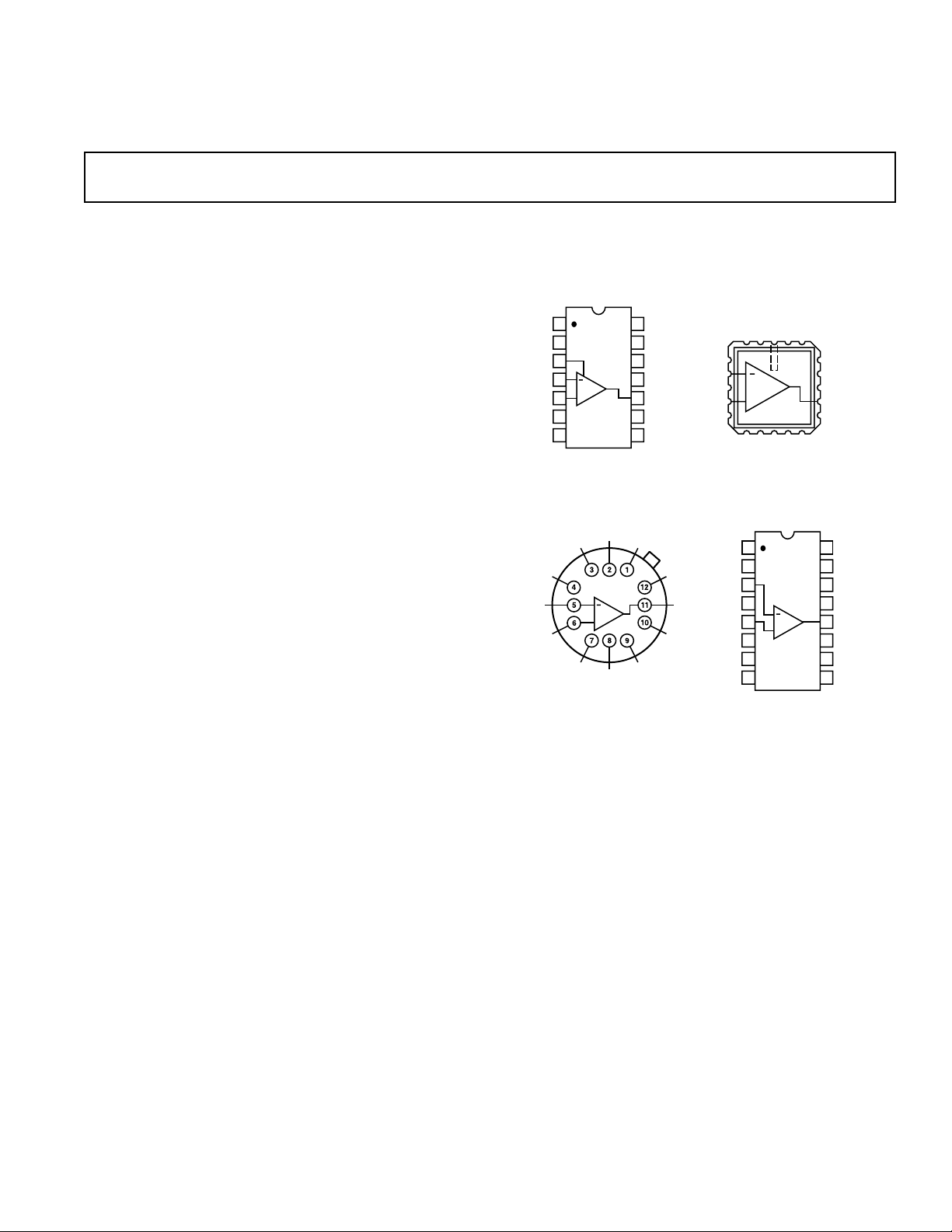
CONNECTION DIAGRAMS
Plastic DIP (N) Package
and
Cerdip (Q) Package
NC
NC
BALANCE
–INPUT
+INPUT
NC
1
AD842
2
3
4
+
5
6
V–
7
TOP VIEW
NC = NO CONNECT
14
NC
13
BALANCE
12
NC
11
V+
10
OUTPUT
9
NC
8
NC
TO-8 (H) Package
NC
BALANCE
BALANCE
NC
V+
AD842
–INPUT
+INPUT
NC
NOTE: CAN BE TIED TO V+
NC = NO CONNECT
+
NC
TOP VIEW
OUTPUT
V–
NC
AD842 is also appropriate for other applications such as high
speed DAC and ADC buffer amplifiers and other wide bandwidth circuitry.
APPLICATION HIGHLIGHTS
1. The high slew rate and fast settling time of the AD842 make
it ideal for DAC and ADC buffers amplifiers, lines drivers
and all types of video instrumentation circuitry.
2. The AD842 is a precision amplifier. It offers accuracy to
0.01% or better and wide bandwidth; performance previously
available only in hybrids.
3. Laser-wafer trimming reduces the input offset voltage of
1 mV max, thus eliminating the need for external offset
nulling in many applications.
4. Full differential inputs provide outstanding performance in
all standard high frequency op amp applications where the
circuit gain will be 2 or greater.
5. The AD842 is an enhanced replacement for the HA2542.
One Technology Way, P.O. Box 9106, Norwood, MA 02062-9106, U.S.A.
Tel: 781/329-4700 World Wide Web Site: http://www.analog.com
Fax: 781/326-8703 © Analog Devices, Inc., 2000
LCC (E) Package
BALANCE
NC
BALANCE
NC
3212019
NC
4
–IN
5
NC
6
+IN
NC
+
7
AD842
8
9
101112
S
NC
NCNCNC
–V
NC = NO CONNECT
SOIC (R-16) Package
1
NC
–INPUT
+INPUT
–V
NC
NC
S
NC
2
AD842
3
4
5
+
6
7
8
TOP VIEW
NC = NO CONNECT
BALANCE
NC
13
NC
18
17
+V
16
NC
OUTPUT
15
14
NC
16
NC
15
BALANCE
14
+V
13
NC
12
OUTPUT
11
NC
10
NC
9
NC
S
S

AD842–SPECIFICATIONS
Model AD842J/JR
(@ +25ⴗC and ⴞ15 V dc, unless otherwise noted)
1
AD842K AD842S
2
Conditions Min Typ Max Min Typ Max Min Typ Max Units
INPUT OFFSET VOLTAGE
3
T
MIN–TMAX
0.5 1.5 0.3 1.0 0.5 1.5 mV
2.5/3 1.5 3.5 mV
Offset Drift 14 14 14 µV/°C
INPUT BIAS CURRENT 4.2 8 3.5 5 4.2 8 µA
T
MIN–TMAX
10 612µA
Input Offset Current 0.1 0.4 0.05 0.2 0.1 0.4 µA
T
MIN–TMAX
0.5 0.3 0.6 µA
INPUT CHARACTERISTICS Differential Mode
Input Resistance 100 100 100 kΩ
Input Capacitance 2.0 2.0 2.0 pF
INPUT VOLTAGE RANGE
Common Mode ⴞ10 ⴞ10 ⴞ10 V
Common-Mode Rejection V
= ±10 V 86 115 90 115 86 115 dB
CM
T
MIN–TMAX
80 86 80 dB
INPUT VOLTAGE NOISE f = 1 kHz 9 9 9 nV/√Hz
Wideband Noise 10 Hz to 10 MHz 28 28 28 µV rms
OPEN-LOOP GAIN V
= ±10 V
O
R
≥ 500 Ω 40/30 90 50 90 40 90 V/mV
LOAD
T
MIN–TMAX
20/15 25 20 V/mV
OUTPUT CHARACTERISTICS
Voltage R
Current V
≥ 500 Ω ⴞ10 ⴞ10 ⴞ10 V
LOAD
= ±10 V 100 100 100 mA
OUT
Open Loop 5 5 5 Ω
FREQUENCY RESPONSE
Gain Bandwidth Product V
Full Power Bandwidth
Rise Time
Overshoot
Slew Rate
5
5
5
Settling Time
4
5
= 90 mV 80 80 80 MHz
OUT
VO = 20 V p-p
R
≥ 500 Ω 4.7 6 4.7 6 4.7 6 MHz
LOAD
A
= –2 10 10 10 ns
VCL
A
= –2 20 20 20 %
VCL
A
= –2 300 375 300 375 300 375 V/µs
VCL
10 V Step
to 0.1% 80 80 80 ns
to 0.01% 100 100 100 ns
Differential Gain f = 4.4 MHz 0.015 0.015 0.015 %
Differential Phase f = 4.4 MHz 0.035 0.035 0.035 Degree
POWER SUPPLY
Rated Performance ±15 ± 15 ±15 V
Operating Range ⴞ5 ⴞ18 ⴞ5 ⴞ18 ⴞ5 ⴞ18 V
Quiescent Current 13/14 14/16 13 14 13 14 mA
Power Supply Rejection Ratio V
TEMPERATURE RANGE
Rated Performance
6
T
MIN–TMAX
= ±5 V to ±18 V 86 100 90 105 86 100 dB
S
T
MIN–TMAX
80 86 80 dB
0 +75 0 +75 –55 +125 °C
16/19.5 16 19 mA
PACKAGE OPTIONS
Plastic (N-14) AD842JN AD842KN
Cerdip (Q-14) AD842JQ AD842KQ AD842SQ, AD842SQ/883B
SOIC (R-16) AD842JR-16
Tape and Reel AD842JR-16-REEL
AD842JR-16-REEL7
TO-8 (H-12A) AD842JH AD842KH AD842SH
LCC (E-20A) AD842SE/883B
Chips AD842JCHIPS AD842SCHIPS
NOTES
1
AD842JR specifications differ from those of the AD842JN, JQ and JH due to the thermal characteristics of the SOIC package.
2
Standard Military Drawing available 5962-8964201xx
2A – (SE/883B); XA – (SH/883B); CA – (SQ/883B).
3
Input offset voltage specifications are guaranteed after 5 minutes at TA = +25°C.
4
Full power bandwidth = slew rate/2 π V
5
Refer to Figures 22 and 23.
6
“S” grade T
All min and max specifications are guaranteed. Specifications shown in boldface are tested on all production units.
Specifications subject to change without notice.
specifications are tested with automatic test equipment at TA = –55°C and TA = +125°C.
MIN–TMAX
PEAK
.
–2–
REV. E

AD842
ABSOLUTE MAXIMUM RATINGS
Supply Voltage . . . . . . . . . . . . . . . . . . . . . . . . . . . . . . . . ±18 V
Internal Power Dissipation
2
1
Plastic (N) . . . . . . . . . . . . . . . . . . . . . . . . . . . . . . . . . 1.3 W
Cerdip (Q) . . . . . . . . . . . . . . . . . . . . . . . . . . . . . . . . . 1.1 W
TO-8 (H) . . . . . . . . . . . . . . . . . . . . . . . . . . . . . . . . . . 1.3 W
SOIC (R) . . . . . . . . . . . . . . . . . . . . . . . . . . . . . . . . . . 1.3 W
LCC (E) . . . . . . . . . . . . . . . . . . . . . . . . . . . . . . . . . . 1.0 W
Input Voltage . . . . . . . . . . . . . . . . . . . . . . . . . . . . . . . . . . . ± V
Differential Input Voltage . . . . . . . . . . . . . . . . . . . . . . . . ±6 V
Storage Temperature Range
Q, H, E . . . . . . . . . . . . . . . . . . . . . . . . . . –65°C to +150°C
N, R . . . . . . . . . . . . . . . . . . . . . . . . . . . . . –65°C to +125°C
Junction Temperature . . . . . . . . . . . . . . . . . . . . . . . . . +175°C
Lead Temperature Range (Soldering 60 sec) . . . . . . . . +300°C
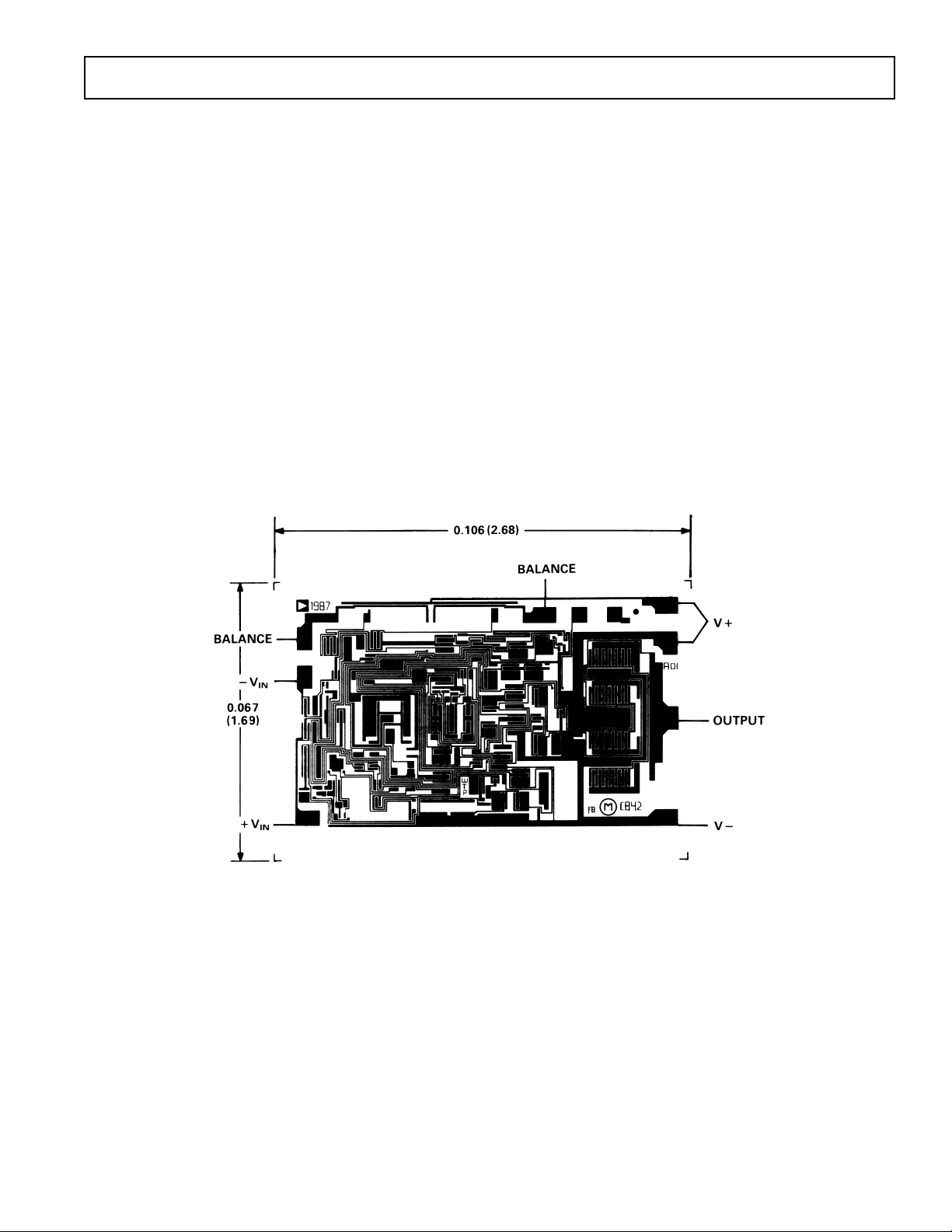
METALIZATION PHOTOGRAPH
Contact factory for latest dimensions.
Dimensions shown in inches and (mm).
NOTES
1
Stresses above those listed under Absolute Maximum Ratings may cause perma-
nent damage to the device. This is a stress rating only; functional operation of the
device at these or any other conditions above those indicated in the operational
section of this specification is not implied. Exposure to absolute maximum rating
conditions for extended periods may affect device reliability.
2
Maximum internal power dissipation is specified so that TJ does not exceed
+150°C at an ambient temperature of +25°C.
Thermal Characteristics:
S
Plastic Package 30°C/W 100°C/W
Cerdip Package 30°C/W 110°C/W 38°C/W
TO-8 Package 30°C/W 100°C/W 27°C/W
16-Lead SOIC Package 30°C/W 100°C/W
20-Lead LCC Package 35°C/W 150°C/W
Recommended Heat Sink: Aavid Engineering© #602B
θ
JC
θ
JA
θ
SA
–3–REV. E
 Loading...