Analog Devices AD8315 b Datasheet
50 dB GSM PA Controller
AD8315
FEATURES
Complete RF Detector/Controller Function
>50 dB Range at 0.9 GHz (–49 dBm to +2 dBm re 50 )
Accurate Scaling from 0.1 GHz to 2.5 GHz
Temperature-Stable Linear-in-dB Response
Log Slope of 23 mV/dB, Intercept at –60 dBm at 0.9 GHz
True Integration Function in Control Loop
Low Power: 20 mW at 2.7 V, 38 mW at 5 V
Power Down to 10.8 W
APPLICATIONS
Single, Dual, and Triple Band Mobile Handset
(GSM, DCS, EDGE)
Transmitter Power Control
PRODUCT DESCRIPTION
The AD8315 is a complete low cost subsystem for the precise
control of RF power amplifiers operating in the frequency range
0.1 GHz–2.5 GHz and over a typical dynamic range of 50 dB. It is
intended for use in cellular handsets and other battery-operated
wireless devices. The log amp technique provides a much wider
measurement range and better accuracy than controllers using
diode detectors. In particular, its temperature stability is excellent
over a specified range of –30∞C to +85∞C.
Its high sensitivity allows control at low signal levels, thus reducing the amount of power that needs to be coupled to the detector.
For convenience, the signal is internally ac-coupled. This
high-pass coupling, with a corner at approximately 0.016 GHz,
determines the lowest operating frequency. Thus, the source
may be dc grounded.
The AD8315 provides a voltage output, VAPC, that has the
voltage range and current drive to directly connect to most handset power amplifiers’ gain control pin. VAPC can swing from 250
mV above ground to within 200 mV below the supply voltage.
Load currents of up to 6 mA can be supported.
The setpoint control input is applied to pin VSET and has an
operating range of 0.25 V–1.4 V. The associated circuit determines the slope and intercept of the linear-in-dB measurement
system; these are nominally 23 mV/dB and –60 dBm for a 50 W
termination (–73 dBV) at 0.9 GHz. Further simplifying the
application of the AD8315, the input resistance of the setpoint
interface is over 100 MW, and the bias current is typically 0.5 mA.
The AD8315 is available in MSOP and lead frame chip scale
(LFCSP) packages and consumes 8.5 mA from a 2.7 V to 5.5 V
supply. When powered down, the sleep current is 4 mA.
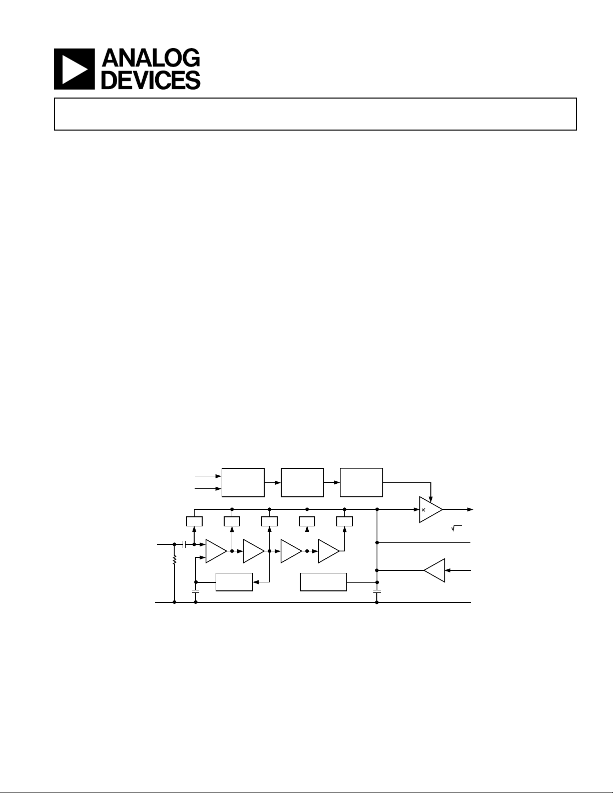
FUNCTIONAL BLOCK DIAGRAM
RFIN
COMM
VPOS
ENBL
LOW NOISE
GAIN BIAS
OFFSET
COMP’N
LOW NOISE
BAND GAP
REFERENCE
10dB10dB10dB
REV. B
Information furnished by Analog Devices is believed to be accurate and
reliable. However, no responsibility is assumed by Analog Devices for its
use, nor for any infringements of patents or other rights of third parties that
may result from its use. No license is granted by implication or otherwise
under any patent or patent rights of Analog Devices. Trademarks and
registered trademarks are the property of their respective companies.
OUTPUT
ENABLE
DELAY
VA PC
1.35
DETDETDETDETDET
10dB
INTERCEPT
POSITIONING
One Technology Way, P.O. Box 9106, Norwood, MA 02062-9106, U.S.A.
Tel: 781/329-4700 www.analog.com
Fax: 781/326-8703 © 2003 Analog Devices, Inc. All rights reserved.
HI-Z
LOW NOISE (25nV/ Hz)
RAIL-TO-RAIL BUFFER
FLTR
VSET
V-I
23mV/dB
250mV to
1.4V = 50dB

AD8315–SPECIFICATIONS
(VS = 2.7 V, T = 25C, 52.3 termination on RFIN, unless otherwise noted.)
Parameter Conditions Min Typ Max Unit
OVERALL FUNCTION
Frequency Range
1
To Meet All Specifications 0.1 2.5 GHz
Input Voltage Range ± 1 dB Log Conformance, 0.1 GHz –57 –11 dBV
Equivalent dBm Range –44 +2 dBm
Logarithmic Slope
Logarithmic Intercept
2
2
0.1 GHz 21.5 24 25.5 mV/dB
0.1 GHz –79 –70 –64 dBV
Equivalent dBm Level –66 –57 –51 dBm
RF INPUT INTERFACE Pin RFIN
Input Resistance
Input Capacitance
3
3
0.1 GHz 2.8 kW
0.1 GHz 0.9 pF
OUTPUT Pin VAPC
Minimum Output Voltage VSET £ 200 mV, ENBL High 0.25 0.27 0.3 V
ENBL Low 0.02 V
Maximum Output Voltage R
vs. Temperature
4
General Limit 2.7 V £ VPOS £ 5.5 V, R
≥ 800 W 2.45 2.6 V
L
85∞C, V
POS
=3 V, I
=6 mA 2.54 V
OUT
= • VPOS – 0.1 V
L
Output Current Drive Source/Sink 5/200 mA/mA
Output Buffer Noise 25 nV÷ Hz
Output Noise RF Input = 2 GHz, 0 dBm, f
= 220 pF
C
FLT
Small Signal Bandwidth 0.2 V to 2.6 V Swing 30 MHz
Slew Rate 10%–90%, 1.2 V Step (V
SET
= 100 kHz, 130 nV/÷Hz
NOISE
), Open Loop
5
13 V/ms
Response Time FLTR = Open, Refer to TPC 24 150 ns
SETPOINT INTERFACE Pin VSET
Nominal Input Range Corresponding to Central 50 dB 0.25 1.4 V
Logarithmic Scale Factor 43.5 dB/V
Input Resistance 100 kW
Slew Rate 16 V/ms
ENABLE INTERFACE Pin ENBL
Logic Level to Enable Power 1.8 V
POS
V
Input Current when Enable High 20 mA
Logic Level to Disable Power 0.8 V
Enable Time Time from ENBL High to V
Final Value, V
£ 200 mV, Refer to TPC 21
SET
Disable Time Time from ENBL Low to V
Final Value, V
£ 200 mV, Refer to TPC 21
SET
Power-On/Enable Time Time from VPOS/ENBL High to V
1% of Final Value, V
£ 200 mV, Refer to
SET
within 1% of 4 5 ms
APC
within 1% of 8 9 ms
APC
within 2 3 ms
APC
TPC 26
Time from VPOS/ENBL Low to V
1% of Final Value, V
£ 200 mV, Refer to
SET
within 100 200 ns
APC
TPC 26
POWER INTERFACE Pin VPOS
Supply Voltage 2.7 5.5 V
Quiescent Current ENBL High 8.5 10.7 mA
Over Temperature –30∞C £ T
Disable Current
6
ENBL Low 4 10 mA
£ +85∞C12.9mA
A
Over Temperature –30∞C £ TA £ +85∞C13mA
NOTES
1
Operation down to 0.02 GHz is possible.
2
Mean and Standard Deviation specifications are available in Table I.
3
See TPC 9 for plot of Input Impedance vs. Frequency.
4
This parameter is guaranteed but not tested in production. Limit is –3 sigma from the mean.
5
Response time in a closed-loop system will depend upon the filter capacitor (C
6
This parameter is guaranteed but not tested in production. Maximum specified limit on this parameter is the +6 sigma value.
Specifications subject to change without notice.
) used and the response of the variable gain element.
FLT
–2–
REV. B
AD8315
Table I. Typical Specifications at Selected Frequencies at 25C (Mean and Sigma)
1 dB Dynamic Range
Slope – mV/dB Intercept – dBV Low Point – dBV High Point – dBV
Frequency – GHz Mean Sigma Mean Sigma Mean Sigma Mean Sigma
0.1 23.8 0.3 –70.1 1.8 –57.7 1.3 –10.6 0.8
0.9 23.2 0.4 –72.6 1.8 –61.0 1.3 –11.2 0.8
1.9 22.2 0.3 –73.8 1.6 –62.9 0.9 –18.5 1.7
2.5 22.3 0.4 –75.6 1.5 –64.0 1.1 –20.0 1.7
ABSOLUTE MAXIMUM RATINGS*
Supply Voltage VPOS . . . . . . . . . . . . . . . . . . . . . . . . . . .5.5 V
Temporary Overvoltage VPOS
(100 cycles, 2 seconds duration, ENBL Low) . . . . . . .6.3 V
VAPC, VSET, ENBL . . . . . . . . . . . . . . . . . . . . . . 0 V, VPOS
RFIN . . . . . . . . . . . . . . . . . . . . . . . . . . . . . . . . . . . . . .17 dBm
Equivalent Voltage . . . . . . . . . . . . . . . . . . . . . . . . 1.6 V rms
Internal Power Dissipation . . . . . . . . . . . . . . . . . . . . . 60 mW
(MSOP) . . . . . . . . . . . . . . . . . . . . . . . . . . . . . . . 200∞C/W
q
JA
q
(LFCSP, Paddle Soldered) . . . . . . . . . . . . . . . . . . 80∞C/W
JA
(LFCSP, Paddle not Soldered) . . . . . . . . . . . . . 200∞C/W
q
JA
Maximum Junction Temperature . . . . . . . . . . . . . . . . . 125∞C
Operating Temperature Range . . . . . . . . . . . –40∞C to +85∞C
Storage Temperature Range . . . . . . . . . . . . –65∞C to +150∞C
Lead Temperature Range (Soldering 60 sec)
MSOP . . . . . . . . . . . . . . . . . . . . . . . . . . . . . . . . . . . . 300∞C
LFCSP . . . . . . . . . . . . . . . . . . . . . . . . . . . . . . . . . . . . 240∞C
*Stresses above those listed under Absolute Maximum Ratings may cause perma-
nent damage to the device. This is a stress rating only; functional operation of the
device at these or any other conditions above those indicated in the operational
section of this specification is not implied. Exposure to absolute maximum rating
conditions for extended periods may affect device reliability.
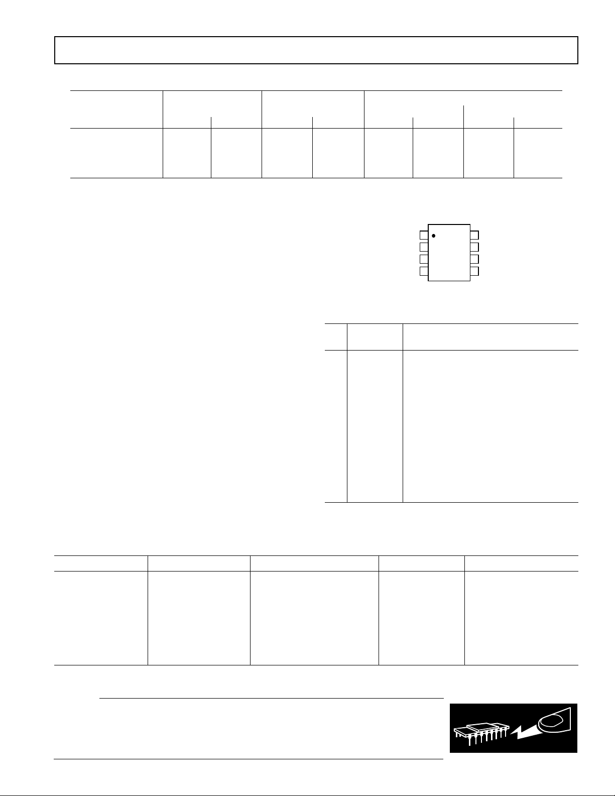
PIN CONFIGURATION
1
RFIN
2
ENBL
3
VSET
(Not to Scale)
4
NC = NO CONNECT
AD8315
TOP VIEW
8
7
6
5
VPOS
VAPC
NC
COMMFLTR
PIN FUNCTION DESCRIPTIONS
Pin
No. Mnemonic Function
1 RFIN RF Input
2 ENBL Connect to VPOS for Normal Operation
Connect pin to ground for Disable Mode
3 VSET Setpoint Input. Nominal input range
0.25 V to 1.4 V.
4 FLTR Integrator Capacitor. Connect between
FLTR and COMM.
5 COMM Device Common (Ground)
6NCNo Connection
7 VAPC Output. Control voltage for gain control
element.
8 VPOS Positive Supply Voltage: 2.7 V to 5.5 V
ORDERING GUIDE
Model Temperature Range Package Descriptions Package Option Branding Information
AD8315ARM –30∞C to +85∞CTube, 8-Lead MSOP RM-8 J7A
AD8315ARM-REEL 13" Tape and Reel
AD8315ARM-REEL7 7" Tape and Reel
AD8315-EVAL MSOP Evaluation Board
AD8315ACP-REEL –30∞C to +85∞C 13" Tape and Reel, CP-8 J7A
8-Lead LFCSP
AD8315ACP-REEL7 7" Tape and Reel
AD8315ACP-EVAL LFCSP Evaluation Board
CAUTION
ESD (electrostatic discharge) sensitive device. Electrostatic charges as high as 4000 V readily
accumulate on the human body and test equipment and can discharge without detection. Although
WARNING!
the AD8315 features proprietary ESD protection circuitry, permanent damage may occur on
devices subjected to high energy electrostatic discharges. Therefore, proper ESD precautions are
recommended to avoid performance degradation or loss of functionality.
REV. B
–3–
ESD SENSITIVE DEVICE
AD8315
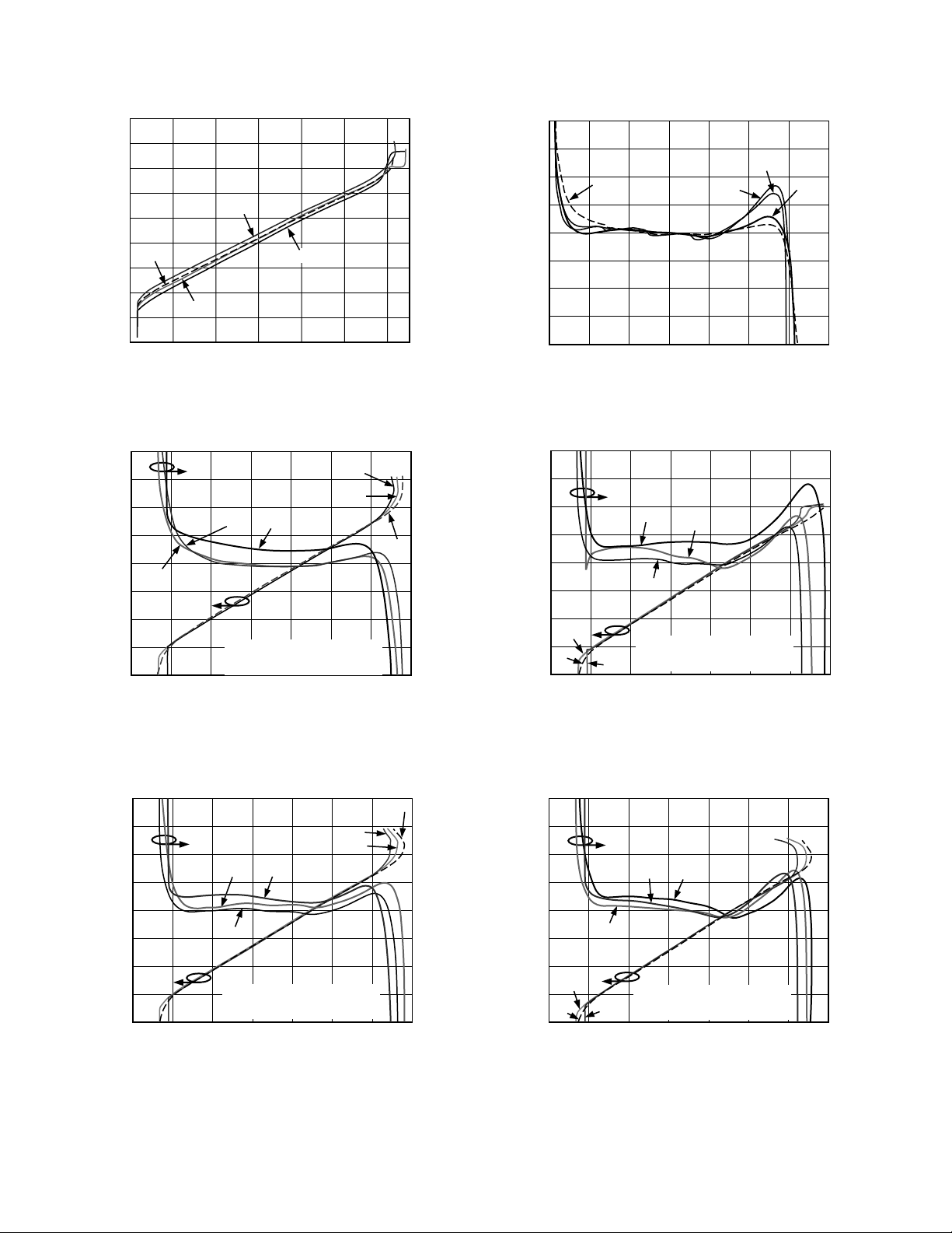
–Typical Performance Characteristics
1
0
–10
–20
–30
–40
0.9GHz
–50
RF INPUT AMPLITUDE – dBV
–60
–70
–80
0.2
10
0
(+3dBm)
–10
–20
–30
RF INPUT
–40
AMPLITUDE – dBV
–50
(–47dBm)
–60
–70
0.1
0.4 0.6 0.8 1.0 1.2 1.4
TPC 1. Input Amplitude vs. V
+25C
0.3 0.5 0.7 0.9 1.1 1.3 1.5
1.9GHz
0.1GHz
2.5GHz
V
– V
SET
SET
–30C
+25C
+85C
–30C
ERROR AT +85C AND –30C
BASED ON DEVIATION FROM
SLOPE AND INTERCEPT AT +25C
V
– V
SET
+85C
TPC 2. Input Amplitude and Log Conformance vs. V
0.1 GHz
23
13
3
–7
–17
–27
–37
–47
RF INPUT AMPLITUDE – dBm
–57
–67
4
3
2
1
0
ERROR – dB
–1
–2
(–47dBm)
TPC 5. Input Amplitude and Log Conformance vs. V
SET
–3
–4
at
1.9 GHz
ERROR – dB
(+3dBm)
–10
–20
–30
RF INPUT
–40
AMPLITUDE – dBV
–50
–60
–70
4
3
2
1
0
–1
–2
–3
–4
0.2
0.1GHz
0.4 0.6 0.8 1.0 1.2 1.4 1.6
V
– V
SET
TPC 4. Log Conformance vs. V
10
0
+85C
+25C
+85C
0.1
–30C
0.3 0.5 0.7 0.9 1.1 1.3 1.5
–30C
+25C
ERROR AT +85C AND –30C
BASED ON DEVIATION FROM
SLOPE AND INTERCEPT AT +25C
V
– V
SET
1.9GHz
2.5GHz
SET
0.9GHz
4
3
2
1
0
–1
–2
–3
–4
SET
ERROR – dB
at
(+3dBm)
RF INPUT
(–47dBm)
10
0
–10
–20
–30
–40
AMPLITUDE – dBV
–50
–60
–70
0.3 0.5 0.7 0.9 1.1 1.3 1.5
0.1
–30C
+25C
–30C
+85C
+25C
ERROR AT +85C AND –30C
BASED ON DEVIATION FROM
SLOPE AND INTERCEPT AT +25C
V
– V
SET
+85C
TPC 3. Input Amplitude and Log Conformance vs. V
0.9 GHz
SET
4
3
2
1
0
ERROR – dB
–1
–2
–3
–4
at
10
0
(+3dBm)
–10
–30C
+85C
ERROR AT +85C AND –30C
BASED ON DEVIATION FROM
SLOPE AND INTERCEPT AT +25C
V
– V
SET
RF INPUT
(–47dBm)
–20
–30
–40
AMPLITUDE – dBV
–50
+25C
–60
–70
0.1
0.3 0.5 0.7 0.9 1.1 1.3 1.5
+25C
–30C+85C
TPC 6. Input Amplitude and Log Conformance vs. V
2.5 GHz
–4–
4
3
2
1
0
ERROR – dB
–1
–2
–3
–4
at
SET
REV. B
AD8315
(
)(
)
(
)(
)
(
)(
)
4
3
2
1
0
ERROR – dB
–1
–2
–3
–4
–80 0–70
+85C
ERROR AT +85C AND –30C
BASED ON DEVIATION FROM
SLOPE AND INTERCEPT AT +25C
–60
RF INPUT AMPLITUDE – dBV
–47dBm
–50 –40 –30 –20 –10
–30C
+3dBm
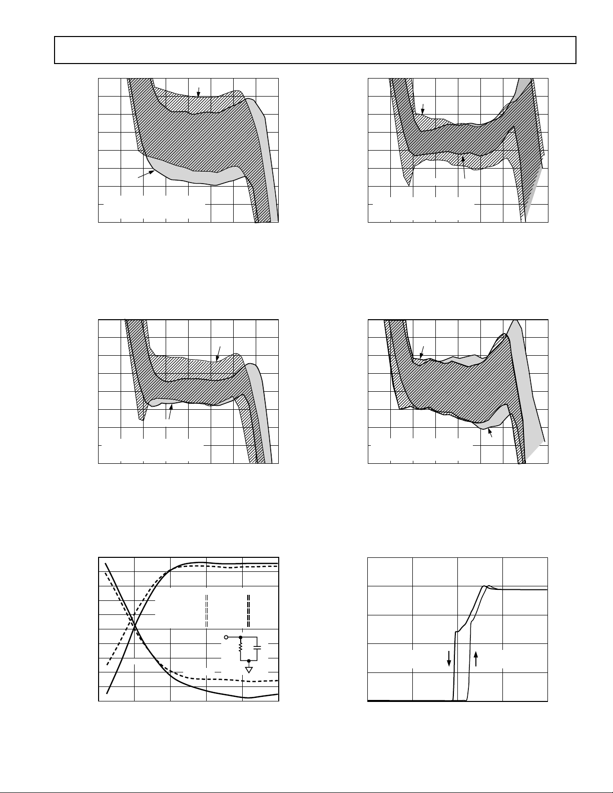
TPC 7. Distribution of Error at Temperature after Ambient
Normalization vs. Input Amplitude, 3 Sigma to Either Side
of Mean, 0.1 GHz
4
3
2
30C
4
3
2
1
0
ERROR – dB
–1
–2
ERROR AT +85C AND –30C
–3
BASED ON DEVIATION FROM
SLOPE AND INTERCEPT AT +25C
–4
–80 0–70
–30C
+85C
–50 –40 –30 –20 –10
–60
RF INPUT AMPLITUDE – dBV
–47dBm
+3dBm
TPC 10. Distribution of Error at Temperature after Ambient
Normalization vs. Input Amplitude, 3 Sigma to Either Side of
Mean, 1.9 GHz
4
3
2
–30C
1
0
ERROR – dB
–1
–2
ERROR AT +85C AND –30C
–3
BASED ON DEVIATION FROM
SLOPE AND INTERCEPT AT +25C
–4
–80 0–70
85C
–60
–50 –40 –30 –20 –10
RF INPUT AMPLITUDE – dBV
(+3dBm)(–47dBm)
TPC 8. Distribution of Error at Temperature after Ambient
Normalization vs. Input Amplitude, 3 Sigma to Either Side
of Mean, 0.9 GHz
jX
j1500
j220
j130
j110
0
–200
–400
–600
–800
–1000
–1200
X
–1400
–1600
–1800
–2000
3000
2700
2400
2100
1800
X (LFCSP)
1500
1200
RESISTANCE –
900
600
300
0
0 2.50.5 1 1.5 2
X (MSOP)
FREQUENCY
(GHz)
0.1
0.9
1.9
2.5
FREQUENCY – GHz
2900 –
R (LFCSP)
R (MSOP)
R –
700 –
130 –
170 –
Chip Scale (LFCSP)
MSOP
jX
j1900
j240
j80
j70
R –
2700 –
730 –
460 –
440 –
R
TPC 9. Input Impedance
1
0
ERROR – dB
–1
–2
ERROR AT +85C AND –30C
–3
BASED ON DEVIATION FROM
SLOPE AND INTERCEPT AT +25C
–4
–80 0–70
–50 –40 –30 –20 –10
–60
RF INPUT AMPLITUDE – dBV
–47dBm
+85C
+3dBm
TPC 11. Distribution of Error at Temperature after Ambient
Normalization vs. Input Amplitude, 3 Sigma to Either Side of
Mean, 2.5 GHz
10
8
REACTANCE –
6
4
DECREASING
SUPPLY CURRENT – mA
2
0
1.3
V
ENBL
1.4 1.5 1.6 1.7
V
ENBL
TPC 12. Supply Current vs. V
– V
INCREASING
V
ENBL
ENBL
REV. B
–5–
AD8315
g
25
24
23
22
SLOPE – mV/dB
21
20
0
–30 C
0.5 1.0 1.5 2.0 2.5
FREQUENCY – GHz
+85 C
+25 C
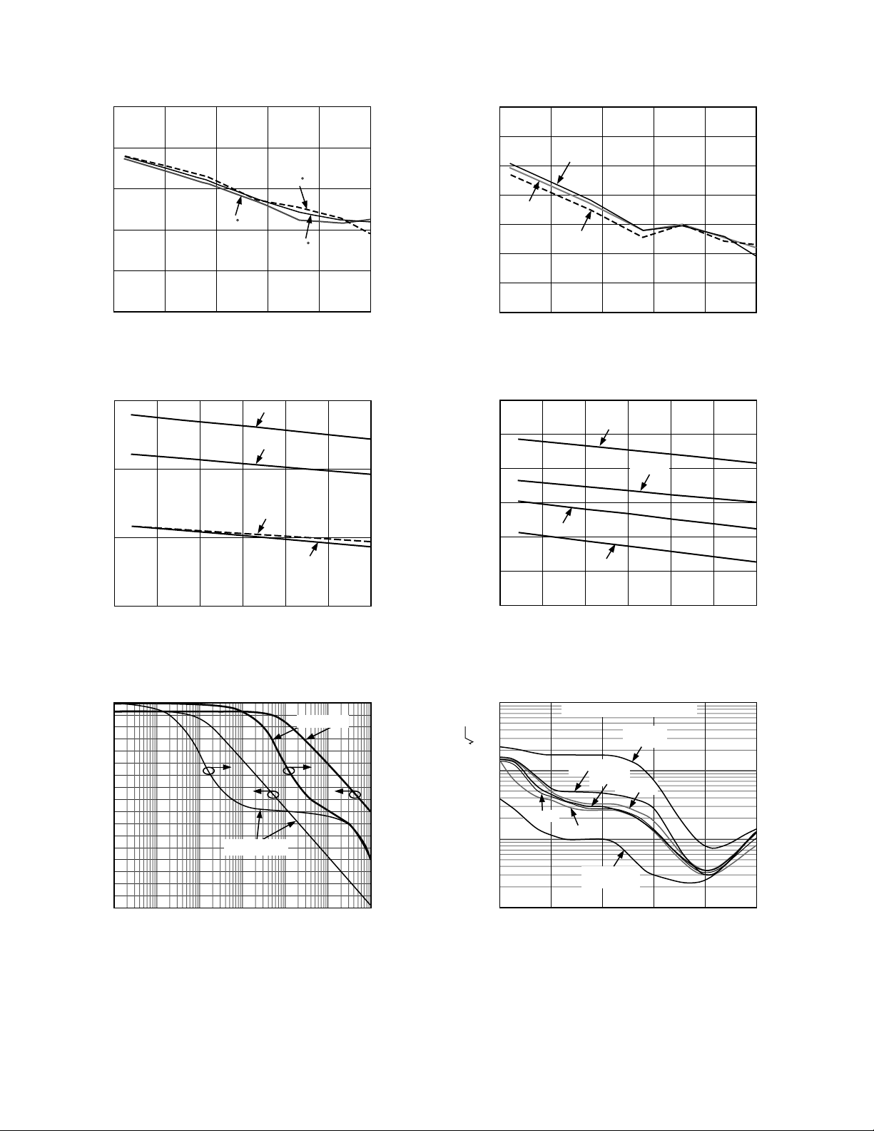
TPC 13. Slope vs. Frequency; –30∞C, +25∞C, and +85∞C
24
23
SLOPE – mV/dB
22
0.1GHz
0.9GHz
1.9GHz
–66
–68
+85 C
–70
–72
+25 C
–74
INTERCEPT – dBV
–76
–78
–80
0
–30 C
0.5 1.0 1.5 2.0 2.5
FREQUENCY – GHz
TPC 16. Intercept vs. Frequency; –30∞C, +25∞C, and +85∞C
–68
–70
–72
–74
INTERCEPT – dBV
–76
0.1GHz
0.9GHz
1.9GHz
2.5GHz
21
3.0 3.5 4.0 4.5 5.0 5.5
2.5
VS – V
TPC 14. Slope vs. Supply Voltage
45
40
35
30
25
20
15
10
5
0
–5
–10
AMPLITUDE – dB
–15
–20
–25
–30
–35
–40
10
100 1k 10k 100k 1M 10M
C
= 220pF
FLT
FREQUENCY – Hz
C
= 0pF
FLT
TPC 15. AC Response from VSET to VAPC
0
–10
–20
–30
–40
–50
–60
–70
–80
–90
–100
–110
–120
–130
rees
PHASE – De
–78
–80
3.0 3.5 4.0 4.5 5.55.0
2.5
2.5GHz
VS – V
TPC 17. Intercept vs. Supply Voltage
10000
1000
100
NOISE SPECTRAL DENSITY – nV/ Hz
10
100
TPC 18. V
C
= 220PF, RF INPUT = 2GHz
FLT
RF INPUT
–51dBV
–48dBV
–33dBV
–43dBV
–23dBV
–13dBV
–53dBV AND
–63dBV
1k 10k 100k 1M 10M
FREQUENCY – Hz
Noise Spectral Density
APC
–6–
REV. B
 Loading...