Analog Devices AD8313 d Datasheet

0.1 GHz to 2.5 GHz 70 dB
FEATURES
Wide bandwidth: 0.1 GHz to 2.5 GHz min
High dynamic range: 70 dB to ±3.0 dB
High accuracy: ±1.0 dB over 65 dB range (@ 1.9 GHz)
Fast response: 40 ns full-scale typical
Controller mode with error output
Scaling stable over supply and temperature
Wide supply range: 2.7 V to 5.5 V
Low power: 40 mW at 3 V
Power-down feature: 60 mW at 3 V
Complete and easy to use
APPLICATIONS
RF transmitter power amplifier setpoint control and
level monitoring
Logarithmic amplifier for RSSI measurement cellular
base stations, radio link, radar
GENERAL DESCRIPTION
The AD8313 is a complete multistage demodulating logarithmic
amplifier that can accurately convert an RF signal at its differential input to an equivalent decibel-scaled value at its dc output.
The AD8313 maintains a high degree of log conformance for
signal frequencies from 0.1 GHz to 2.5 GHz and is useful over
the range of 10 MHz to 3.5 GHz. The nominal input dynamic
range is –65 dBm to 0 dBm (re: 50 Ω), and the sensitivity can be
increased by 6 dB or more with a narrow-band input impedance
matching network or a balun. Application is straightforward,
requiring only a single supply of 2.7 V to 5.5 V and the addition
of a suitable input and supply decoupling. Operating on a 3 V
supply, its 13.7 mA consumption (for T
A power-down feature is provided; the input is taken high to
initiate a low current (20 µA) sleep mode, with a threshold at
half the supply voltage.
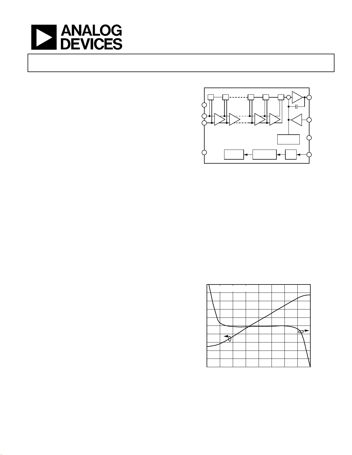
The AD8313 uses a cascade of eight amplifier/limiter cells, each
having a nominal gain of 8 dB and a −3 dB bandwidth of
3.5 GHz. This produces a total midband gain of 64 dB. At each
amplifier output, a detector (rectifier) cell is used to convert the
RF signal to baseband form; a ninth detector cell is placed
directly at the input of the AD8313. The current-mode outputs
of these cells are summed to generate a piecewise linear approximation to the logarithmic function. They are converted to a low
impedance voltage-mode output by a transresistance stage, which
also acts as a low-pass filter.
= 25°C) is only 41 mW.
A
Logarithmic Detector/Controller
AD8313
FUNCTIONAL BLOCK DIAGRAM
NINE DETECTOR CELLS
++ ++
1
VPOS
2
INHI
INLO
3
8dB8dB
EIGHT 8dB 3.5GHz AMPLIFIER STAGES
8dB 8dB
AD8313
4
VPOS
SLOPE
CONTROL
BAND GAP
REFERENCE
Figure 1.
When used as a log amplifier, scaling is determined by a separate
feedback interface (a transconductance stage) that sets the slope
to approximately 18 mV/dB; used as a controller, this stage
accepts the setpoint input. The logarithmic intercept is positioned
to nearly −100 dBm, and the output runs from about 0.45 V dc
at −73 dBm input to 1.75 V dc at 0 dBm input. The scale and
intercept are supply- and temperature-stable.
The AD8313 is fabricated on Analog Devices’ advanced 25 GHz
silicon bipolar IC process and is available in an 8-lead MSOP
package. The operating temperature range is −40°C to +85°C.
An evaluation board is available.
2.0
FREQUENCY = 1.9GHz
1.8
1.6
1.4
1.2
1.0
0.8
0.6
OUTPUT VOLTAGE (V DC)
0.4
0.2
0
–70 –60 –50 –40 –30 –20 –10
–80
Figure 2. Typical Logarithmic Response and Error vs. Input Amplitude
INPUT AMPLITUDE (dBm)
+
I→V
LP
INTERCEPT
CONTROL
GAIN
BIAS
C
V→I
8
VOUT
INT
7
VSET
6
COMM
5
PWDN
01085-C-001
5
4
3
2
1
0
–1
–2
OUTPUT ERROR (dB)
–3
–
4
–5
0
01085-C-002
Rev. D
Information furnished by Analog Devices is believed to be accurate and reliable.
However, no responsibility is assumed by Analog Devices for its use, nor for any
infringements of patents or other rights of third parties that may result from its use.
Specifications subject to change without notice. No license is granted by implication
or otherwise under any patent or patent rights of Analog Devices. Trademarks and
registered trademarks are the property of their respective owners.
One Technology Way, P.O. Box 9106, Norwood, MA 02062-9106, U.S.A.
Tel: 781.329.4700
Fax: 781.326.8703 © 2004 Analog Devices, Inc. All rights reserved.
www.analog.com

AD8313
TABLE OF CONTENTS
Specifications..................................................................................... 3
Input Coupling ........................................................................... 16
Absolute Maximum Ratings............................................................ 6
ESD Caution.................................................................................. 6
Pin Configurations and Function Description............................. 7
Typical Performance Characteristics............................................. 8
Circuit Description......................................................................... 11
Interfaces ..........................................................................................13
Power-Down Interface, PWDN ................................................13
Signal Inputs, INHI, INLO ........................................................ 13
Logarithmic/Error Output, VOUT .......................................... 13
Setpoint Interface, VSET............................................................ 14
Applications..................................................................................... 15
Basic Connections for Log (RSSI) Mode................................. 15
Operating in Controller Mode ................................................. 15
REVISION HISTORY
6/04—Data Sheet Changed from Rev. C to Rev. D
Updated Evaluation Board Section .............................................. 21
Narrow-Band LC Matching Example at 100 MHz ................ 16
Adjusting the Log Slope............................................................. 18
Increasing Output Current........................................................ 19
Effect of Waveform Type on Intercept..................................... 19
Evaluation Board ............................................................................ 20
Schematic and Layout................................................................ 20
General Operation ..................................................................... 20
Using the AD8009 Operational Amplifier.............................. 20
Var yi n g t he L og ar i th m ic S lo p e................................................. 20
Operating in Controller Mode ................................................. 20
RF Burst Response ..................................................................... 20
Outline Dimensions....................................................................... 24
Ordering Guide .......................................................................... 24
2/03—Data Sheet changed from Rev. B to Rev. C
TPCs and Figures Renumbered........................................Universal
Edits to SPECIFICATIONS............................................................. 2
Updated ESD CAUTION ................................................................ 4
Updated OUTLINE DIMENSIONS .............................................. 7
8/99—Data Sheet changed from Rev. A to Rev. B
5/99—Data Sheet changed from Rev. 0 to Rev. A
8/98—Revision 0: Initial Version
Rev. D | Page 2 of 24

AD8313
SPECIFICATIONS
TA = 25°C, VS = 5 V1, RL 10 kΩ, unless otherwise noted.
Table 1.
Parameter Conditions Min
SIGNAL INPUT INTERFACE
Specified Frequency Range 0.1 2.5 GHz
DC Common-Mode Voltage V
Input Bias Currents 10 µA
Input Impedance fRF < 100 MHz
LOG (RSSI) MODE
Sinusoidal, input termination configuration
3
shown in Figure 29
100 MHz
5
±3 dB Dynamic Range
6
53.5 65 dB
Nominal conditions
Range Center −31.5 dBm
±1 dB Dynamic Range 56 dB
Slope 17 19 21 mV/dB
Intercept −96 −88 −80 dBm
2.7 V ≤ VS ≤ 5.5 V, −40°C ≤ T ≤ +85°C
±3 dB Dynamic Range 51 64 dB
Range Center −31 dBm
±1 dB Dynamic Range 55 dB
Slope 16 19 22 mV/dB
Intercept −99 −89 −75 dBm
Temperature Sensitivity PIN = −10 dBm −0.022 dB/°C
900 MHz
5
Nominal conditions
±3 dB Dynamic Range 60 69 dB
Range Center −32.5 dBm
±1 dB Dynamic Range 62 dB
Slope 15.5 18 20.5 mV/dB
Intercept −105 −93 −81 dBm
2.7 V ≤ VS ≤ 5.5 V, –40°C ≤ T ≤ +85°C
±3 dB Dynamic Range 55.5 68.5 dB
Range Center –32.75 dBm
±1 dB Dynamic Range 61 dB
Slope 15 18 21 mV/dB
Intercept –110 –95 –80 dBm
Temperature Sensitivity PIN = –10 dBm –0.019 dB/°C
1.9 GHz7 Nominal conditions
±3 dB Dynamic Range 52 73 dB
Range Center –36.5 dBm
±1 dB Dynamic Range 62 dB
Slope 15 17.5 20.5 mV/dB
Intercept –115 –100 –85 dBm
2.7 V ≤ VS ≤ 5.5 V, –40°C ≤ T ≤ +85°C
±3 dB Dynamic Range 50 73 dB
Range Center –36.5 dBm
±1 dB Dynamic Range 60 dB
Slope 14 17.5 21.5 mV/dB
Intercept –125 –101 –78 dBm
Temperature Sensitivity PIN = –10 dBm –0.019 dB/°C
2
Typ Max
– 0.75 V
POS
900||1.1 Ω||pF
2
Unit
4
Rev. D | Page 3 of 24

AD8313
Parameter Conditions Min
7
2.5 GHz
Nominal conditions
2
Typ Max
2
Unit
±3 dB Dynamic Range 48 66 dB
Range Center –34 dBm
±1 dB Dynamic Range 46 dB
Slope 16 20 25 mV/dB
Intercept –111 –92 –72 dBm
2.7 V ≤ VS ≤ 5.5 V, –40°C ≤ T ≤ +85°C
±3 dB Dynamic Range 47 68 dB
Range Center –34.5 dBm
±1 dB Dynamic Range 46 dB
Slope 14.5 20 25 mV/dB
Intercept –128 –92 –56 dBm
Temperature Sensitivity PIN =–10 dBm –0.040 dB/°C
5
3.5 GHz
Nominal conditions
±3 dB Dynamic Range 43 dB
±1 dB Dynamic Range 35 dB
Slope 24 mV/dB
Intercept –65 dBm
CONTROL MODE
Controller Sensitivity f = 900 MHz 23 V/dB
Low Frequency Gain VSET to VOUT8 84 dB
Open-Loop Corner Frequency VSET to VOUT
8
700 Hz
Open-Loop Slew Rate f = 900 MHz 2.5 V/µs
VSET Delay Time 150 ns
VOUT INTERFACE
Current Drive Capability
Source Current 400 µA
Sink Current 10 mA
Minimum Output Voltage Open-loop 50 mV
Maximum Output Voltage Open-loop V
Output Noise Spectral Density PIN = –60 dBm, f
P
= –60 dBm, f
IN
= 100 Hz 2.0 µV/√Hz
SPOT
= 10 MHz 1.3 µV/√Hz
SPOT
– 0.1 V
POS
Small Signal Response Time PIN = –60 dBm to –57 dBm, 10% to 90% 40 60 ns
Large Signal Response Time PIN = No signal to 0 dBm; settled to 0.5 dB 110 160 ns
VSET INTERFACE
Input Voltage Range 0 V
POS
V
Input Impedance 18||1 kΩ||pF4
POWER-DOWN INTERFACE
PWDN Threshold V
Power-Up Response Time
Time delay following high to low transition
1.8 µs
/2 V
POS
until device meets full specifications.
PWDN Input Bias Current PWDN = 0 V 5 µA
PWDN = VS <1 µA
POWER SUPPLY
Operating Range 2.7 5.5 V
Powered-Up Current 13.7 15.5 mA
4.5 V ≤VS ≤ 5.5 V, –40°C ≤ T ≤ +85°C 18.5 mA
2.7 V ≤VS ≤ 3.3 V, –40°C ≤ T ≤ +85°C 18.5 mA
Powered-Down Current 4.5 V ≤VS ≤ 5.5 V, –40°C ≤ T ≤ +85°C 50 150 µA
2.7 V ≤VS ≤ 3.3 V, –40°C ≤ T ≤ +85°C 20 50 µA
Rev. D | Page 4 of 24

AD8313
1
Except where otherwise noted; performance at VS = 3 V is equivalent to 5 V operation.
2
Minimum and maximum specified limits on parameters that are guaranteed but not tested are 6 sigma values.
3
Input impedance shown over frequency range in Figure 26.
4
Double vertical bars (||) denote “in parallel with.”
5
Linear regression calculation for error curve taken from –40 dBm to –10 dBm for all parameters.
6
Dynamic range refers to range over which the linearity error remains within the stated bound.
7
Linear regression calculation for error curve taken from –60 dBm to –5 dBm for 3 dB dynamic range. All other regressions taken from –40 dBm to –10 dBm.
8
AC response shown in Figure 12.
Rev. D | Page 5 of 24

AD8313
ABSOLUTE MAXIMUM RATINGS
Table 2.
Supply Voltage V
VOUT, VSET, PWDN 0 V, VPOS
Input Power Differential (re: 50 Ω, 5.5 V) 25 dBm
Input Power Single-Ended (re: 50 Ω, 5.5 V) 19 dBm
Internal Power Dissipation 200 mW
θ
JA
Maximum Junction Temperature 125°C
Operating Temperature Range –40°C to +85°C
Storage Temperature Range –65°C to +150°C
S
5.5 V
200°C/W
ESD CAUTION
ESD (electrostatic discharge) sensitive device. Electrostatic charges as high as 4000 V readily accumulate on
the human body and test equipment and can discharge without detection. Although this product features
proprietary ESD protection circuitry, permanent damage may occur on devices subjected to high energy
electrostatic discharges. Therefore, proper ESD precautions are recommended to avoid performance
degradation or loss of functionality.
Stresses above those listed under Absolute Maximum Ratings
may cause permanent damage to the device. This is a stress
rating only; functional operation of the device at these or any
other conditions above those indicated in the operational
section of this specification is not implied. Exposure to absolute
maximum rating conditions for extended periods may affect
device reliability.
Rev. D | Page 6 of 24

AD8313
V
V
PIN CONFIGURATIONS AND FUNCTION DESCRIPTION
POS
1
INHI
INLO
POS
AD8313
2
TOP VIEW
3
(Not to Scale)
4
Figure 3. Pin Configuration
Table 3. Pin Function Descriptions
Pin No. Mnemonic Description
1, 4 VPOS Positive Supply Voltage (VPOS), 2.7 V to 5.5 V.
2 INHI Noninverting Input. This input should be ac-coupled.
3 INLO Inverting Input. This input should be ac-coupled.
5 PWDN Connect Pin to Ground for Normal Operating Mode. Connect this pin to the supply for power-down mode.
6 COMM Device Common.
7 VSET Setpoint Input for Operation in Controller Mode. To operate in RSSI mode, short VSET and VOUT.
8 VOUT Logarithmic/Error Output.
VOUT
8
VSET
7
6
COMM
PWDN
5
01085-C-003
Rev. D | Page 7 of 24

AD8313
TYPICAL PERFORMANCE CHARACTERISTICS
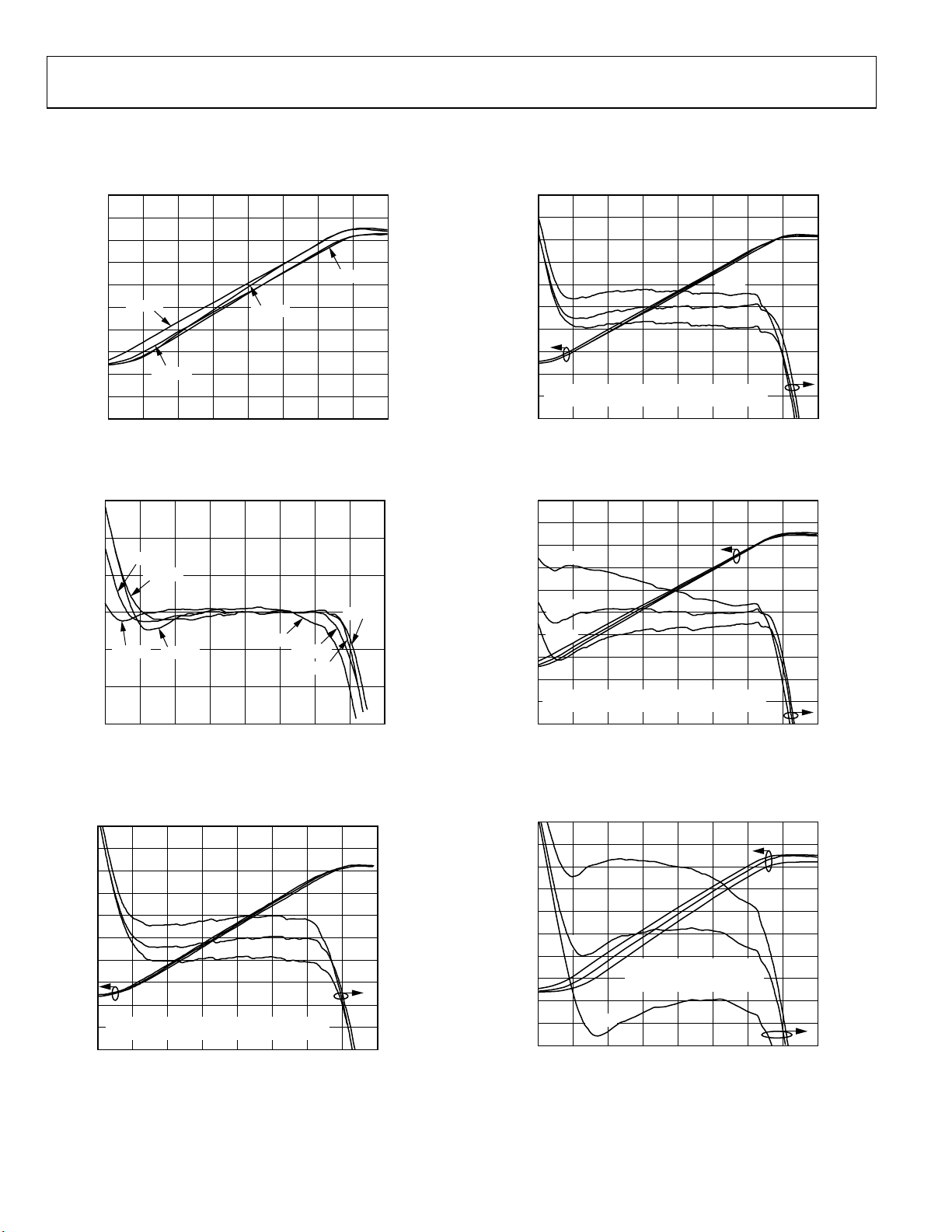
TA = 25°C, VS = 5 V, RL input match shown in Figure 29, unless otherwise noted.
2.0
1.8
1.6
1.4
1.2
(V)
1.0
OUT
V
0.8
0.6
0.4
0.2
0
–70
6
4
2
0
ERROR (dB)
–2
1.9GHz
–4
–6
–70 10–60
1.9GHz
900MHz
–60 –50 –40 –30 –20 –10 0 10
INPUT AMPLITUDE (dBm)
Figure 4. V
900MHz
100MHz
2.5GHz
–50 –40 –30 –20 –10
INPUT AMPLITUDE (dBm)
2.5GHz
vs. Input Amplitude
OUT
2.5GHz
100MHz
1.9GHz
100MHz
900MHz
0
01085-C-004
01085-C-005
2.0
1.8
1.6
1.4
1.2
(V)
1.0
OUT
V
0.8
0.6
0.4
SLOPE AND INTERCEPT NORMALIZED AT +25°C
0.2
AND APPLIED TO –40°C AND +85°C
0
–60 –50 –40 –30 –20 –10 0 10
–70
Figure 7. V
and Log Conformance vs. Input Amplitude at 900 MHz for
OUT
INPUT AMPLITUDE (dBm)
Multiple Temperatures
2.0
1.8
1.6
–40°C
1.4
1.2
(V)
+25°C
1.0
OUT
V
0.8
+85°C
0.6
0.4
SLOPE AND INTERCEPT NORMALIZED AT +25°C
0.2
AND APPLIED TO –40°C AND +85°C
0
–60 –50 –40 –30 –20 –10 0 10
–70
INPUT AMPLITUDE (dBm)
–40°C
+25°C
+85°C
5
4
3
2
1
0
–1
–2
–3
–4
–5
5
4
3
2
1
0
–1
–2
–3
–4
–5
ERROR (dB)
01-85-C-007
ERROR (dB)
01085-C-008
Figure 5. Log Conformance vs. Input Amplitude
2.0
1.8
1.6
1.4
1.2
(V)
1.0
OUT
V
0.8
0.6
0.4
SLOPE AND INTERCEPT NORMALIZED AT +25°C
0.2
AND APPLIED TO –40°C AND +85°C
0
–60 –50 –40 –30 –20 –10 0 10
–70
Figure 6. V
OUT
INPUT AMPLITUDE (dBm)
and Log Conformance vs. Input Amplitude at 100 MHz for
Multiple Temperatures
Figure 8. V
(V)
V
OUT
2.0
1.8
1.6
1.4
1.2
1.0
0.8
0.6
0.4
0.2
–40°C
+25°C
+85°C
5
4
3
2
1
0
–1
–2
–3
–4
–5
ERROR (dB)
01085-C-006
Figure 9. V
and Log Conformance vs. Input Amplitude at 1.9 GHz for
OUT
Multiple Temperatures
–40°C
+25°C
SLOPE AND INTERCEPT
NORMALIZED AT +25°C AND
APPLIED TO –40°C AND +85°C
+85°C
0
–60 –50 –40 –30 –20 –10 0 10
–70
and Log Conformance vs. Input Amplitude at 2.5 GHz for
OUT
INPUT AMPLITUDE (dBm)
5
4
3
2
1
0
–1
–2
–3
–4
–5
ERROR (dB)
01085-C-009
Multiple Temperatures
Rev. D | Page 8 of 24
 Loading...