Analog Devices AD8307AR-REEL7, AD8307AR-REEL, AD8307AR, AD8307AN, AD8307-EB Datasheet
Low Cost DC-500 MHz, 92 dB
a
FEATURES
Complete Multistage Logarithmic Amplifier
92 dB Dynamic Range: –75 dBm to +17 dBm
to –90 dBm Using Matching Network
Single Supply of 2.7 V Min at 7.5 mA Typical
DC-500 MHz Operation, ⴞ1 dB Linearity
Slope of 25 mV/dB, Intercept of –84 dBm
Highly Stable Scaling Over Temperature
Fully Differential DC-Coupled Signal Path
100 ns Power-Up Time, 150 A Sleep Current
APPLICATIONS
Conversion of Signal Level to Decibel Form
Transmitter Antenna Power Measurement
Receiver Signal Strength Indication (RSSI)
Low Cost Radar and Sonar Signal Processing
Network and Spectrum Analyzers (to 120 dB)
Signal Level Determination Down to 20 Hz
True Decibel AC Mode for Multimeters
Logarithmic Amplifier
AD8307
FUNCTIONAL BLOCK DIAGRAM
SUPPLY ENABLE
+INPUT
–INPUT
COMMON
VPS
INP
1.15kV
INM
COM
BANDGAP REFERENCE
7.5mA
SIX 14.3dB 900MHz
AMPLIFIER STAGES
3
NINE DETECTOR CELLS
SPACED 14.3dB
INPUT-OFFSET
COMPENSATION LOOP
AD8307
AND BIASING
MIRROR
2mA
/dB
2
COM
ENB
INT
OUT
12.5kV
OFS
INT. ADJ
OUTPUT
OFS. ADJ.
PRODUCT DESCRIPTION
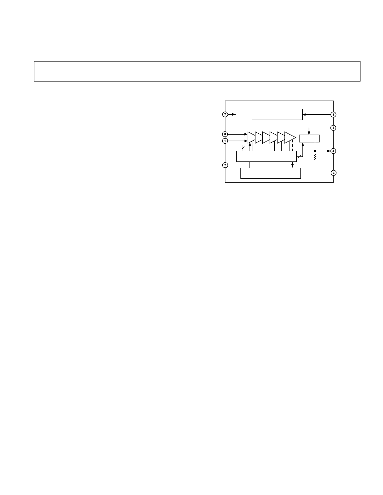
The AD8307 is the first logarithmic amplifier in an 8-lead (SO-8)
package. It is a complete 500 MHz monolithic demodulating
logarithmic amplifier based on the progressive compression
(successive detection) technique, providing a dynamic range of
92 dB to ±3 dB law-conformance and 88 dB to a tight ±1 dB
error bound at all frequencies up to 100 MHz. It is extremely
stable and easy to use, requiring no significant external components. A single supply voltage of 2.7 V to 5.5 V at 7.5 mA is
needed, corresponding to an unprecedented power consumption
of only 22.5 mW at 3 V. A fast-acting CMOS-compatible control pin can disable the AD8307 to a standby current of under
150 µA.
Each of the cascaded amplifier/limiter cells has a small-signal
gain of 14.3 dB, with a –3 dB bandwidth of 900 MHz. The
input is fully differential and at a moderately high impedance
(1.1 kΩ in parallel with about 1.4 pF). The AD8307 provides a
basic dynamic range extending from approximately –75 dBm
(where dBm refers to a 50 Ω source, that is, a sine amplitude of
about ±56 µV) up to +17 dBm (a sine amplitude of ±2.2 V).
A simple input-matching network can lower this range to –88dBm
to +3 dBm. The logarithmic linearity is typically within ±0.3 dB
up to 100 MHz over the central portion of this range, and is
degraded only slightly at 500 MHz. There is no minimum
frequency limit; the AD8307 may be used at audio frequencies
(20 Hz) or even lower.
The output is a voltage scaled 25 mV/dB, generated by a current
of nominally 2 µA/dB through an internal 12.5 kΩ resistor. This
voltage varies from 0.25 V at an input of –74 dBm (that is, the
ac intercept is at –84 dBm, a 20 µV rms sine input), up to 2.5 V
for an input of +16 dBm. This slope and intercept can be trimmed
using external adjustments. Using a 2.7 V supply, the output
scaling may be lowered, for example to 15 mV/dB, to permit
utilization of the full dynamic range.
The AD8307 exhibits excellent supply insensitivity and temperature stability of the scaling parameters. The unique combination of low cost, small size, low power consumption, high
accuracy and stability, very high dynamic range, and a frequency
range encompassing audio through IF to UHF, make this product useful in numerous applications requiring the reduction of a
signal to its decibel equivalent.
The AD8307 is available in the industrial temperature range of
–40°C to +85°C, and in 8-lead SOIC and PDIP packages.
REV. A
Information furnished by Analog Devices is believed to be accurate and
reliable. However, no responsibility is assumed by Analog Devices for its
use, nor for any infringements of patents or other rights of third parties
which may result from its use. No license is granted by implication or
otherwise under any patent or patent rights of Analog Devices.
One Technology Way, P.O. Box 9106, Norwood, MA 02062-9106, U.S.A.
Tel: 781/329-4700 World Wide Web Site: http://www.analog.com
Fax: 781/326-8703 © Analog Devices, Inc., 1999

AD8307–SPECIFICA TIONS
(VS = +5 V, TA = 25ⴗC, RL ≥ 1M⍀, unless otherwise noted)
Parameter Conditions Min Typ Max Units
GENERAL CHARACTERISTICS
Input Range (±1 dB Error) Expressed in dBm re 50 Ω –72 16 dBm
Logarithmic Conformance f ≤ 100 MHz, Central 80 dB ±0.3 ±1dB
f = 500 MHz, Central 75 dB ±0.5 dB
Logarithmic Slope Unadjusted
vs. Temperature 23 27 mV/dB
Logarithmic Intercept Sine Amplitude; Unadjusted
1
2
23 25 27 mV/dB
20 µV
Equivalent Sine Power in 50 Ω –87 –84 –77 dBm
vs. Temperature –88 –76 dBm
Input Noise Spectral Density Inputs Shorted 1.5 nV/√Hz
Operating Noise Floor R
= 50 Ω/2 –78 dBm
SOURCE
Output Resistance Pin 4 to Ground 10 12.5 15 kΩ
Internal Load Capacitance 3.5 pF
Response Time Small Signal, 10%-90%, 400 ns
0 mV–100 mV, C
= 2 pF
L
Large Signal, 10%-90%, 500 ns
= 2 pF
L
500 MHz
Upper Usable Frequency
3
0 V–2.4 V, C
Lower Usable Frequency Input AC-Coupled 10 Hz
AMPLIFIER CELL CHARACTERISTICS
Cell Bandwidth –3 dB 900 MHz
Cell Gain 14.3 dB
INPUT CHARACTERISTICS
DC Common-Mode Voltage Inputs AC-Coupled 3.2 V
Common-Mode Range Either Input (Small Signal) –0.3 1.6 VS – 1 V
DC Input Offset Voltage
4
R
SOURCE
≤ 50 Ω 50 500 µV
Drift 0.8 µV/°C
Incremental Input Resistance Differential 1.1 kΩ
Input Capacitance Either Pin to Ground 1.4 pF
Bias Current Either Input 10 25 µA
POWER INTERFACES
Supply Voltage 2.7 5.5 V
Supply Current V
Disabled V
NOTES
1
This may be adjusted downward by adding a shunt resistor from the Output to Ground. A 50 kΩ resistor will reduce the nominal slope to 20 mV/dB.
2
This may be adjusted in either direction by a voltage applied to Pin 5, with a scale factor of 8 dB/V.
3
See Application on 900 MHz operation.
4
Normally nulled automatically by internal offset correction loop. May be manually nulled by a voltage applied between Pin 3 and Ground; see APPLICATIONS.
Specifications subject to change without notice.
≥ 2 V 8 10 mA
ENB
≤ 1 V 150 750 µA
ENB
–2–
REV. A
AD8307
ABSOLUTE MAXIMUM RATINGS*
Supply Voltage . . . . . . . . . . . . . . . . . . . . . . . . . . . . . . . +7.5 V
Input Voltage (Pins 1, 8) . . . . . . . . . . . . . . . . . . . . . . V
SUPPLY
Storage Temperature Range, N, R . . . . . . . . –65°C to +125°C
*Stresses above those listed under Absolute Maximum Ratings may cause perma-
nent damage to the device. This is a stress rating only; functional operation of the
device at these or any other conditions above those indicated in the operational
section of this specification is not implied. Exposure to absolute maximum rating
conditions for extended periods may effect device reliability.
Ambient Temperature Range, Rated Performance Industrial,
AD8307AN, AD8307AR . . . . . . . . . . . . . –40°C to +85°C
Lead Temperature Range (Soldering 10 sec) . . . . . . . +300°C
ORDERING GUIDE
Model Temperature Range Package Descriptions Package Options
AD8307AR –40°C to +85°C SOIC SO-8
AD8307AN –40°C to +85°C Plastic DIP N-8
AD8307AR-REEL 13" REEL
AD8307AR-REEL7 7" REEL
AD8307-EB Evaluation Board
CAUTION
ESD (electrostatic discharge) sensitive device. Electrostatic charges as high as 4000 V readily
accumulate on the human body and test equipment and can discharge without detection. Although
WARNING!
the AD8307 features proprietary ESD protection circuitry, permanent damage may occur on
devices subjected to high energy electrostatic discharges. Therefore, proper ESD precautions are
recommended to avoid performance degradation or loss of functionality.
ESD SENSITIVE DEVICE
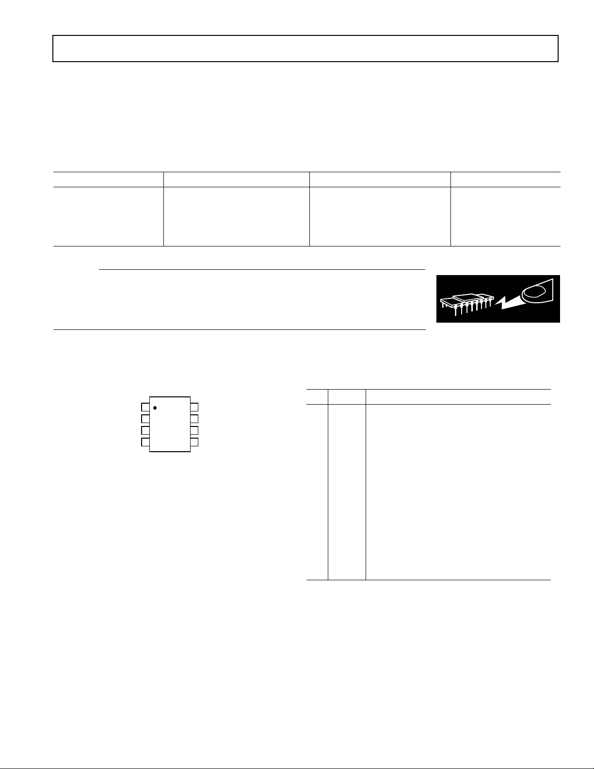
PIN CONFIGURATION
INM
COM
OFS
OUT
1
2
AD8307
TOP VIEW
3
(Not to Scale)
4
8
INP
7
VPS
6
ENB
5
INT
PIN FUNCTION DESCRIPTIONS
Pin Name Function
1 INM Signal Input, Minus Polarity; Normally at
V
/2.
POS
2 COM Common Pin (Usually Grounded).
3 OFS Offset Adjustment; External Capacitor
Connection.
4 OUT Logarithmic (RSSI) Output Voltage; R
OUT
=
12.5 kΩ.
5 INT Intercept Adjustment; ±6 dB (See Text).
6 ENB CMOS-compatible Chip Enable; Active when
“HI.”
7 VPS Positive Supply, 2.7 V–5.5 V.
8 INP Signal Input, Plus Polarity; Normally at V
POS
/
2. Note: Due to the symmetrical nature of the
response, there is no special significance to the
sign of the two input pins. DC resistance from
INP to INM = 1.1 kΩ.
–3–REV. A
AD8307–T ypical Performance Characteristics
8
7
6
5
4
3
SUPPLY CURRENT – mA
2
1
0
1.0
1.1
1.2
1.3
1.4
1.5
ENB
1.6
– Volts
V
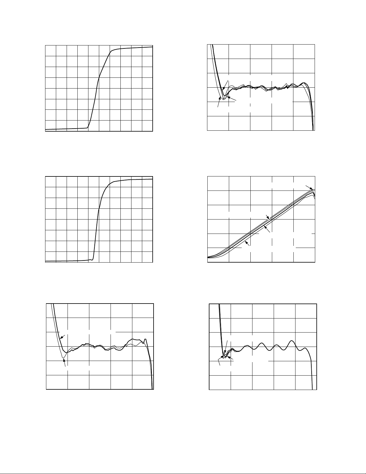
Figure 1. Supply Current vs. V
8
7
6
5
4
3
SUPPLY CURRENT – mA
2
1
1.7
1.8
Voltage (5 V)
ENB
1.9
2.0
3
2
1
0
ERROR – dB
–1
–2
–3
–80
TEMPERATURE ERROR @ +858C
TEMPERATURE ERROR @ +258C
TEMPERATURE ERROR @ –408C
–40 –20 0
INPUT LEVEL – dBm
20–60
Figure 4. Log Conformance vs. Input Level (dBm) at 25°C,
°
C, –40°C
85
3
INPUT FREQUENCY 10MHz
2
INPUT FREQUENCY 100MHz
– Volts
OUT
V
1
INPUT FREQUENCY 300MHz
INPUT FREQUENCY 500MHz
0
1.0
1.1
1.2
1.3
1.4
1.5
V
– Volts
ENB
Figure 2. Supply Current vs. V
3
2
1
0
ERROR – dB
–1
–2
–3
FREQUENCY INPUT = 300MHz
FREQUENCY INPUT = 100MHz
–80 20–60
INPUT LEVEL – dBm
–40 –20 0
1.7
1.6
Voltage (3 V)
ENB
1.8
1.9
2.0
Figure 3. Log Conformance vs. Input Level (dBm) @
100 MHz, 300 MHz
0
–80
Figure 5. V
1.5
1.0
0.5
0
ERROR – dB
–0.5
–1.0
– 1.5
vs. Input Level (dBm) at Various Frequencies
OUT
CFO VALUE = 0.01mF
CFO VALUE = 0.1mF
– 80 20– 60
–40 –20 0
INPUT LEVEL – dBm
CFO VALUE = 1mF
– 40 – 20 0
INPUT LEVEL – dBm
20–60
Figure 6. Log Conformance vs. CFO Values at 1 kHz Input
Frequency
–4–
REV. A
3.0
INPUT LEVEL – dBm
3
2
–3
–80 20–60
ERROR – dB
–40 –20 0
1
0
–1
–2
– INPUT
+ INPUT
100MHz
INPUT LEVEL – dBm
3
2
–3
–70 10–60
ERROR – dB
–50 –40 –30
1
0
–1
–2
100MHz
500MHz
20–20 –10 0
10MHz
AD8307
2.5
2.0
INT PIN = 4.0V
10MHz, INT = –87.71dBm
1.5
– Volts
OUT
V
1.0
0.5
0
–80
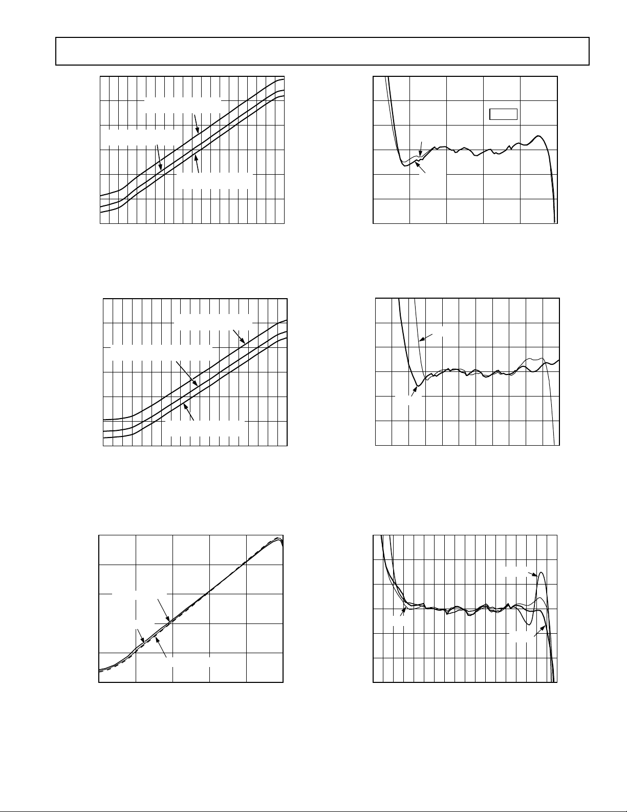
Figure 7. V
–70 –50 –30 –10 10
OUT
10MHz, INT = –96.52dBm
vs. Input Level at 5 V Supply; Showing
Intercept Adjustment
3.0
2.5
2.0
INT VOLTAGE
INT NO CONNECT, INT = –71dBm
1.5
– Volts
OUT
V
1.0
INT PIN = 3.0V
NO CONNECT ON INT
10MHz, INT = –82.90dBm
INPUT LEVEL – dBm
–20 0
INT = 1.0V, INT = –86dBm
INT VOLTAGE
20–60 –40
Figure 10. Log Conformance vs. Input Level at 100 MHz;
Showing Response to Alternative Inputs
3
2
1
0
ERROR – dB
–1
100MHz
500MHz
0.5
0
–80 –70 –60 –50 –40 –30 –20 –10
Figure 8. V
vs. Input Level at 3 V Supply Using AD820
OUT
INT VOLTAGE
INT = 2.0V, INT = –78dBm
INPUT LEVEL – dBm
010
as Buffer, Gain = +2; Showing Intercept Adjustment
2.5
2.0
1.5
100MHz @ –408C
– Volts
OUT
1.0
100MHz @ +258C
V
0.5
100MHz @ +858C
0
–80 20–60
Figure 9. V
(–40
°
C, +25°C, +85°C)
OUT
–40 –20 0
INPUT LEVEL – dBm
vs. Input Level at Three Temperatures
–2
–3
–90 10–70
–50 –30 –10
INPUT LEVEL – dBm
Figure 11. Log Conformance vs. Input at 100 MHz, 500 MHz;
Input Driven Differentially Using Transformer
Figure 12. Log Conformance vs. Input Level at 3 V Supply
Using AD820 as Buffer, Gain = +2
–5–REV. A
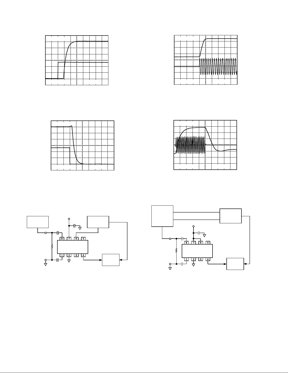
AD8307
Ch1 200mV
GND
500nsCh2 2.00V
Figure 13. Power-Up Response Time
Ch1 200mV
V
OUT
CH 1
V
ENB
CH 2
GND
500nsCh2 2.00V
V
OUT
CH 1
V
ENB
CH 2
CH 1 GND
INPUT SIGNAL
CH 2
2.5V
INPUT SIGNAL
CH 2
CH 1 GND
2V
Ch1 500mV
Figure 16. V
Ch1 500mV
Rise Time
OUT
V
OUT
CH 1
CH 2 GND
200nsCh2 1.00V
CH 2 GND
V
OUT
CH 1
200nsCh2 1.00V
Figure 14. Power-Down Response Time
HP8648B
SIGNAL
GENERATOR
RF OUT
52.3V
VPS = +5.0V
0.1mF
1nF
INP VPS ENB INT
AD8307
INM COM OFS OUT
1nF
NC = NO CONNECT
NC
HP8112A
GENERATOR
NC
TEK P6139A
10x PROBE
PULSE
OUT
SYNCH OUT
TEK744A
SCOPE
TRIG
Figure 15. Test Setup For Power-Up/Power-Down
Response Time
Figure 17. Large Signal Response Time
HP8648B
SIGNAL
GENERATOR
PULSE
MODULATION
MODE
RF OUT
10MHz REF CLK
PULSE MODE IN
VPS = +5.0V
1nF
INP VSP ENB INT
52.3V
INM COM OFS OUT
1nF
NC = NO CONNECT
Figure 18. Test Setup For V
0.1mF
AD8307
NC
EXT TRIG
OUT
NC
TEK P6204
FET PROBE
Pulse Response
OUT
HP8112A
PULSE
GENERATOR
TEK744A
SCOPE
TRIG
OUT
TRIG
–6–
REV. A
 Loading...