Analog Devices AD8306 Datasheet
5 MHz–400 MHz 100 dB High Precision
a
FEATURES
Complete, Fully Calibrated Log-Limiting IF Amplifier
100 dB Dynamic Range: –91 dBV to +9 dBV
Stable RSSI Scaling Over Temperature and Supplies:
20 mV/dB Slope, –95 dBm Intercept
ⴞ0.4 dB RSSI Linearity up to 200 MHz
Programmable Limiter Gain and Output Current
Differential Outputs to 10 mA, 2.4 V p-p
Overall Gain 90 dB, Bandwidth 400 MHz
Constant Phase (Typical ⴞ56 ps Delay Skew)
Single Supply of +2.7 V to +6.5 V at 16 mA Typical
Fully Differential Inputs, R
500 ns Power-Up Time, <1 A Sleep Current
APPLICATIONS
Receivers for Frequency and Phase Modulation
Very Wide Range IF and RF Power Measurement
Receiver Signal Strength Indication (RSSI)
Low Cost Radar and Sonar Signal Processing
Instrumentation: Network and Spectrum Analyzers
= 1 k⍀, C
IN
= 2.5 pF
IN
Limiting-Logarithmic Amplifier
AD8306
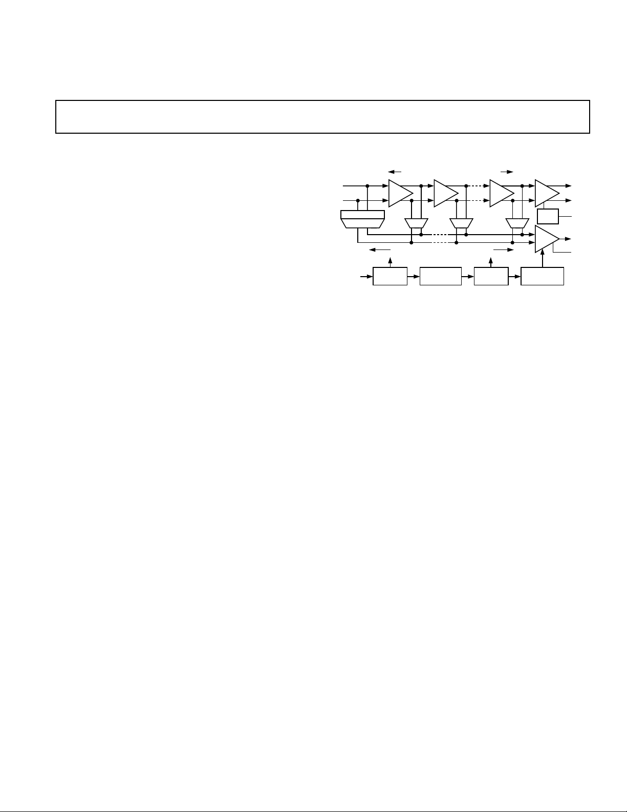
FUNCTIONAL BLOCK DIAGRAM
SIX STAGES TOTAL GAIN 72dB TYP GAIN 18dB
INHI
INLO
LADR ATTEN
ENBL
12dB
TEN DETECTORS SPACED 12dB
GAIN
BIAS
DET DET4 3 DET
BAND-GAP
REFERENCE
12dB
12dB LIM
DET
SLOPE
BIAS
BIAS
CTRL
I–V
INTERCEPT
TEMP COMP
LMHI
LMLO
LMDR
VLOG
FLTR
PRODUCT DESCRIPTION
The AD8306 is a complete IF limiting amplifier, providing both
an accurate logarithmic (decibel) measure of the input signal
(the RSSI function) over a dynamic range of 100 dB, and a
programmable limiter output, useful from 5 MHz to 400 MHz.
It is easy to use, requiring few external components. A single
supply voltage of +2.7 V to +6.5 V at 16 mA is needed, corresponding to a power consumption of under 50 mW at 3 V, plus
the limiter bias current, determined by the application and typi-
cally 2 mA, providing a limiter gain of 90 dB when using 200 Ω
loads. A CMOS-compatible control interface can enable the
AD8306 within about 500 ns and disable it to a standby current
of under 1 µA.
The six cascaded amplifier/limiter cells in the main path have a
small signal gain of 12.04 dB (×4), with a –3 dB bandwidth of
850 MHz, providing a total gain of 72 dB. The programmable
output stage provides a further 18 dB of gain. The input is fully
differential and presents a moderately high impedance (1 kΩ in
parallel with 2.5 pF). The input-referred noise-spectral-density,
when driven from a terminated 50 Ω, source is 1.28 nV/√Hz,
equivalent to a noise figure of 3 dB. The sensitivity of the
AD8306 can be raised by using an input matching network.
Each of the main gain cells includes a full-wave detector. An
additional four detectors, driven by a broadband attenuator, are
used to extend the top end of the dynamic range by over 48 dB.
The overall dynamic range for this combination extends from
–91 dBV (–78 dBm at the 50 Ω level) to a maximum permissible
value of +9 dBV, using a balanced drive of antiphase inputs each of
2 V in amplitude, which would correspond to a sine wave power
of +22 dBm if the differential input were terminated in 50 Ω.
Through laser trimming, the slope of the RSSI output is closely
controlled to 20 mV/dB, while the intercept is set to –108 dBV
(–95 dBm re 50 Ω). These scaling parameters are determined
by a band-gap voltage reference and are substantially independent of temperature and supply. The logarithmic law conform-
ance is typically within ±0.4 dB over the central 80 dB of this
range at any frequency between 10 MHz and 200 MHz, and is
degraded only slightly at 400 MHz.
The RSSI response time is nominally 73 ns (10%–90%). The
averaging time may be increased without limit by the addition of
an external capacitor. The full output of 2.34 V at the maximum
input of +9 dBV can drive any resistive load down to 50 Ω and
this interface remains stable with any value of capacitance on
the output.
The AD8306 is fabricated on an advanced complementary
bipolar process using silicon-on-insulator isolation techniques
and is available in the industrial temperature range of –40°C to
+85°C, in a 16-lead narrow body SO package. The AD8306 is
also available for the full military temperature range of –55°C to
+125°C, in a 16-lead side-brazed ceramic DIP.
REV. A
Information furnished by Analog Devices is believed to be accurate and
reliable. However, no responsibility is assumed by Analog Devices for its
use, nor for any infringements of patents or other rights of third parties
which may result from its use. No license is granted by implication or
otherwise under any patent or patent rights of Analog Devices.
One Technology Way, P.O. Box 9106, Norwood, MA 02062-9106, U.S.A.
Tel: 781/329-4700 World Wide Web Site: http://www.analog.com
Fax: 781/326-8703 © Analog Devices, Inc., 1999

AD8306–SPECIFICATIONS
Parameter Conditions Min
INPUT STAGE (Inputs INHI, INLO)
Maximum Input
2
Differential Drive, p-p ±3.5 ±4V
(VS = +5 V, TA = +25ⴗC, f = 10 MHz, unless otherwise noted)
1
Typ Max1Units
+9 dBV
Equivalent Power in 50 Ω Terminated in 52.3 Ω储R
IN
+22 dBm
Noise Floor Terminated 50 Ω Source 1.28 nV/√Hz
Equivalent Power in 50 Ω 400 MHz Bandwidth –78 dBm
Input Resistance From INHI to INLO 800 1000 1200 Ω
Input Capacitance From INHI to INLO 2.5 pF
DC Bias Voltage Either Input 1.725 V
LIMITING AMPLIFIER (Outputs LMHI, LMLO)
Usable Frequency Range 5 400 MHz
At Limiter Output R
LOAD
= R
= 50 Ω, to –10 dB Point 585 MHz
LIM
Phase Variation at 100 MHz Over Input Range –73 dBV to –3 dBV ±2 Degrees
Limiter Output Current Nominally 400 mV/R
Versus Temperature –40°C ≤ T
Input Range
3
≤ +85°C –0.008 %/°C
A
LIM
0110mA
–78 +9 dBV
Maximum Output Voltage At Either LMHI or LMLO, wrt VPS2 1 1.25 V
Rise/Fall Time (10%–90%) R
= 50 Ω, 40 Ω ≤ R
LOAD
≤ 400 Ω 0.6 ns
LIM
LOGARITHMIC AMPLIFIER (Output VLOG)
±3 dB Error Dynamic Range From Noise Floor to Maximum Input 100 dB
Transfer Slope
4
f = 10 MHz 19.5 20 20.5 mV/dB
f = 100 MHz 19.6 mV/dB
Over Temperature –40°C < T
Intercept (Log Offset)
4
f = 10 MHz –109.5 –108 –106.5 dBV
< +85°C 19.3 20 20.7 mV/dB
A
f = 100 MHz –108.4 dBV
Over Temperature –40°C ≤ T
≤ +85°C –111 –108 –105 dBV
A
Temperature Sensitivity –0.009 dB/°C
Linearity Error (Ripple) Input from –80 dBV to +0 dBV ±0.4 dB
Output Voltage Input = –91 dBV, V
Input = +9 dBV, V
Input = –3 dBV, V
Minimum Load Resistance, R
L
= +5 V, +2.7 V 0.34 V
S
= +5 V 2.34 2.75 V
S
= +3 V 2.10 V
S
40 50 Ω
Maximum Sink Current To Ground 0.75 1.0 1.25 mA
Output Resistance 0.3 Ω
Small-Signal Bandwidth 3.5 MHz
Output Settling Time to 2% Large Scale Input, +3 dBV, R
Rise/Fall Time (10%–90%) Large Scale Input, +3 dBV, R
≥␣ 50 Ω, CL ≤␣ 100 pF 120 220 ns
L
≥␣ 50 Ω, CL ≤␣ 100 pF 73 100 ns
L
POWER INTERFACES
Supply Voltage, V
S
2.7 5 6.5 V
Quiescent Current Zero-Signal, LMDR Open 13 16 20 mA
Over Temperature –40°C < T
Disable Current –40°C < T
Additional Bias for Limiter R
LIM
Logic Level to Enable Power HI Condition, –40°C < T
Input Current when HI 3 V at ENBL, –40°C < T
< +85°C 111623mA
A
< +85°C 0.01 4 µA
A
= 400 Ω (See Text) 2.0 2.25 mA
< +85°C 2.7 V
A
< +85°C4060µA
A
V
S
Logic Level to Disable Power LO Condition, –40°C < TA < +85°C –0.5 1 V
TRANSISTOR COUNT # of Transistors 207 207
NOTES
1
Minimum and maximum specified limits on parameters that are guaranteed but not tested are six sigma values.
2
The input level is specified in “dBV” since logarithmic amplifiers respond strictly to voltage, not power. 0 dBV corresponds to a sinusoidal single-frequency input of
1 V rms. A power level of 0 dBm (1 mW) in a 50 Ω termination corresponds to an input of 0.2236 V rms. Hence, in the special case of 50 Ω termination, dBV values
can be converted into dBm by adding a fixed offset of +13 to the dBV rms value.
3
Due to the extremely high Gain Bandwidth Product of the AD8306, the output of either LMHI or LMLO will be unstable for levels below –78 dBV (–65 dBm, re 50 Ω).
4
Standard deviation remains essentially constant over frequency. See Figures 13, 14, 16 and 17.
Specifications subject to change without notice.
–2–
REV. A
AD8306
WARNING!
ESD SENSITIVE DEVICE
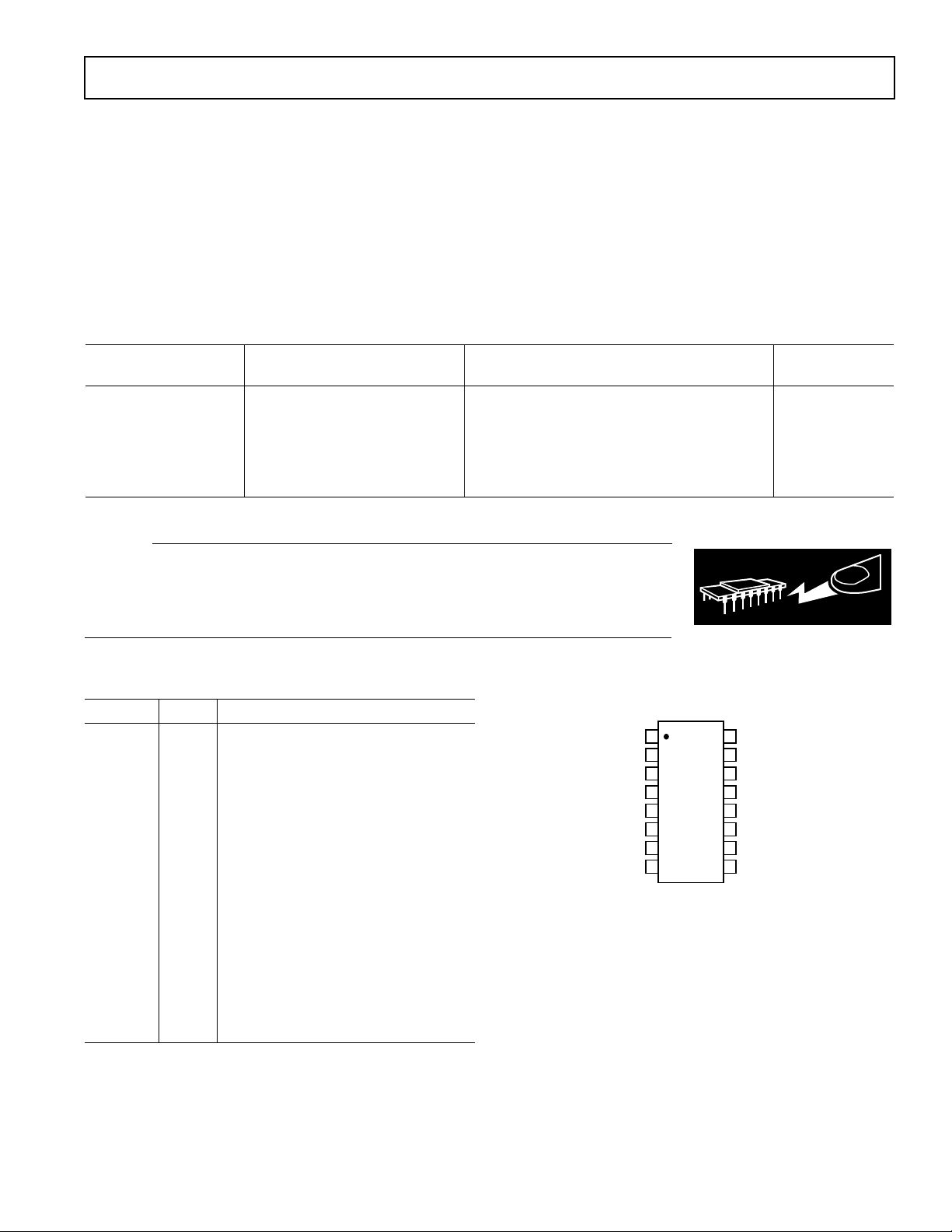
TOP VIEW
(Not to Scale)
16
15
14
13
12
11
10
9
1
2
3
4
5
6
7
8
COM2
VLOG
AD8306
VPS1
PADL
INHI
INLO
PADL
COM1
ENBL
VPS2
PADL
LMHI
LMLO
PADL
FLTR
LMDR
ABSOLUTE MAXIMUM RATINGS*
Supply Voltage VS . . . . . . . . . . . . . . . . . . . . . . . . . . . . . . 7.5 V
Input Level, Differential (re 50 Ω) . . . . . . . . . . . . . . . +26 dBm
Input Level, Single-Ended (re 50 Ω) . . . . . . . . . . . . . +20 dBm
Internal Power Dissipation . . . . . . . . . . . . . . . . . . . . . 800 mW
. . . . . . . . . . . . . . . . . . . . . . . . . . . . . . . . . . . . . . . 125°C/W
θ
JA
θ
. . . . . . . . . . . . . . . . . . . . . . . . . . . . . . . . . . . . . . . . 25°C/W
JC
Maximum Junction Temperature . . . . . . . . . . . . . . . . +125°C
Operating Temperature Range . . . . . . . . . . . . –40°C to +85°C
Storage Temperature Range
–65°C to +150°C
Lead Temperature Range (Soldering 60 sec)
+300°C
*Stresses above those listed under Absolute Maximum Ratings may cause perma-
nent damage to the device. This is a stress rating only; functional operation of the
device at these or any other conditions above those indicated in the operational
section of this specification is not implied. Exposure to absolute maximum rating
conditions for extended periods may effect device reliability.
ORDERING GUIDE
Temperature Package Package
Model Range Description Options
AD8306AR –40°C to +85°C 16-Lead Narrow Body SO SO-16
AD8306AR-REEL –40°C to +85°C 13" Tape and Reel SO-16
AD8306AR-REEL7 –40°C to +85°C 7" Tape and Reel SO-16
AD8306ACHIPS –40°C to +85°CDie
5962-9864601QEA –55°C to +125°C 16-Lead Side-Brazed Ceramic DIP D-16
AD8306-EVAL Evaluation Board
CAUTION
ESD (electrostatic discharge) sensitive device. Electrostatic charges as high as 4000 V readily
accumulate on the human body and test equipment and can discharge without detection.
Although the AD8306 features proprietary ESD protection circuitry, permanent damage may
occur on devices subjected to high energy electrostatic discharges. Therefore, proper ESD
precautions are recommended to avoid performance degradation or loss of functionality.
PIN FUNCTION DESCRIPTIONS
Pin Name Function
1 COM2 Special Common Pin for RSSI Output.
2 VPS1 Supply Pin for First Five Amplifier Stages
and the Main Biasing System.
3, 6, 11, 14 PADL Four Tie-Downs to the Paddle on
which the IC Is Mounted; Grounded.
4 INHI Signal Input, HI or Plus Polarity.
5 INLO Signal Input, LO or Minus Polarity.
7 COM1 Main Common Connection.
8 ENBL Chip Enable; Active When HI.
9 LMDR Limiter Drive Programming Pin.
10 FLTR RSSI Bandwidth-Reduction Pin.
12 LMLO Limiter Output, LO or Minus Polarity.
13 LMHI Limiter Output, HI or Plus Polarity.
15 VPS2 Supply Pin for Sixth Gain Stage, Limiter
and RSSI Output Stage Load Current.
16 VLOG Logarithmic (RSSI) Output.
REV. A
PIN CONFIGURATION
–3–
AD8306
100
–Typical Performance Characteristics
10
0.1
0.01
0.001
SUPPLY CURRENT – mA
0.0001
0.00001
1
0.5
TA = +258C
TA = +858C
0.7 0.9 1.1 1.3 1.5 1.7 1.9 2.1 2.3 2.5
ENABLE VOLTAGE – V
TA = –408C
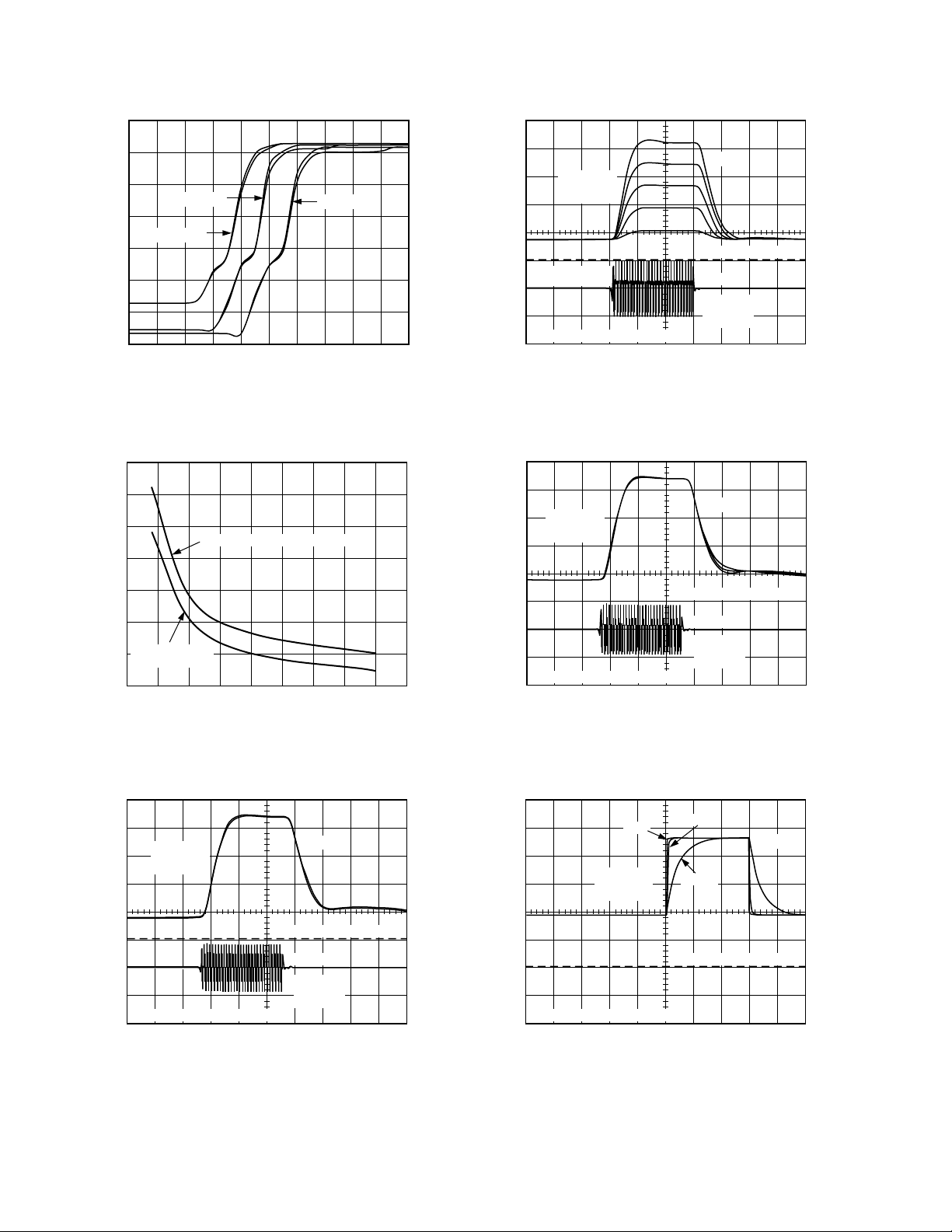
Figure 1. Supply Current vs. Enable Voltage @
= –40°C, +25°C and +85°C
T
A
14
12
10
8
6
4
SUPPLY CURRENT – mA
LIMITER OUTPUT
2
CURRENT
0
50 100 150 200 250 300 350 400 450
0
ADDITIONAL SUPPLY CURRENT
R
– V
LIM
Figure 2. Additional Supply Current and Limiter Output
Current vs. R
LIM
VLOG
500mV PER
VERTICAL
DIVISION
INPUT LEVEL
SHOWN IS –3dBV
100ns PER HORIZONTAL DIVISION
GROUND REFERENCE
INPUT
1V PER
VERTICAL
DIVISION
Figure 4. RSSI Pulse Response for Inputs Stepped from
Zero to –83 dBV, –63 dBV, –43 dBV, –23 dBV, –3 dBV
500mV PER
VERTICAL
DIVISION
VLOG
GROUND REFERENCE
INPUT
2V PER
VERTICAL
100ns PER HORIZONTAL DIVISION
DIVISION
Figure 5. Large Signal RSSI Pulse Response with RL = 100
and CL = 33 pF, 100 pF and 330 pF (Overlapping Curves)
Ω
500mV PER
VERTICAL
DIVISION
VLOG
GROUND REFERENCE
INPUT
2V PER
VERTICAL
100ns PER HORIZONTAL DIVISION
DIVISION
Figure 3. Large Signal RSSI Pulse Response with
= 100 pF and RL = 50Ω and 75Ω (Curves Overlap)
C
L
27pF
200mV PER
VERTICAL
DIVISION
270pF
VLOG
3300pF
GROUND REFERENCE
100ms PER HORIZONTAL DIVISION
Figure 6. Small Signal AC Response of RSSI Output with
External Filter Capacitance of 27 pF, 270 pF and 3300 pF
–4–
REV. A
AD8306
2.5
2
1.5
1
RSSI OUTPUT – V
0.5
TA = +858C
TA = +258C
0
–120
TA = –408C
–100 –80 –60 –40 –20 0 20
(–87dBm) (+13dBm)
INPUT LEVEL – dBV
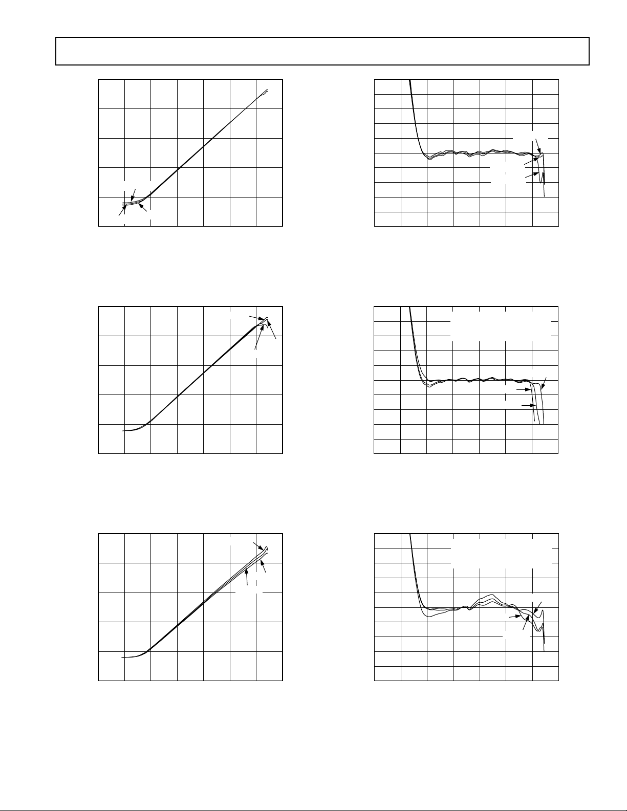
Figure 7. RSSI Output vs. Input Level, 100 MHz Sine Input, at T
= –40°C, +25°C and +85°C, Single-Ended Input
A
2.5
2
1.5
1
RSSI OUTPUT – V
0.5
0
–120
–100 –80 –60 –40 –20 0 20
(–87dBm) (+13dBm)
INPUT LEVEL – dBV
100MHz
50MHz
10MHz
Figure 8. RSSI Output vs. Input Level, at TA = +25°C, for
Frequencies of 10 MHz, 50 MHz and 100 MHz
5
4
3
2
1
0
–1
ERROR – dB
–2
–3
–4
–5
–120
–100 –80 –60 –40 –20 0 20
(–87dBm) (+13dBm)
(–87dBm)
INPUT LEVEL – dBV
TA = +858C
TA = +258C
TA = –408C
Figure 10. Log Linearity of RSSI Output vs. Input Level,
100 MHz Sine Input, at T
5
4
3
2
1
0
–1
ERROR – dB
–2
–3
–4
–5
–120
–100 –80 –60 –40 –20 20
–100
(–87dBm)
= –40°C, +25°C, and +85°C
A
DYNAMIC RANGE 61dB 63dB
10MHz 86 93
50MHz 90 97
100MHz 96 100
10MHz
50MHz
0
INPUT LEVEL – dBV
(+13dBm)
100MHz
Figure 11. Log Linearity of RSSI Output vs. Input Level, at
= +25°C, for Frequencies of 10 MHz, 50 MHz and 100 MHz
T
A
2.5
2
1.5
1
RSSI OUTPUT – V
0.5
0
–120
–100 –80 –60 –40 –20 0 20
(–87dBm) (+13dBm)
INPUT LEVEL – dBV
200MHz
400MHz
300MHz
Figure 9. RSSI Output vs. Input Level, at TA = +25°C, for
Frequencies of 200 MHz, 300 MHz and 400 MHz
REV. A
5
4
3
2
1
0
–1
ERROR – dB
–2
–3
–4
–5
–120
–100 –80 –60 –40 –20 20
–100
(–87dBm)
DYNAMIC RANGE 61dB 63dB
200MHz 96 100
300MHz 90 100
400MHz 85 100
400MHz
300MHz
INPUT LEVEL – dBV
200MHz
0
(+13dBm)
Figure 12. Log Linearity of RSSI Output vs. Input Level,
= +25°C, for Frequencies of 200 MHz, 300 MHz and
at T
A
400 MHz
–5–
 Loading...